Abstract
In this study, plasma display panels with three different cell volumes were prepared by changing the spaces between the vertical barrier ribs into two and three times the reference structure. The discharge gap and area of the segmented ITO electrode were the same for the three cases, and Ne–20%Xe gas was used. The luminance and luminance efficiency were measured using applied voltage variations. The time evolution and intensity distribution of the infrared, which are related to the vacuum ultraviolet, were observed via intensified, charged, coupled device, and the visible-light intensity profiles were observed using PR-900 to analyze the discharge phenomena in the discharge cell.
1. Introduction
Many studies have been conducted with the aim of increasing the luminance efficiency of a plasma display panel (PDP) through the optimization of the discharge mode, by using a higher Xe gas content Citation1, changing the position of the bus electrode Citation2, using a new-type sustaining electrode Citation3, using a counter-type electrode configuration Citation4, separating the bus electrodes from the indium tin oxide (ITO) electrode lines Citation5, adapting an auxiliary electrode Citation6, or using a narrower ITO structure Citation7. All these approaches are based on gas-discharge physics, in which the incremental number of electron creation and excitation is important for the luminance efficiency. Boeuf and co-workers Citation8 analyzed the discharge characteristics of a plasma display cell via macrocell experiments and 3D simulations. They observed the space and time evolution of the infrared Xe light emission for the 5-cm coplanar gap length and concluded that the ratio of the infrared-to-visible emission is a good indicator of the discharge efficiency in xenon excitation and, therefore, in UV photon production. In the same sense, the luminance efficiency is related to the volume of the cell size internal to the PDP because the number of and distance between the excited species are changed with the variation of the discharge cell volume.
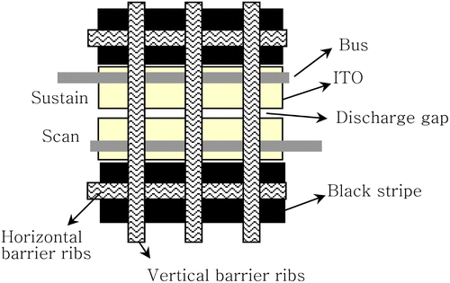
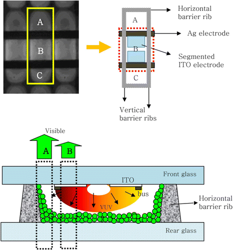
shows an overlapped image of the front and rear substrates of a PDP, in which it is shown that the discharge cell volume is determined by the horizontal and vertical barrier ribs. The discharge cell volume was observed to have two different effects. First, the barrier ribs that surround the discharge cell volume confine the movement and the collisions of the gas molecules. Second, the barrier ribs are electrically dielectric, so some of the electrical power is spent in the form of capacitive loss in proportion to their dielectric constants. For these reasons, the electrode designs concerned with the barrier ribs may also influence the luminance efficiency of the PDP cell. Therefore, it is understood that the optimum design of the distance between the barrier ribs is important to gain high luminance efficiency.
Figure 1. The overlapped image of the front and rear panel structures for a cell in a PDP.
In this study, the luminance and discharge characteristics of discharge cells with different cell volumes were observed by changing the distance between the barrier ribs. A segmented ITO structure and a matrix-type barrier rib structure were used as it is common to use them to enhance the luminosity.
2. Experimental procedure
Three-inch test panels were manufactured with a cell size of m2 following the general specification of a 50″ XGA
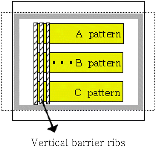
PDP. ITO-coated 2.8-mm-thick PD200 (Asahi Glass Co.) glass substrates were used for the front substrates. The ITO electrode pattern was manufactured via photolithography, using a dry-film resist film. The bus electrode pattern was also manufactured via photolithography, in which a photosensitive Ag-based paste was printed, dried, exposed, developed, and fired. The black matrix was formed via photolithography with a photosensitive black-colored paste. The design of the ITO electrodes, bus electrodes, and black matrix were modified to obtain a higher bright-room contrast ratio and a higher luminance efficiency. To decrease the experimental errors, the conventional and new electrode patterns were placed together on the same panel, as shown in . A 30-μm-thick transparent dielectric layer was formed on the ITO and bus electrodes and was then coated with a 6000-Å-thick MgO layer via the electron beam evaporation method.
Figure 2. The basic configuration of the ITO electrode patterns for the comparison of the luminous efficiency in this study.
For the rear substrates, 2.8-mm-thick PD200 glass substrates were also used. The address electrode pattern was manufactured using the same method as that which was used for the bus. The barrier ribs were manufactured via the chemical etching method, and green phosphors were printed into the cell volumes. The front and rear substrates were assembled using sealing frits, followed by evacuation at 350 °C. Finally, the inner cell spaces were filled with Ne–20%Xe gas mixtures under 400 Torr. The discharge characteristics and luminance of the panel were measured under a 25 kHz, 25% continuous duty-sustaining condition.
Luminance and luminance efficacy are defined as
The infrared (IR) intensity profiles of the discharge cell were obtained using a high-speed, intensified, charged, coupled device (ICCD; Princeton Instrument) camera with an applied voltage of 230 V. IR images were taken with an optical band-pass filter centered at 820–830 nm, with a 10-nm bandwidth full-width at half-maximum along with a 10-ns gate width. As it is well known that the 823 and 828 nm IR peaks are related to the intensities of 173- and 147-nm vacuum ultraviolet (VUV), the intensity of the VUV, which is used to excite the phosphors to make a visible light, can be obtained by investigating the IR peaks. The intensity profile of the visible light in a discharge cell was measured using the PR-900 with a photo filter.
shows the several structural factors of the cells, which were composed of the x and y electrodes and the barrier ribs. The discharge started from the region between the two fronts of the segmented ITO electrodes (x and y) as the discharge voltage was at a minimum when the electrode gap had the minimum length. There are two kinds of barrier ribs, the horizontal and vertical barrier ribs, and A and B in are the distances between the electrodes and the horizontal and vertical barrier ribs, respectively. When plasma is generated inside the cell, the numbers of the discharge species, such as the positive ions, electrons, neutral atoms, and excited atoms, increase at a high rate, and the discharge species collide with the surrounding barrier ribs. Therefore, the distance between the electrodes and the barrier ribs influences the electrical characteristics of the cell, which was mainly investigated in this study.
Figure 3. Explanation of the several structural factors of the cells which are composed of the x and y electrodes and the barrier ribs.
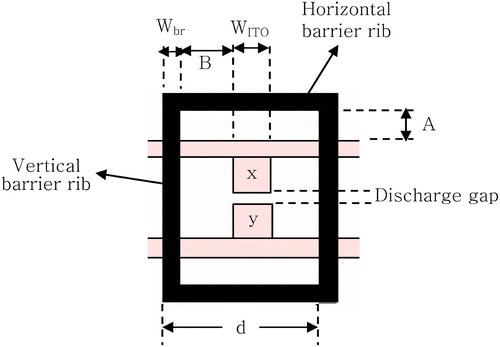
In this study, A was kept constant and B was varied to investigate the effects of the cell volume on the luminance characteristics, which translates to
Table 1. Comparison of the values of the structural elements for the three kinds of cell structures.
3. Results and discussion
3.1. Luminance characteristics of the test panels with different cell volumes
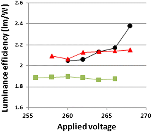
shows the luminance values for the three different cell structures d=270, 540, and 810 μm, which were measured according to the variations of the applied voltage. It can be seen from that the luminance values increase with an increase in the applied voltage, as is well known. Comparing the three cases, the d=270, 540, and 810 μm, the 270 and 540 μm cases are similar, but they show about 20% higher luminance values than that seen in the 810-μm case. shows the power consumption of the PDP panel, which was measured according to the variations of the applied voltage. It can be seen that the 270- and 540-μm cases show higher power consumption values than the 810-μm case, similar to the luminance value relationship in . As a result, the luminance efficiency values were calculated using EquationEquation (1), as shown in . It can be seen that the 270- and 540-μm cases show higher luminance efficiency values (about 10% higher), ranging within 2.0 and 2.2 lm/W, compared to the 810-μm case, with about 1.9 lm/W luminance efficiency values under the same voltage measurement conditions. This means that not only the luminance, but also the luminance efficiency value of the 810-μm case is lower than those of the 270- and 540-μm cases. To investigate these results, optical analyses, including those of the IR and visible-light intensity profiles, were carried out.
Figure 4. The luminance values with the applied voltage for the three different cell structures, d=270, 540, and 810 μm.
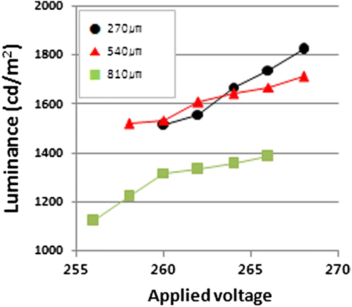
Figure 5. The power consumption values with the applied voltage for the different cell structures, d=270, 540, and 810 μm.
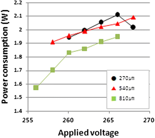
Figure 6. The luminous efficiency values with the applied voltage for the different cell structures, d=270, 540, and 810 μm.
3.2. Investigation of the IR and visible-light distribution in the discharge cells
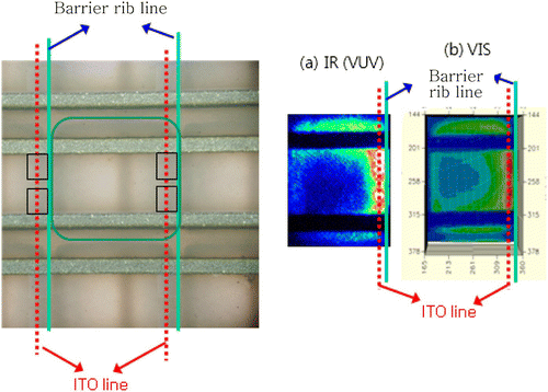
shows the IR intensity profiles of the discharge cell investigated using the ICCD images during the discharge processes for the different cell structures (d=270, 540, and 810 μm). shows the time evolution of the IR intensity profiles, in which each photograph shows the intensity observed for 20 ns. It is shown that the moments of the plasma evolution are similar for all the three cases. The plasma continues for a similar period for the three cases. is the summation of the IR intensity profiles of the 50 photographs taken during the total measurement time. The comparison of the intensity profiles with the original electrode designs, which is shown in for each case, will reveal that the IR wave comes from the segmented ITO electrode area. Therefore, the amount of the IR wave depends on the segmented ITO electrode area.
Figure 7. The IR intensity profiles of the discharge cell investigated by ICCD images during the discharge processes for the different cell structures, d=270, 540, and 810 μm. (a) Time evolution of the IR intensity profiles (total 50 photographs for each case). (b) Summation of the IR intensity profiles during the total measuring time. (c) Schematic drawings of the original electrode designs for each case.
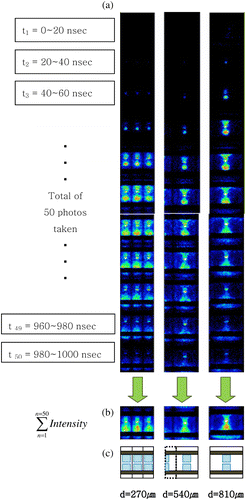
The comparison of the d=270- and 810-μm cases in will reveal that the IR emission area of the d=270-μm case is about three times that of the d=810-μm case because the number of the segmented ITO electrodes of the d=270-μm case is three times greater than that of the d=810-μm case. It is shown that the IR emission for the d=810-μm case is observed only on the segmented ITO area even though the size of the cell itself is three times larger than that of the d=270-μm case. By contrast, shows the 2D luminance profiles for the visible light investigated using PR-900 within the discharge cell for the different cell structures d=270, 540, and 810 μm. It is interesting that the visible lights are distributed all over the cell even though the IR emission is concentrated only on the segmented ITO area for d=810 μm in . The high-luminance-intensity area is expressed with the red color in the figure, and it can be seen that the distribution profiles of the luminance intensity are different for the three cases. In the case of d=810 μm, the high-luminance-intensity area is found near the sidewall, where no IR emission was found in . These results will be explained in connection to the cell structures in .
Figure 8. The 2D luminance profiles investigated by PR-900 during the discharge process for the different cell structures, d=270, 540, and 810 μm.
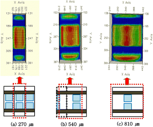
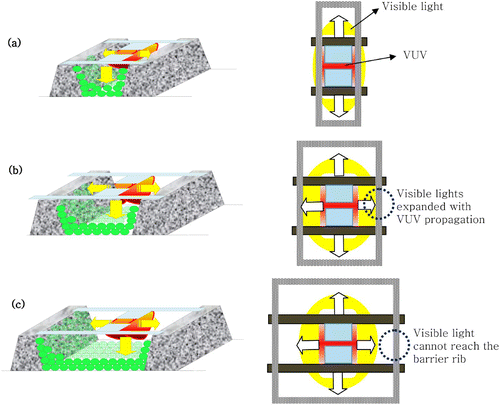
Figure 9. A schematic drawing of the inside of the discharge cell.
First, for the d=270-μm case in , the sidewall of the cell shows the highest luminance intensity. This can be explained using the schematic drawing of the inside of the cell in . There are two kinds of barrier ribs: the horizontal and the vertical. As the VUV emissions are formed mainly on the segmented ITO electrode area, as was mentioned earlier, area B in the figure is full of VUV, which collides with the phosphors coated onto the barrier ribs. As shown in , the VUV, which was formed by the electric field, reaches the bottom of the barrier rib, spreads out on the surface of the phosphor, and attains uniform distribution in visible light. The cross-section of the barrier rib has a slight slope on the sidewall due to the characteristics of the lithography process. Thus, the amount of phosphor in area A is greater than that in area B, as shown in . It is believed that this explains why the sidewalls of the cell show the highest luminance intensity for the d=270-μm case in .
Second, for the d=540-μm case in , the red-colored regions with the highest luminance intensity are distributed all over the cell area, including the segmented ITO and sidewall areas. It is known from that the VUV emission intensities exist mainly on the segmented ITO area and spread out into the whole cell volume. They collide with several kinds of species, which include positive ions, electrons, and neutral atoms, but they keep their energy until they reach the sidewall of the barrier rib. Therefore, strong visible light is observed over the entire cell area.
In this study, an ICCD camera with an 823-nm IR filter was used to observe the VUV emission, and PR-900 was used to observe the visible-light emission. PR-900 that was used in this study adopted a photo filter, which passed the visible wavelength. Therefore, in this study, the data that were obtained from PR-900 included not only the visible emission from the phosphors (only green phosphors were used in this study), but also the orange emission from the Ne* atoms. It is true that IR emissions can indicate the population of Xe* excited atoms. VUV, especially 147 nm, will frequently experience absorption by Xe atoms in the ground state and will be regenerated. With the repetition of self-absorption, VUV will propagate to the phosphor layer, but the visible emission of R, G, and B from the phosphor layers can still be attained. The VUV propagation along the phosphor may be investigated by observing the IR emission. In this study, however, the IR emission was seen only in the vicinity of the ITO electrode, as shown in the ICCD pictures in , which means that the behavior of the VUV propagation that started from the ITO electrode is not represented by the 823-nm IR emission. Two possibilities are seen as reasons for this. First, during the collision and absorption, the wavelength is changed; as such, the modified VUV emission can no longer be detected by the 823-nm filter. Second, after the collision with the phosphor atoms, the VUV emission is weakened and thus cannot be well detected by the ICCD camera due to the weak intensity.
Third, for the d=810-μm case in , the red-colored regions with the highest luminance intensity are distributed only in the middle of the cell, coinciding with the segmented ITO area. In contrast with and , no red-colored region can be found outside the sidewall area in . In this case, it is shown that the VUV emitted on the segmented ITO area spreads out over the whole cell volume, colliding with several kinds of species and thus losing their energy through collisions, absorptions, etc. during the long trip before reaching the barrier rib walls. Therefore, it is assumed that there are few ultraviolet waves near the sidewalls of the barrier ribs, for which reason high-luminance-intensity lights are not observed there. is a schematic drawing that shows the distribution of the IR (VUV) and VIS emissions in a PDP cell in which segmented ITO electrodes are aligned near the sidewall. It is shown that the distribution of the IR emission cannot reach the opposite sidewall, and the visible light is not observed either in that region. supports this assumption in the sense that the propagation of the VUV is restricted within some distance in accordance with the result shown in .
Figure 10. A schematic drawing which shows the distribution of the IR (VUV) and VIS in a PDP cell when the segmented ITO is aligned near the sidewall.
shows the schematic drawings that explain the formation of the ultraviolet and visible light, and their propagation in a plasma display cell. In the plasma display, the 823- and 828-nm IR emission peaks from Xe are closely related to the VUV, with wavelengths of 173 and 147 nm and excitation energies of 8.32 eV (Xe2*) and 8.44 eV (Xe*), respectively. Thus, the intensity of the IR emission from Xe indicates the amount of VUV that is formed near the segmented ITO electrode, as seen in . This can be explained by the fact that electrons become extinct through recombination with positive ions, so they cannot spread out inside the discharge cell. The ultraviolet rays spread out by colliding with the gas atoms in the cell volume.
Figure 11. The schematic drawing which shows the propagation of the ultraviolet and visible lights in a cell of plasma display. (a) d=270 μm; (b) d=540 μm; (c) d=810 μm.
In the case of fluorescent lamps, as the inside of the lamp is filled with low-pressure (1–10 mTorr) discharge gases, the electrons can travel over a long distance. Therefore, much of the glow discharge volume is occupied by a positive column, in which high-energy electrons have a small cross-section for the elastic collision due to the short collision time. That is why visible light spreads uniformly in a fluorescent lamp, and why high luminance efficiency can be obtained. In the case of PDP, however, the distance between the electrodes is very short (about 100 μm), and the gas pressure is very high (400–500 Torr), so the ultraviolet rays lose their energy through their many collisions with the discharge gases.
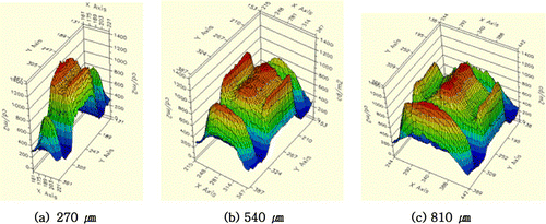
shows a 3D presentation of the luminance profiles in , in which it can be seen that the maximum peak luminance is 1200, 1000, and 800 cd/m2 for d=270, 540, and 810 μm, respectively. This means that the peak luminance decreases as the cell volume increases in this experiment. The differences in several characteristics, including the luminance, power consumption, and luminance efficiency, in and 12 can be explained using the conceptual drawings in . In the case of d=270 μm in , the cell volume is filled with ultraviolet rays and visible light. As such, the luminance is high, but there is a large amount of capacitive loss through the sidewall of the barrier ribs. In the case of d=540 μm in , the ultraviolet rays spread out to some degree, which makes the visible light fill the cell volume, as shown in . The luminance is not as high as in the case of d=270 μm, and there is less capacitive loss through the sidewall of the barrier ribs. It is believed that this explains why the luminance efficiency was observed to be similar to that in the case of d=270 μm, as shown in . On the other hand, in the case of d=810 μm in , the ultraviolet rays, and thus the visible light, occupy a small area, not reaching the sidewall of the barrier ribs. The luminance is very low in this case, that is why the luminance efficiency was observed to be lower in the case of d=810 μm in .
Figure 12. The 3D luminance profiles investigated by PR-900 during the discharge process for the different cell structures, d=270, 540, and 810 μm.
4. Conclusion
In this study, PDPs with three different cell volumes were compared with the variation of the spaces between the adjacent vertical barrier ribs (d=270, 540, and 810 μm). The luminance efficiency values were similar in the cases of d=270 and 540 μm, but a lower value was observed in the case of d=810 μm. In the ICCD investigation, VUV emission was observed only in the vicinity of the ITO electrode. As such, there were big differences in the VUV emission area among the three different cell volumes (d=270, 540, and 810 μm) due to the differences in the number of their ITO segments. On the other hand, the observation of visible-light emission using PR-900 showed that the distribution of the visible-light emission was similar for d=270 and 540 μm. It is assumed that this is because the VUV generated in the vicinity of the ITO electrode propagates all over the cell volume through the phosphor layer. By contrast, the visible-light emission was weaker in the d=810-μm case compared to the d=270- and 540-μm cases. The energy of the VUV cannot reach the sidewall of the barrier ribs due to the large distance in the case of d=810 μm, which leads to weak visible-light emission and lower luminance efficiency.
Acknowledgements
This work was supported by the IT R&D program of MKE/KEIT [2009-S-009-01, “Development of an Eco-friendly 50” Quadro Full-HD PDP Technology”]
References
- Chung , W. J. , Shin , B. J. , Kim , T. J. , Bae , H. S. , Seo , J. H. and Whang , K. W. 2003 . IEEE Trans. Plasma Sci. , 31 ( 5 ) : 1038
- Kang , J. 2006 . IEEE Trans. Plasma Sci. , 34 ( 2 ) : 371
- Park , C. H. , Lee , S. H. , Kim , D. H. , Kim , Y. K. and Shin , J. H. 2001 . IEEE Trans. Electron Dev. , 48 ( 10 ) : 2255
- Hur , M. , Kim , J. R. , Yi , J. D. , Cho , Y. H. , Song , S. B. , Park , J. Y. and Lee , H. Y. 2006 . J. Appl. Phys. , 99 : 113301
- Moon , C. H. and Kim , K. N. 2008 . Jpn. J. Appl. Phys. , 47 ( 4 ) : 2259
- Choi , K. C. , Shin , N. H. , Song , S. C. , Lee , J. H. and Park , S. D. 2007 . IEEE Trans. Electron Dev. , 54 ( 2 ) : 210
- Akiyama , T. , Yamada , T. , Kitagawa , M. and Shinoda , T. 2009 . J. SID , 17 ( 2 ) : 121
- Ouyang , J. , Callegari , Th. , Caillier , B. and Boeuf , J. P. 2003 . IEEE Trans. Plasma Sci. , 31 ( 3 ) : 422