Abstract
A single-clock-driven shift register and a two-stage buffer are proposed, using p-type, low-temperature polycrystalline silicon thin-film transistors. To eliminate the clock skew problems and to reduce the burden of the interface, only one clock signal was adopted to the shift register circuit, without additional reference voltages. A two-stage, p-type buffer was proposed to drive the gate line load and shows a full-swing output without threshold voltage loss. The shift register and buffer were designed for the 3.31″ WVGA (800×480) LCD panel, and the fabricated circuits were verified via simulations and measurements.
1. Introduction
There are many candidates for the backplanes of flat-panel displays, such as hydrogenated amorphous silicon thin-film transistors (a-Si:H TFTs), polycrystalline silicon (poly-Si) TFTs, organic TFTs Citation1, and oxide-based TFTs Citation2. Among the various backplane transistors, low-temperature polycrystalline silicon (LTPS) TFTs are the most suitable for high-resolution mobile displays due to their superior mobility, relative low-temperature process, and possibilities of integrating a gate driver, a DC–DC converter, and even a source driver into the display panel using complementary metal-oxide-semiconductor (CMOS) LTPS TFTs or only p-type LTPS TFTs.Footnote
The CMOS LTPS TFT process, however, has the drawback of increased process cost due to its increased process steps, such as laser crystallization of silicon and n- or p-type ion doping. By employing only the p-type LTPS TFT process, the masks for n-LDD (lightly doped drain) doping and n+ source/drain doping for n-type TFTs can be eliminated, as opposed to the CMOS process. With the process steps reduced, the process time will become much shorter, and the process yield can be expected to increase, so that the fabrication cost can be reduced further.
Although they have cost competitiveness over CMOS LTPS TFTs, p-type circuits have disadvantages, such as difficulty in making high-performance circuits, increased power consumption and limitation of output voltage range, compared to the CMOS-type circuits. In spite of the aforementioned restrictions, several driving circuits using only p-type LTPS TFTs were reported Citation3–6, but the previously reported shift registers adopted two Citation4 Citation5 or four phase clock signals Citation3, which can induce a clock skew problem. A shift register that adopted only one clock signal was reported by Jung et al. Citation6, but they used an additional low reference voltage, −40 V, to obtain an output voltage swing of 0 to −20 V. This means that a DC–DC converter for producing an additional low reference voltage should be added for the shift register. p-type buffers for the gate driver were rarely reported, and only the transistor size of the output stage of the shift registers or level shifters were increased to drive the gate line load.
In this paper, a gate driver composed of a shift register and an output buffer and using p-type LTPS TFTs is proposed. The proposed shift register employed only one clock signal, without additional reference voltages. By employing only one clock signal, clock-skew-induced problems were fundamentally eliminated Citation6, and the burden of the interface can be reduced. The proposed buffer consists of a coarse inverter and a two-stage inverter string, and the buffer shows a full-swing output without threshold voltage loss.
2. Proposed gate driver
The purpose of this work is to design a gate driver for the 3.31″ WVGA () liquid crystal display (LCD) panel using p-type LTPS TFTs. The transfer characteristics and
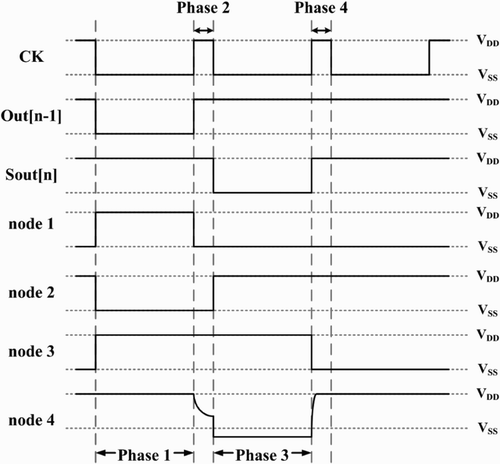
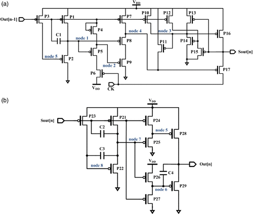
characteristics of the p-type LTPS TFT are shown in and . The threshold voltage and field effect mobility of the TFT were −2.32 V and 53.5 cm/V s, respectively. The proposed gate driver consists of a single-clock-driven shift register and a buffer that does not suffer from output voltage loss. shows the schematic diagram of the proposed shift register, which comprises 17 p-type transistors and employs only one clock signal, without additional reference voltages. The width-to-length (W/L) ratios of the TFTs were 10:7 μm for P3, P6, P7, P10, P11, P12, and P15; 20:7 μm for P1, P4, P5, and P13; 60:7 μm for P8 and P9; 3:9 μm for P2 and P14; and 100:7 μm for P16 and P17. The proposed circuit does not need an additional mask signal and additional circuits to avoid overlapping between the adjacent output signals of the shift register, because gate signals are transferred only when the voltage level of the CK signal is low, as shown in the timing diagram in . In other words, the CK signal includes the mask timing, phases 2 and 4, for the output of the shift register. In the timing diagram in , the timing steps were divided into four steps, from phases 1 to 4, to explain the operation of the shift register. Phase 1 is the time when the input signal comes from the previous stage, and phase 3 is the time when the output signal is transferred to the gate line and input terminal of the next stage. The pull-down transistor, P17, is turned on in phase 2 to prepare to make the output signal low at phase 3. Phase 4 is the time to make the voltage level of the output node high again. In the schematic diagram of the shift register, the transistors from P1 to P3 and from P13 to P15 work as inverters. As the aspect ratio of the pull-up transistor (P1 or P13) is much larger than that of the pull-down transistor (P2 or P14), the output voltage of the inverter, which is high in the case of a low voltage level, is applied to the input terminal. If V
DD is applied to the input, the P1 and P3 transistors are turned off, and the voltage of the output node becomes V
SS through the bootstrapping effect Citation7, with a floating gate node of transistor P2.
Figure 1. (a) Transfer characteristics and (b) I d−V ds characteristics of the p-type LTPS TFT.
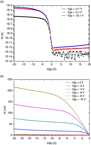
Figure 2. Schematic diagram of the proposed p-type shift register.
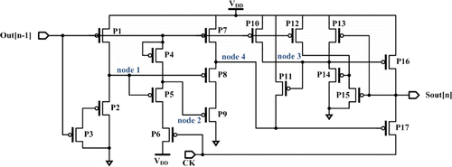
Figure 3. Timing diagram of the proposed p-type shift register.
. Brief comparison of various p-type shift registers
The detailed operations of the proposed shift register will be explained using a timing diagram. In phase 1, because the CK and Out[n−1] signals are low, the voltage levels of nodes 1, 3, and 4 become high, and that of node 2 becomes low. The Sout[n] node is floating and maintains a high voltage because both the pull-up and pull-down transistors are turned off. An inverter consisting of transistors from P13 to P15 does not work because transistor P14 is turned off. In phase 2, the voltage levels of the CK and Out[n−1] signals become high, and those of nodes 1 and 4 become low. The pull-up transistor, P16, is still turned off, but P17 is turned on to deliver a high voltage level of the CK signal to the Sout[n] node. As transistor P17 is turned on, the output voltage level follows the CK signal after phase 2. In phase 3, the CK signal becomes low again, and the voltage of node 4 decreases sufficiently via capacitive coupling with the CK signal. As the voltage level of node 4 is much lower than V SS, the pull-down transistor, P17, transfers V SS to the Sout[n] node without threshold voltage loss. The inverter, which consists of transistors from P13 to P15, makes the voltage level of node 3 high to turn off the pull-up transistor. Thus, a shifted output signal is obtained in phase 3. In phase 4, the CK signal becomes high again, and the voltage level of the Sout[n] node rises to V DD due to the CK signal, because transistor P17 is still turned on at first. As the Sout[n] node is the input of the inverter in the output stage, the voltage level of node 3 becomes low and that of node 4 becomes high. The voltage level of the output node eventually becomes V DD because the pull-up transistor is turned on. After phase 4, the output voltage level remains high because the output stage, which is composed of transistors from P10 to P17, works as a latch. Unless the inverter in the output stage is turned off or is initialized by an In signal, the pull-up transistor, P16, will always be turned on to make the output voltage level high.
compares various p-type shift registers, including the proposed circuit. Although the proposed shift register is more complex than that in the previous work Citation6, the stability of the shift register was improved by reducing the floated time at the gate nodes of the pull-up and pull-down transistors. The proposed circuit also has benefits in terms of the required number of clocks and additional signals. The maximum operation frequency of the proposed circuit is about 2.8 MHz, and the speed of the proposed circuit is enough to be adapted to the gate driver of displays, because the operation frequency of the gate driver for the 240 Hz FHD () TV is about 130 kHz.
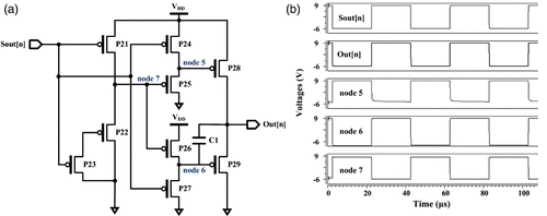
shows the schematic diagram, and the simulation results, of the proposed p-type buffer for use in driving a gate line load with a 15 pF capacitance and a resistance. The proposed buffer consists of a coarse inverter composed of transistors from P21 to P23, and of a two-stage p-type inverter. The W/L ratios of the TFTs were 20:7 μm for P21, 3:9 μm for P22, 10:7 μm for P23, 40:7 μm for P24-P27, and 200:7 μm for P28 and P29. Capacitor C1, which connects the output of the first-stage inverter to that of the second-stage inverter, is used to ensure a full-swing output through the bootstrapping effect Citation7 of node 2, as shown in the simulated waveforms in .
Figure 4. (a) Schematic diagram and (b) simulation results of the proposed p-type buffer.
. Simulation and measurement conditions
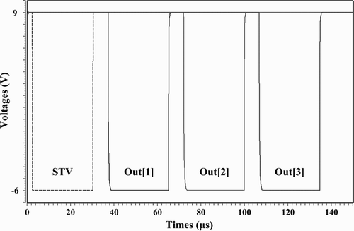
shows the simulation and measurement conditions for the proposed gate driver. The target application was the 3.31″ WVGA () LCD panel, and the frame frequency was 60 Hz. The supply voltage range of the gate driver was from −6 to 9 V, to turn the switching TFTs in pixels on or off. shows the simulation results of the gate driver, which is composed of a single-clock-driven shift register and a buffer for driving the panel's gate line load. The gate driver was operated successfully with only a single clock signal, and the total power consumption of the gate driver was 1.76 mW.
Figure 5. Simulation results of the proposed gate driver.
As the proposed gate driver includes p-type inverters, its schematic diagram can be varied simply by replacing the p-type inverters. For example, to reduce the power consumption of the proposed gate driver, a modified structure of the p-type poly-Si inverter Citation6 can be used to replace the inverters in and (a), as shown in . When the Out[n−1] signal is low, the voltage of node 1 is V
DD and the gate voltage of transistor P5 also becomes V
DD to turn off the pull-down transistor, P2. When the Out[n−1] signal rises to V
DD, the voltage of node 1 becomes much larger than V
DD, and that of node 5 becomes slightly larger than V
DD via capacitive coupling, because capacitor C1 is larger than the parasitic capacitances of node 1. If the voltage difference between nodes 1 and 5 is larger than , the voltage level of node 1 decreases rapidly through transistor P2, which operates in the saturation region. The voltage of node 5 also decreases with capacitive coupling, with the decreasing voltage level of node 1. The lowered voltage level of node 5, which is less than
, ensures that the output of the inverter will become V
SS. Thus, the inverter has a full-swing output and does not suffer from a short-circuit current through the pull-down transistor. The modified gate driver was simulated with the same conditions as those shown in , and the power consumption of the gate driver was 1.13 mW.
Figure 6. Schematic diagrams of (a) the modified shift register and (b) the buffer.
3. Results and discussion
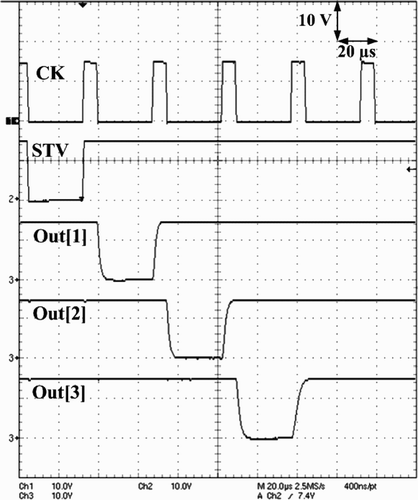
The proposed gate driver test patterns were fabricated on a glass substrate using the p-type LTPS TFT process. shows the micrograph of the 10-channel gate driver, and shows the single-stage gate driver, which consists of the shift register shown in and the output buffer shown in . As the width of the unit gate driver test pattern is 825 μm, the gate driver can be integrated into the panel while consuming a small area to ensure the compact size of the bezel for the mobile display panel. Measurement was conducted for the 10-channel gate driver circuits, using a probe station (SUMMIT 12971B, Cascade Microtech, Beaverton, OR), and the measurement conditions were the same as those in the simulations, as shown in . The CK and STV signals were applied by a pulse generator, and the output waveforms were measured by probing each output pad using a passive probe. shows the measured waveforms of the 10-channel gate driver. The gate driver operated properly, with a frame frequency of 60 Hz and a line time of 27.8 μs. Without an additional mask signal, the output waveforms of each stage showed no overlapped region between the adjacent output signals.
Figure 7. Micrographs of (a) the proposed 10-channel gate driver and (b) the unit stage gate driver, which is composed of a shift register and a buffer.
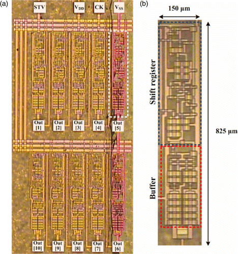
Figure 8. Measurement results of the proposed gate driver.
4. Conclusions
A gate driver composed of a shift register and an output buffer and using p-type LTPS TFTs was proposed. The shift register does not suffer from clock skew problems, and the burden of the interface has been reduced as only one clock signal was employed, without additional reference voltages. This shift register does not need an additional mask signal and additional circuits to avoid overlapping between the adjacent output signals, because the CK signal includes a mask signal. The proposed two-stage buffer shows a full-swing output without threshold voltage loss, due to the bootstrapping effect at the gate node of the pull-down transistor. The gate driver was fabricated on a glass substrate using the p-type LTPS TFT process, for the 3.31″ WVGA LCD panel, and worked successfully with only one clock signal. To reduce the power consumption of the proposed gate driver, its schematic diagram can be varied by replacing the p-type inverters used in the proposed circuits with another one. Although the proposed circuits suggest the solutions of area reduction and increased output range using only p-type TFTs, the power consumption of the circuit still has to be reduced so that the p-type LTPS TFT process will become more attractive in terms of circuit performance as well as cost benefit.
Notes
Parts of this work were presented in Proceedings of IMID 2010.
References
- Jackson , T. N. , Lin , Y.-Y. , Gundlach , D. J. and Klauk , H. 1998 . IEEE J. Sel. Topics Quant. Electron. , 4 : 100
- Park , S. H.K. , Hwang , C.-S. , Ryu , M. , Yang , S. , Byun , C. , Shin , J. , Lee , J.-I. , Lee , K. , Oh , M. S. and Im , S. 2009 . Adv. Mater. , 21, 678
- Ha , Y.-M. 2000 . SID’00 Tech. Dig. , : 1116
- Lin , C.-H. L.J.-R. , Lin , C.-C. , Chen , M.-D. and Chung , C.-F. 2004 . IDW ’04 Proc. , : 455
- Nam , W.-J. , Lee , H.-J. , Shin , H.-S. , Park , S.-G. and Han , M.-K. 2006 . Jpn. J. Appl. Phys. , 45 : 4389
- Jung , S.-H. , Nam , W.-J. , Han , C.-W. and Han , M.-K. 2003 . SID ’03 Tech. Dig. , : 1396
- Joynson , R. E. , Mundy , J. L. , Burgess , J. F. and Neugebauer , C. 1972 . IEEE J. Solid-State Circuits , 7 : 217