Abstract
Highly stable amorphous indium–gallium–zinc-oxide (a-IGZO) thin-film transistors (TFTs) were fabricated with an etch-stopper and via-hole structure. The TFTs exhibited 40 cm2/V s field-effect mobility and a 0.21 V/dec gate voltage swing. Gate-bias stress induced a negligible threshold voltage shift (Δ V th) at room temperature. The excellent stability is attributed to the via-hole and etch-stopper structure, in which, the source/drain metal contacts the active a-IGZO layer through two via holes (one on each side), resulting in minimized damage to the a-IGZO layer during the plasma etching of the source/drain metal. The comparison of the effects of the DC and AC stress on the performance of the TFTs at 60°C showed that there was a smaller Δ V th in the AC stress compared with the DC stress for the same effective stress time, indicating that the trapping of the carriers at the active layer–gate insulator interface was the dominant degradation mechanism.
Keywords:
1. Introduction
Amorphous oxide semiconductors (AOSs) are promising candidates for channel materials in thin-film transistors (TFTs) for large-area, transparent, and/or flexible flat-panel displays. AOS TFTs exhibit a superior field-effect mobility of >10 cm2/V s, which is sufficiently large for driving active-matrix organic light-emitting diode (AMOLED) displays and large-area active-matrix liquid crystal displays (AMLCDs), and operate at low voltages (<5 V) owing to their small gate voltage swing of ∼200 mV/dec Citation1 Citation2. The main research focus of late is to find a way to attain their improved long-term stability Citation3–7.
In this paper, highly stable amorphous indium–gallium–zinc-oxide (a-IGZO) TFTs fabricated on a glass substrate are demonstrated. Their stability is attributed to their via-hole and etch-stopper structure, which minimizes the damage to the a-IGZO layer during the TFT fabrication process. The impact of the thermal DC and AC stress on the performance of the TFTs was investigated to test the device stability.
2. TFT fabrication
shows a cross-sectional view of the a-IGZO TFTs that were used in this study. The TFTs have an inverted, staggered structure similar to that of the conventional a-Si TFTs, with an etch stopper and via holes. The via-hole structure is used to minimize the damage to the a-IGZO layer during the TFT fabrication process steps, such as source/drain metal formation, passivation, and a-IGZO etching.
Figure 1. Cross-sectional view of the inverted, staggered a-IGZO TFT with via holes and an etch stopper.
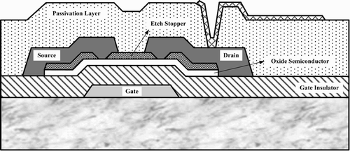
The fabrication process was as follows: a 60 nm thick Mo was deposited on glass and was patterned as the gate electrode, then a 200 nm SiO2 layer was deposited through plasma-enhanced chemical vapor deposition (PECVD) at 420°C, and a 20 nm a-IGZO layer (InO3:Ga2O3: mol%) was deposited through reactive sputtering at 200°C. To protect the a-IGZO layer from damage, a 100 nm SiO2 layer was deposited through PECVD at 200°C as an etch stopper. The SiO2 and a-oxide were then wet-etched to form an active layer island and via holes. After this, a 100 nm Mo was deposited and patterned as the source/drain electrode. Finally, a 200 nm SiO2 layer was deposited as the passivation layer, after which, via holes were formed and the Mo electrodes were patterned as shown in . The samples were annealed at 250°C in vacuum for 2 h as a post annealing step.
3. Results and discussion
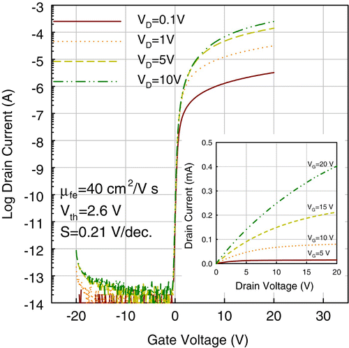
shows the transfer characteristics of the fabricated a-IGZO TFTs with 55 μm channel widths and 11 μm lengths. The saturation field-effect mobility extracted from the square root of the drain current ( when
was ∼40 cm2/V s at V
gs=15 V. The threshold voltage extracted from the linear extrapolation of
was ∼2.6 V. The gate voltage swing at V
ds=0.1 V was ∼210 mV/dec. The off-current values were below
A even at V
ds=10 V. The output characteristics (inset of ) showed no current crowding, indicating good ohmic contact.
Figure 2. The transfer and output (inset) characteristics of the a-IGZO TFTs.
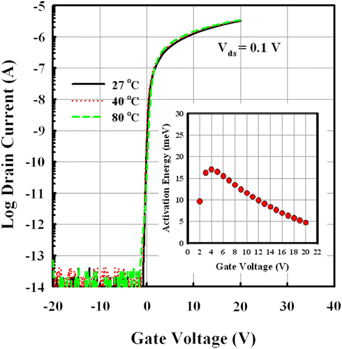
To check the thermal stability of the TFTs, the transfer characteristics were measured at different temperatures, from room temperature (RT) to 80°C. shows the results, which clearly indicate high thermal stability. The activation energy was extracted from the Arrhenius plot of log (I ds) versus the inverse of temperature, and the results are shown in the inset of . The activation energy was less than 20 meV, indicating that the Fermi level was very close to the conduction band and that the a-IGZO has a very steep tail-state distribution.
Figure 3. Transfer characteristics at different temperatures and the activation energy (inset) extracted from the Arrhenius plot of log (I ds) versus 1000/T.
The impact of the gate-bias stress on the performance of the a-IGZO TFTs was also investigated. shows the results of the application of the DC stress at RT. A DC gate bias of +20 V was applied for 5000 s while the source and drain electrodes were being grounded. The transfer characteristics barely changed after the application of the stress, indicating that the a-IGZO TFTs that were used in this study have high electrical stability. The same experiment was repeated for the AC stress, in which, an AC signal of 0–20 V, with a frequency of 5 kHz and a 50% duty ratio, was applied for 10,000 s while the source and drain electrodes were being grounded. A negligible change in the transfer characteristics was also observed at RT.
Figure 4. The transfer characteristics before and after the application of the DC stress at RT. The inset shows Δ V th as a function of the effective stress time (T s_eff) for the DC and AC stress at RT and 60°C. For the DC stress, the experimental stress time (T s) was the same as T s_eff. The AC pulse had a frequency of 5 kHz and a duty ratio of 50%. For the AC stress, T s_eff was thus equal to T s/2.
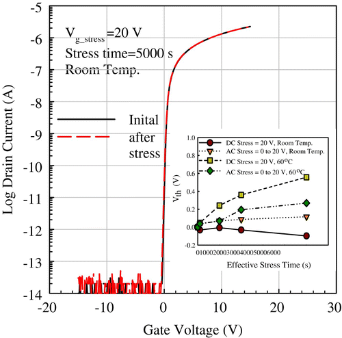
Change was observed only when the gate-bias stress-induced degradation was thermally activated. At 60°C, a small positive threshold voltage shift was observed after the application of either the DC or AC stress. The changes were still small, further confirming the electrical stability of the a-IGZO TFTs.
For a clearer analysis, the was plotted as a function of the effective stress time
at RT and 60°C, for the DC and AC stress, as shown in the inset of . For the DC stress, the experimental stress time (T
s) was the same as T
s_eff, and for the AC stress,
, because the duty ratio was 50%. At RT,
was almost negligible for either the AC or DC stress. At 60°C, however,
was approximately equal to 0.3 and 0.6 V after 5000 s effective stress time, respectively, for the AC and DC stress. This is a clear indication of charge trapping and detrapping during the application of the AC stress. The saturation mobilities and gate voltage swings of the TFTs showed no significant change after the application of either stress (AC or DC). This is due to the fact that the charge was trapped into the existing trap sites at the a-IGZO/SiO2 interface and/or bulk oxide semiconductor, without the generation of new traps. When the transfer characteristics were measured after the application of stress, the trapped charge (electrons) screened the applied electric field, thereby reducing the effective gate voltage. This is the reason for the positive
. It is also worth noting that the transfer characteristics can be recovered to the initial state by annealing at 250°C in vacuum for 2 h.
The of all the TFTs in this investigation is thus well described by the stretched-exponential equation Citation8
Citation9
In conclusion, highly stable, high-performance a-IGZO TFTs with an etch-stopper and via-hole structure were manufactured in this study to minimize the damage to the a-IGZO during the TFT fabrication process. The TFTs exhibited excellent device performance, with field-effect mobilities of 40 cm2/V s and gate voltage swings of 210 mV/dec. The thermal and electrical stability of these TFTs was also shown to be outstanding. While the device performance was unaffected by the DC and AC stress at RT, only a slightly positive threshold voltage shift was observed when the TFTs were stressed at 60°C. The shift is attributed to the charge trapping into the existing trap sites at the a-IGZO-SiO2 interface and/or bulk oxide semiconductor, without the generation of new traps.
Acknowledgements
This work was supported by the Industrial Strategic Technology Development Program (10035225, Development of a Core Technology for High-Performance AMOLED on Plastic) funded by MKE/KEIT.
References
- Hosono , H. 2006 . J. Non-Cryst. Solids , 352 : 851
- Hayashi , R. , Ofuji , M. , Kaji , N. , Takahashi , K. , Abe , K. , Yabuta , H. , Sano , M. , Kumomi , H. , Nomura , K. , Kamiya , T. , Hirano , M. and Hosono , H. 2007 . J. SID , 15 : 915
- Riedl , T. , Görrn , P. , Hölzer , P. and Kowalsky , W. 2007 . Phys. Stat. Sol. (RRL) , 1 : 175
- Lee , J.-M. , Cho , I.-T. , Lee , J.-H. and Kwon , H.-I. 2008 . Appl. Phys. Lett. , 93 : 093504
- Suresh , A. and Muth , J. F. 2008 . Appl. Phys. Lett. , 92 : 033502
- Lim , W. , Kim , S.-H. , Wang , Y.-L. , Lee , J. W. , Norton , D. P. and Pearton , S. J. 2008 . J. Vac. Sci. Technol. B , 26 : 959
- Park , J.-S. , Kim , K. S. , Park , Y.-G. , Mo , Y.-G. , Kim , H. D. and Jeong , J. K. 2008 . Adv. Mater. , 21 : 329
- Libsch , F. R. and Kanicki , J. 1993 . Appl. Phys. Lett. , 62 : 1286
- Lopes , M. E. , Gomes , H. L. , Medeiros , M. C.R. , Barquinha , P. , Pereira , L. , Fortunato , E. , Martins , R. and Ferreira , I. 2009 . Appl. Phys. Lett. , 95 : 063502
- Kim , M. , Jeong , J. H. , Lee , H. J. , Ahn , T. K. , Shin , H. S. , Park , J.-S. , Jeong , J. K. , Mo , Y.-G. and Kim , H. D. 2007 . Appl. Phys. Lett. , 90 : 212114
- Yabuta , H. , Sano , M. , Abe , K. , Aiba , T. , Den , T. , Kumoni , H. , Nomura , K. , Kamiya , T. and Hosono , H. 2006 . Appl. Phys. Lett. , 89 : 112123
- Chowdhury , M. D.H. , Migliorato , P. and Jang , J. 2010 . Appl. Phys. Lett. , 97 : 173506