Abstract
Efficient two-color-mixed white organic light-emitting diodes are presented herein by employing a sky-blue phosphorescent dopant of iridium(III)bis[4,6-(difluorophenyl)-pyridinato-N,C 2′]picolinate (FIrpic) and an orange phosphorescent dopant of bis(2-phenylquinoline)(acetylacetonate)iridium(III) (Ir(phq)2acac) on the emissive layer. Very stable color variation under Δ 0.02 until a 5000 cd/m2 brightness value was realized by efficient carrier control in a multi-stacked emitting layer of blue/red/blue colors. Maximum current and power efficiencies of 23.8 cd/A and 22.9 lm/W in the forward direction were obtained. With balanced emission from the two emitters, the white-light emission of high correlated color temperature of 7308 K and the Commission Internationale de I'Eclairage coordinates of (0.30, 0.33) were achieved.
1. Introduction
Organic light-emitting diodes (OLEDs) have been commercialized for mobile flat-panel displays while maintaining their tremendous achievements in this application Citation1. OLEDs have also attracted considerable attention for other potential applications, such as backlighting, next-generation lighting, and flexible displays. White organic light-emitting diodes (WOLEDs) have attracted much attention in recent years due to their potential use in the backlight unit of flat-panel displays, full-color displays, and solid-state lighting applications. Various approaches have been adopted to improve their performance, including the doping of several fluorescent or phosphorescent materials in a single emitting layer (EML) Citation2–6, the use of stacked OLEDs Citation7–9, down-conversion of blue light Citation10, and the use of a multi-EML structure doped with different color-emitting dopants Citation11–16.
In three-color-mixed WOLEDs, the issues of undesired chromaticity as well as the poor batch-to-batch reproducibility result in low-image-quality displays. These issues are minimized in two-color mixing by using an orange emitter complemented with a blue emitter to produce a white light implemented for the use of a combination of fluorescent/phosphorescent or phosphorescent/phos- phorescent emitters in doped OLEDs. Consequently, the demand for efficient true orange bright color for multiple-color displays and lighting purposes has significantly increased. Indeed, the interest in employing orange emitters in combination with blue emitters to achieve white-light emission with the simpler OLED architecture has recently spurred.
Another issue is the achievement of high efficiency in WOLEDs. A key requirement for achieving such high efficiency is that only electrically generated excitons must be employed for emission. Most studies focus on improving the quantum efficiency of WOLEDs Citation11 Citation17 Citation18. Chemical n- and p-doping in carrier transport layers is a prerequisite for the preparation of highly efficient organic-based devices Citation19–21. Improved charge injection through ohmic contact at the electrode interface and high conductivity through the doping effect are the main reasons for the low-operating-voltage characteristic. In addition, phosphorescent host–dopant systems have been considered to obtain high quantum efficiency due to the electrically generated singlet and triplet excitons.
This paper is based on highly efficient blue-device configuration as well as on material sets. A novel WOLED structure was designed by incorporating an orange dopant into the blue emissive layer to obtain white emissions. Using a high-triplet-energy carrier transport material, the simple p–i–n structure of WOLEDs was realized. In this p–i–n device configuration, a very low onset voltage of 3.0 V and a driving voltage of 4.6 V were achieved to obtain a brightness of 1000 cd/m2. Maximum current and power efficiencies of 23.8 cd/A and 22.9 lm/W in the forward direction were obtained.\enlargethispage{-3.7pc}
2. Experiments
Orange phosphorescent OLEDs (PHOLEDs) were fabricated using N,N′-di[4-(N,N′-diphenylamino) phenyl]-N,N′-diphenylbenzidine (DNTPD) as a hole transport material and bis(10-hydroxybenzo[h]quinolinato) beryllium (Bebq2) as an electron transport material. Bebq2 was also used as the host material for orange PHOLEDs. Tris[2-phenyl-4-methylquinoline)]iridium(III) (Ir(mphq)3), bis(2-phenylquinoline)(acetylacetonate)iridium(III) (Ir(phq)2 acac), and tris(2-phenylquinoline)iridium(III) (Ir(phq)3) were used as the orange dopants. To fabricate WOLEDs, 1,1-bis(4-methylphenyl)-aminophenyl-cyclo- hexane (TAPC) was used as a hole transport material, and 1,3,5-tris(m-pyrid-3-ylphenyl)benzene (TmPyPB) as an electron transport material. 2,6-Bis[3-(carbazol-9-yl)phenyl] pyridine (DCzPPy) was used as a host material for EML. MoO3 was used as a p-dopant, and Cs2CO3 as an n-dopant. Iridium(III)bis[4,6-(difluorophenyl)-pyridinato-N,C 2′]picolinate (FIrpic) was used as a blue dopant, and Ir(phq)2acac as a red dopant.
To fabricate OLED devices, clean 2.5×2.5 cm2 glass substrates pre-coated with a 150 nm thick indium tin oxide (ITO) layer with a sheet resistance of 10–12 Ω/square were used. The ITO glass was cleaned by sonification in isopropyl alcohol and then rinsed in deionized water. UV-ozone was finally irradiated in a chamber. The p- and n-doped layers were thermally co-deposited with different crucibles. The host was doped with the blue- and orange-emitting iridium complex materials. Finally, LiF and Al as the cathode were deposited in another vacuum deposition system without breaking the vacuum. The deposition rates of LiF and Al were 0.1 Å/s and 5–6 Å/s, respectively. The active area of the fabricated devices was 2×2 mm2. The current density–voltage (J–V) and luminance–voltage (L–V) of the PHOLEDs were measured using a Keithley SMU 238 and a Minolta CS-100A. The electroluminescence (EL) spectrum and Commission Internationale de I'Eclairage (CIE) color coordinates were obtained using a Minolta CS-1000A.
3. Results and discussion
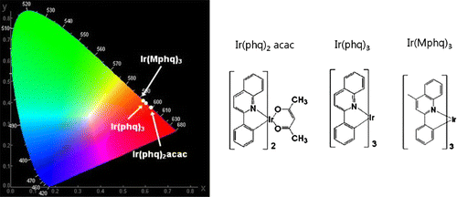
shows the molecular structure of three phosphorescent dopants, indicating their CIE coordinates in the diagram. The Ir(phq)2acac, Ir(phq)3, and Ir(mphq)3 orange dopants were used with the Bebq2 host. The Bebq2 host with a strong electron transport characteristic has the highest occupied molecular orbital (HOMO) energy of about 5.3 eV. The developed phosphorescent dopants, Ir(phq)2acac, Ir(phq)3, and Ir(mphq)3, have the HOMO energy levels at about 5.3, 5.2, and 5.1 eV, respectively, indicating that hole carriers can move without serious trapping by dopant molecules. Good electron transport is expected as the carrier trapping by the dopant molecules was almost negligible because of the narrow energy gap between the lowest occupied molecular orbital levels of the host (2.7 eV) and dopant (2.8–3.1 eV) molecules. In this host-guest system, the carrier movement by dopant molecules is almost negligible and doping concentration could minimize to consider the dopant-dopant self quenching issue. Therefore, the doping concentration condition was reduced as low as 3% in all PHOLEDs. DNTPD was used as a hole transport layer in the developed PHOLED configuration due to its good electron-blocking performance. Therefore, the available orange phosphorescent dopants were selected and phosphorescent orange OLEDs were fabricated. Three orange PHOLEDs were fabricated using three different red dopants. The device structures of the OLEDs that were fabricated for this study are as follows:
-
Device A: ITO/DNTPD (40 nm)/Bebq2:Ir(phq)2 acac (3 wt%, 30 nm)/Bebq2 (2 nm)/LiF (0.5 nm)/Al (100 nm);
-
Device B: ITO/DNTPD (40 nm)/Bebq2:Ir(phq)3 (3 wt%, 30 nm)/Bebq2 (2 nm)/LiF (0.5 nm)/Al (100 nm); and
-
Device C: ITO/DNTPD (40 nm)/Bebq2:Ir(mphq)3 (3 wt%, 30 nm)/Bebq2 (2 nm)/LiF (0.5 nm)/Al (100 nm).
Figure 1. Structures of different dopant materials, indicating the coordinates in the CIE diagram.
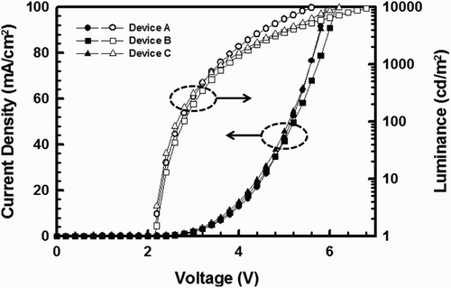
shows the J–V characteristics of the fabricated orange PHOLEDs. At the given constant voltage of 5.0 V, current density values of 43.01, 41.58, and 45.67 mA/cm2 were observed in the fabricated devices A, B, and C, respectively. The driving voltage to reach 1000 cd/m2 was 3.6 V for the devices A and B and was 3.4 V for device C. All the three devices showed similar J–V and L–V characteristics because of their similar HOMO and LUMO energy levels. A low turn-on voltage of 2.2 V was noticed in all the devices. In the developed orange OLEDs, such a low turn-on voltage is very difficult to achieve. In the described PHOLED configuration, the low driving voltage performances are attributed to the negligible charge trapping by the dopant molecules with no serious charge injection barriers at the heterointerfaces.
Figure 2. Current density–voltage (J–V) and luminance–voltage (L–V) plots of devices A, B, and C.
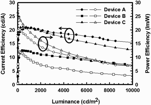
The current and power efficiency characteristics of the fabricated PHOLEDs are shown in . At the given constant luminance of 1000 cd/m2, the current and power efficiencies were 18.9 cd/A and 16.5 lm/W for device A, 11.9 cd/A and 10.4 lm/W for device B, and 21.3 cd/A and 19.7 lm/W for device C, respectively. These current efficiency data correspond to 17.0%, 10.2%, and 15.4% external quantum efficiencies of devices A, B, and C, respectively. Very high efficiency and good power efficiency results were obtained using these three orange dopants in the developed PHOLED configuration. The maximum current and power efficiencies were 19.0 cd/A and 21.8 lm/W for device A, 12.0 cd/A and 12.0 lm/W for device B, and 21.5 cd/A and 24.4 lm/W for device C, respectively. The best quantum efficiency was observed in device A.
Figure 3. Current and power efficiencies as functions of the luminance plot for devices A, B, and C.
Generally, triplet excitons have long diffusion lengths Citation11. Good confinement of triplet excitons within the emissive layers can be achieved when all the corresponding materials (i.e. the host materials and the adjacent hole transport material (HTM) and electron transport material (ETM)) have higher triplet energy levels than the triplet emitter. The triplet energy (T 1) levels of Ir(phq)2acac, Ir(phq)3, and Ir(mphq)3 were 2.0, 2.1, and 2.1 eV, respectively. In addition, the triplet energies (T 1) of TAPC, TmPyPB, DCzPPy, and FIrpic were about 2.8, 2.8, 2.7, and 2.6 eV, respectively Citation22–24. Based on their triplet energy alignments, it can be speculated that there should be an efficient exothermic energy transfer from DCzPPy triplet states to the FIrpic and Ir(phq)2acac dopant triplet states, as well as an excellent triplet energy confinement on the FIrpic molecules within the emissive layers. It is important to suppress any back-energy transfer from the guest triplet states to the others, and to enable the consumption of all the electrically generated triplet excitons contributing to the emission. Among the existing dopants, Ir(phq)2acac was selected as an orange dopant material because it generates a low driving voltage with high quantum efficiency.
Blue and orange phosphorescent dopants were incorporated into a single host to demonstrate a simple WOLED, which was fabricated using the p–i–n structure. DCzPPy was used as an electron transport single host, considering the very rapid electron movement from the anode. The fabricated white phosphorescent OLEDs are as follows:
-
Device D: ITO/TAPC: MoO3 (20%, 60 nm)/TAPC (10 nm)/DCzPPy:FIrpic (3%, 2 nm)/DCzPPy:Ir(phq)2 acac (2%, 2 nm)/DCzPPy:FIrpic (3%, 6 nm)/TmPyPB (10 nm)/TmPyPB:10% Cs2CO3 (25 nm)/Al.
shows the energy level diagram of this WOLED. The large difference in HOMO levels between TmPyPB and DCzPPy can effectively prevent hole leakage from the EML, while the high-lying LUMO levels of the 10 nm TAPC layer can act as an efficient barrier to the electron transport out of the EML. Therefore, both the charges and the generated excitons can be well confined within the EML to enhance the device efficiency. shows the device characteristics of the fabricated WOLEDs. The turn-on voltage of device D (1 cd/m2) was 3.0 V. A driving voltage (at 1000 cd/m2) of 4.6 was obtained. The TAPC and TmPyPB have higher carrier mobilities with high triplet energies, leading to effective hole and electron transport to the emissive layers Citation23. Moreover, a stepped progression of the HOMO and LUMO energy levels of the carrier transport materials and the host materials facilitated hole and electron injection into the emissive layers. The maximum current and power efficiencies of the WOLED were 23.8 cd/A and 22.9 lm/W. These values were achieved in the forward direction, without the use of any out-coupling technique.
Figure 4. Schematic representation of the device configuration.
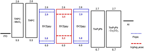
Table 1. Performances of WOLED.
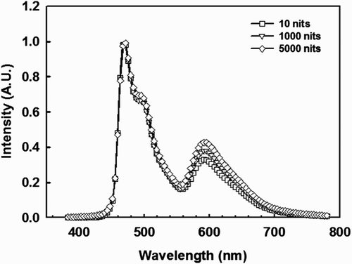
The EL spectra of the WOLED exhibited two characteristic peaks at about 470 and 598 nm, with a shoulder at 490 nm, as shown in . Such peaks or shoulder originated from those of the FIrpic and Ir(phq)2acac dopants, respectively. The CIE coordinates were found to be (0.30, 0.33), which are suitable for lighting application. Its color temperature and color-rendering index were 7308 K and 62, respectively. These CIE coordinates are sufficient to cover the high-color-temperature requirement, mimicking that of sunlight at noon. They are located near illuminant D65 (0.31, 0.33).
Figure 5. The EL spectra of the WOLED (device D).
4. Conclusions
A highly efficient WOLED with orange and sky-blue emitters was demonstrated. Low turn-on and operating voltages of 3.0 and 4.6 V at 1 and 1000 cd/m2, respectively, were obtained in the WOLED. The maximum current and power efficiencies were 23.8 cd/A and 22.9 lm/W, respectively. It was noted that the distinct emission nature of each dopant and the balanced charge injection and recombination within the EML are the key points for realizing high efficiency.
Acknowledgements
This work was supported by the Ministry of Knowledge Economy of the Republic of Korea.
References
- Lee , J. Y. , Kwon , J. H. and Chung , H. K. 2003 . Org. Electron. , 4 ( 143 )
- Kido , J. , Hongawa , K. , Okuyama , K. and Nagai , K. 1994 . Appl. Phys. Lett. , 64 ( 185 )
- D'Andrade , W. , Holmes , R. J. and Forrest , S. R. 2004 . Adv. Mater. , 16 ( 624 )
- Chuen , C. H. and Tao , Y. T. 2002 . Appl. Phys. Lett. , 81 ( 4499 )
- Shao , Y. and Yang , Y. 2005 . Appl. Phys. Lett. , 86 ( 073510 )
- Niu , Y. H. , Liu , M. S. , Ka , J. W. , Bardeker , J. , Zin , M. T. , Schofield , R. , Chi , Y. and Jen , A. K.-Y. 2007 . Adv. Mater. , 19 ( 300 )
- Kanno , H. , Holmes , R. J. , Sun , Y. , Kena-Cohen , S. and Forrest , S. R. 2006 . Adv. Mater. , 18 ( 339 )
- Guo , F. and Ma , D. 2005 . Appl. Phys. Lett. , 87 ( 173510 )
- Chang , C. C. , Chen , J. F. , Hwang , S. W. and Chen , C. H. 2005 . Appl. Phys. Lett. , 87 ( 253501 )
- Krummacher , B. C. , Choong , V.-E. , Mathai , M. K. , Choulis , S. A. , So , F. , Jermann , F. , Fiedler , T. and Zachau , M. 2006 . Appl. Phys. Lett. , 88 ( 113506 )
- Sun , Y. , Giebink , N. C. , Kanno , H. , Ma , B. , Thompson , M. E. and Forrest , S. R. 2006 . Nature , 440 ( 908 )
- Wang , Y. Z. , Sun , R. G. , Meghdadi , F. , Leising , G. and Epstein , A. J. 1999 . Appl. Phys. Lett. , 74 ( 3613 )
- Kim , C.-H. and Shinar , J. 2002 . Appl. Phys. Lett. , 80 ( 2201 )
- Cheon , K. O. and Shinar , J. 2002 . Appl. Phys. Lett. , 81 ( 1738 )
- Lei , G. , Wang , L. and Qiu , Y. 2006 . Appl. Phys. Lett. , 88 ( 103508 )
- Yu , X. M. , Kwok , H. S. , Wong , W. Y. and Zhou , G. J. 2006 . Chem. Mater. , 18 ( 5097 )
- Schwartz , G. , Reineke , S. , Rosenow , T. C. , Walzer , K. and Leo , K. 2009 . Adv. Funct. Mater. , 19 ( 1319 )
- Reinke , S. , Lindner , F. , Schwartz , G. , Seidler , N. , Walzer , K. , Lüssem , B. and Leo , K. 2009 . Nature , 459 ( 234 )
- Duan , Y. , Mazzeo , M. , Maiorano , V. , Mariano , F. , Qin , D. , Cingolani , R. and Gigli , G. 2008 . Appl. Phys. Lett. , 92 ( 113304 )
- Huang , J. , Huang , J. , Pfeiffer , M. , Werner , A. , Blochwitz , J. , Leo , K. and Liu , S. 2002 . Appl. Phys. Lett. , 80 ( 139 )
- Kanno , H. , Sun , Y. and Forrestet , S. R. 2005 . Appl. Phys. Lett. , 86 ( 263 )
- Jeon , W. S. , Park , T. J. , Kim , S. Y. , Pode , R. , Jang , J. and Kwon , J. H. 2009 . Org. Electron. , 10 ( 240 )
- Tanaka , D. , Takeda , T. , Chiba , T. , Watanabe , S. and Kido , J. 2007 . Chem. Lett. , 36 ( 262 )
- Su , S. J. , Chiba , T. , Takeda , T. and Kido , J. 2008 . Adv. Mater. , 20 ( 2125 )