Abstract
The mechanism for lattice-shaped mura defects was proposed by characterizing the electro-optic properties of liquid crystal (LC), which showed different transmission properties between the normal and mura defect areas. An increase in the mura defect rate was observed when the dotted LC in the one drop filling (ODF) was exposed for a longer time. The dotted LC droplet at the edge evaporated more rapidly than that in the center. This resulted in a higher concentration of polar singles at the edge of the dotted LC droplet, leading to a higher Δn value and higher transmittance. This implies that the reduction of the exposure time of the dotted LC to air plays a critical role in decreasing the occurrence of lattice-shaped mura defects in ODF.
1. Introduction
Thin-film-transistor liquid crystal displays (TFT-LCDs) with higher resolutions and larger panel sizes have been widely used of late to support full-featured multimedia Citation1. In LCD panel fabrication, the mura defect is known as a critical failure because its origins have not yet been definitively determined. The mura defect is closely related to the defects in a fixed gray scale and appears as a low contrast over the non-uniform luminance region Citation2–4. Most mura defects can be attributed to the non-uniform properties, such as the thickness, surface roughness, or liquid crystal (LC) electro-optic properties. Among these, it is most difficult to determine the root cause of the mura defect that takes place in the one drop filling (ODF) due to the deficiency of the pertinent analysis method.
ODF is one of the most important cell processes in the LCD production line for the assembly of the upper and lower glasses with an alignment accuracy of less than 3 μm Citation5. In this step, various kinds of mura defects have been reported, related with LC and polyimide Citation6–9. Thus, much effort has been exerted to find the origin of the mura defects that take place in the ODF step. It was found, however, that the relationship between the LC element composition and the formation of mura defects is not yet fully understood and is still being investigated. By analyzing the components of the specific regions showing different electro-optic properties, the origin of mura defects can be determined. To the best of these authors’ knowledge, however, no work has yet been conducted for this purpose.
In this work, the origin of mura defects related with the LC process was determined via electro-optical analysis, which showed different transmittance values during the process. Furthermore, the relevance of mura defects under vacuum conditions in ODF was investigated in the LCD mass production line. From these, defect-free conditions of the ODF process were proposed.
2. Results and discussion
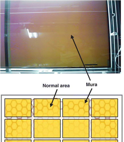
shows a photograph and schematic diagram of the lattice-shaped mura defects that were observed in the final test step of the LCD fabrication process. The locations of the lattice-shaped mura defects were closely related with the LC dotting positions. Various dotting patterns, such as rectangle and diamond, were examined to find their geometric effect on the mura defects. They were observed to be independent of the dotting patterns, however, which means that the mura defects did not originate from the geometric effect. Furthermore, the lattice-shaped mura defects were observed regardless of the driving bias, and the degree of mura defects was not changed by the bias condition. These imply that the mura defects that were observed can be attributed to the changes in the electro-optic or material properties after the ODF process.
Figure 1. Photograph and schematic diagram of the lattice- shaped mura defects observed in the final test step of the LCD fabrication process.
The cell gap heights between the normal and mura defect areas were evaluated using the Axoscan system. At the initial stage, the dotted LC had a normal symmetric shape, but after a few minutes, the areas that overlapped with the neighboring dotted LC increased, and the lateral size of the dotted LC also increased due to the spread of the dotted LC, as shown in . Therefore, it is important to check the influence of the agglomeration on the dotted LC around the edge of the dotting position.
Figure 2. (a) Schematic drawing of the LC droplet that flowed downward after dotting. (b) Change in the cell gap in the mura defect area as a function of the annealing time.
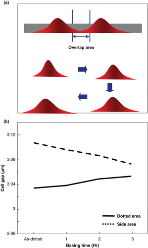
shows the change in the LCD panel cell gap as a function of the annealing time. In the as-dotted state, the cell gap height in which the mura defects were found was obviously higher than that of the normal position. Meanwhile, the cell gap difference between the dotted and normal areas was reduced after thermal annealing, which followed the assembly. The lattice-shaped mura defects, however, did not disappear, and no change in the degree of mura defects was observed even though the overlapped LC at the edge flowed downward. These indicate that the lattice-shaped mura defects had another cause, and that the overlapping of the LC at the edge was not the root cause of such phenomenon.
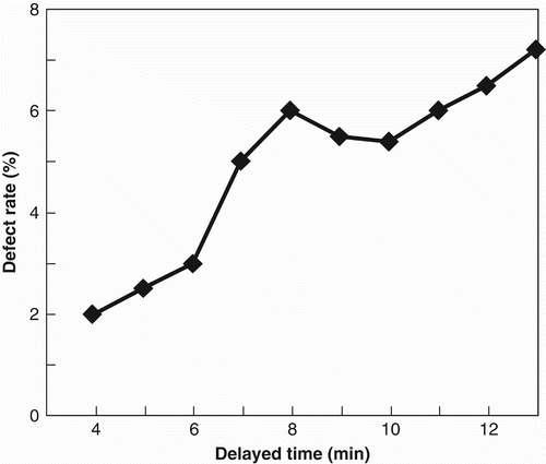
shows the defect ratio generated by the lattice-shaped mura defects with respect to the delay in the process time, in which the dotted LC was sealed during the assembly process. The LC was dotted at 1-min intervals, and the ODF process was conducted simultaneously. After that, the ratio of the lattice-shaped mura defects was monitored. The mura defect ratio soared upward as the process delay time increased. From these, it can be inferred that the exposure time of the dotted LC to air is closely related to the lattice-shaped mura defects in the ODF process.
Figure 3. Change in the lattice-shaped mura defect rate with LC exposure time to air during the ODF process.
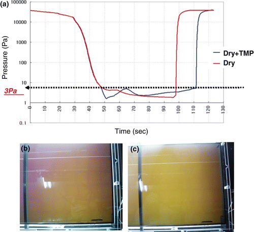
shows the change in vacuum pressure with the use of different pumping methods (i.e. dry-pump-only and dry-pump-plus-turbomolecular-pump (TMP) methods). The time for reaching the appropriate pressure of 3 Pa was shorter in the case of the dry-pump-only method. In the case of the dry-pump-plus-TMP method, it took much time to reach the designated pressure because the pumps must be operated sequentially. In the ODF process, the appropriate pressure is important because a relatively high pressure induces other kinds of defects, such as the formation of particles and bubbles. By reducing the time for reaching the operating pressure in the assembly step of ODF, the degree of lattice-shaped mura defects was reduced, as shown in (longer time to reach the operating pressure) and (shorter time to reach the operating pressure). This means that the lattice-shaped mura defects are closely related to the exposure time of LC to air in the ODF process.
Figure 4. (a) Change in vacuum with the different pumping methods of dry-pump-only and dry-pump-plus-TMP. The degree of lattice-shaped mura defects was reduced from the (b) dry-pump-only method to the (c) dry-plus-TMP method.
shows the change in the shape of the dotted LC droplet after its 600-s exposure to air. The LC droplet was flown downward with a long tail, after which, in the three areas of A, B, and C, the physical properties of LC were examined and were compared with the initial stage. These properties are summarized in . At the edge area (A), after 10-min exposure to air and the vacuum assembly process, the evaporation rate became faster than that in the other areas (B, C). This is due to the geometric effect (i.e. the evaporation rate is higher on a thin surface). Under these conditions, it was found that the polar single's concentration dramatically increased by about 18% due to the rapid evaporation of the monomer in the LC. Little change in the concentration at B and C was observed even after the same exposure conditions. Weight variation between the as-dotted and after-exposure conditions was found due to the fact that the extracted LC weight was slightly different at each extraction. The high concentration of the polar single means a higher Δn value Citation10. Thus, the difference in transmittance can be attributed to the relative difference in the polar single's concentrations.
Figure 5. Schematic illustration of the dotted LC droplet after 10-min exposure to air. The evaporation rate of the LC single at each area is different.
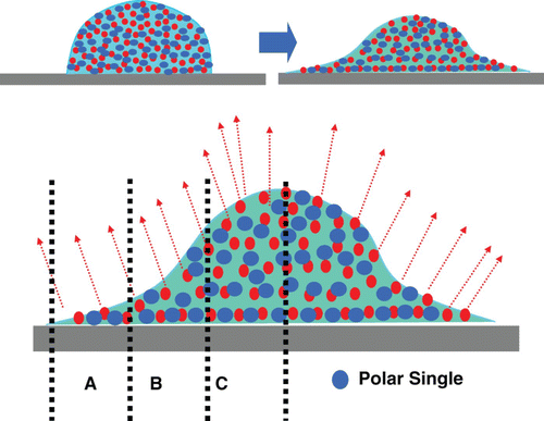
Table 1. Summary of the concentrations of the polar single and monomer before and after exposure to air.
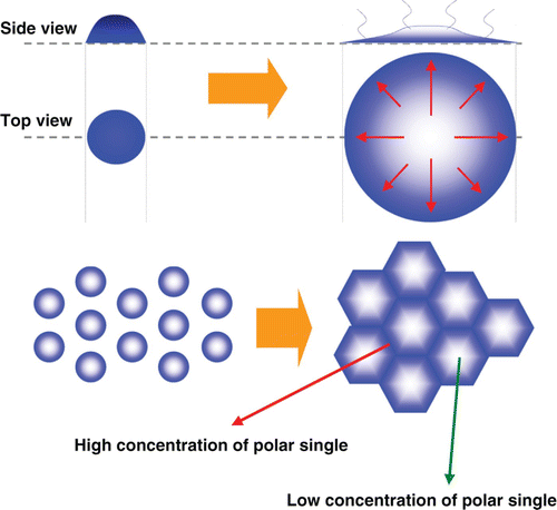
The mechanism for the lattice-shaped mura defect, deduced from the LC optical analysis, is schematically illustrated in . In the initial state, the dotted LC showed a normal symmetric shape, but due to the delay in the assembly and the exposure to vacuum, the LC droplet flowed downward. At this moment, at the edge area with a thin LC surface, the monomer evaporated at a higher speed, resulting in a higher concentration of polar singles compared with the center area. This led to a higher Δn value and higher transmittance. It can thus be inferred that much effort is needed to reduce the delay in the ODF process.
Figure 6. Side and top views of the dotted LC after exposure to air and after vacuum assembly in the ODF process. The high concentration of the polar single after the evaporation of the monomer caused the mura defect at the edge of the LC dotted area.
In the mass production line, about 1–2 min is needed to move the LC dotted glasses to the ODF equipment. The assembly process, however, generally takes 3–5 min, which shows that the control and reduction of the process time in the vacuum state is another critical factor in the reduction of the lattice-shaped mura defects. In the case of the vacuum condition, a high vacuum state has an advantage in that the air and particles can be easily removed. Much time is needed, however, to reach the high vacuum state, where lattice-shaped mura defects can easily occur. On the contrary, in the low vacuum state, air or bubbles can permeate during the assembly process, but the mura defect rate can decrease. It can be deduced from these that the control of the optimum vacuum state is essential in increasing the yield in the ODF process.
There has been a great demand of late for fast-response TFT-LCDs so as to reduce the blurring, which is the disadvantage of hold-type displays like TFT-LCDs. For the realization of a fast-response LCD panel, new LC materials must be prepared. The LC material for fast response, however, is highly volatile. It can thus be inferred that the mura defect originating from the evaporation difference among the areas will be more critical in the future. Therefore, it will be more important in reducing the exposure time of the dotted LC to air and vacuum.
3. Conclusion
In this study, the mechanism of the lattice-shaped mura defects generated in the LC ODF process was investigated. At the edge part of the dotted LC, the monomer highly evaporated, resulting in a higher concentration of polar singles compared with the center area, leading to a higher Δn value and higher transmittance. Based on these, the process factors influencing the mura defects were considered. The results of this study can be helpful in examining the relationship between transmittance and LC optical analysis.
References
- Park , H.-S. , Ji , S.-B. , Han , M.-K. , Lee , J.-S. , Kim , C.-W. and Choi , K.-S. 2009 . J. Soc. Inf. Display , 17 : 681
- Wang , P.-C. and Hwang , S.-L. 2009 . J. Soc. Inf. Display , 17 : 671
- Chen , C.-C. , Hwang , S.-L. and Wen , C.-H. 2008 . J. Soc. Inf. Display , 16 : 969
- Bo Wang , S. , Jhang , Z.-J. and Wen , C.-H. 2006 . SID Symposium Digest , 37 : 291
- Boer , W. 2005 . Active Matrix Liquid Crystal Displays: Fundamentals and Applications , Amsterdam : Newnes Elsevier .
- Fang , L.-T. , Chen , H.-C. , Yin , I.-C. , Wang , S.-J. , Wen , C.-H. and Kuo , C.-H. 2006 . Proc. SPIE , 6070 : 60700G
- Nakano , H. and Mori , Y. 2005 . Proc. SPIE , 5880 : 588013
- Mori , Y. , Tanahashi , K. and Tsuji , S. 2004 . Opt. Eng , 43 : 2696
- Mori , Y. , Yoshitake , R. , Tamura , T. , Moriguchi , K. , Tanahashi , K. and Tsuji , S. 2002 . Proc. SPIE , 4789 : 283
- Yeh , P. and Gu , C. 1999 . Optics of Liquid Crystal Display , New York : John Wiley & Sons . Chapter 1