Abstract
In this paper, the dynamic characteristics of the novel amorphous silicon thin-film transistor gate drive circuit applied on a 10.1-in. panel are optimized by using a multi-objective optimization method. Simultaneously, considering the multiple electrical characteristics of the tested circuit, the achieved results reveal interesting properties as well as good sensitivity of the optimized design parameters. The optimal specifications not only suppress the output ripple, but also reduce the dynamic and static power consumptions.
1. Introduction
In recent years, the panel circuit's design method has been a key technique for fabricating integrated amorphous silicon thin-film transistor (TFT) gate (ASG) driver circuits on glass Citation1–6 because of the elimination of the driver ICs, single with low-cost processes, compactness, and mechanical reliability. The topology of the ASG driver circuit, however, is requested to achieve a superior and stable output waveform and low power consumption. Therefore, dynamic characteristics are requested to meet the given specifications for ASG circuits. Various methods were reported to improve the performance of the circuits; among them, the empirically trial-and-error method was adopted by circuit designers to tune the circuit's parameters, such as the device geometry, biasing, and passive component Citation7 Citation8. Thus, the task of circuit design in display circuit manufacturing is time-consuming as it aims to meet all the specifications. From the computational engineering viewpoint, the evolutionary methods for optimal circuit design may benefit the display panel technology Citation2 Citation3 Citation5 Citation9. For example, a single-objective simulation-based genetic algorithm (GA) has been recently proposed for optimizing the device Citation2 Citation3 Citation5 Citation9; it can attain an astonishing result when it solves a problem that has a single-objective function. To optimize problems with multiple objective functions, one has to weight all the objectives and then calculate the averaged cost function. For a practical ASG circuit, however, it generally has to meet multiple design targets; consequently, the single-objective GA is probably not computationally effective for optimizing the circuit.
In this paper, the dynamic characteristic of the novel ASG drive circuit applied on a 10.1-in. panel is optimized by using a multi-objective evolutionary algorithm (MOEA). The proposed MOEA and a general TFT circuit simulator are integrated and implemented based on the environment of the unified optimization framework (UOF) Citation10 for the multi-objective ASG driver circuit design optimization. Notably, it has been confirmed that the UOF has excellent flexibility and extensibility to the optimal design of analog and digital circuits Citation10. Simultaneously, considering the multiple electrical characteristics, including the required targets [i.e. rise time (<3 μs), fall time (<2 μs), and ripple (<−5.5 V) of the tested circuit], the achieved results reveal interesting properties as well as good sensitivity of the optimized design parameters. The theoretically optimal specifications not only successfully suppress the output ripple (reducing it from the original specification of −3.02 to −7.17 V), but also reduce the dynamic power (14.5% reduction) and static power (9% reduction) consumptions, respectively. The optimized ASG driver circuit together with the associated parameters are used for sample fabrication to verify the optimal design. The results of the measured sample meet the design criteria. Notably, the measured ripple of the sample is −6 V, which is significantly less than that of the required specification of −5.5 V.
This paper is organized as follows. In Section 2, the studied circuit topology, the associated optimization problem, and the developed optimization method are briefly described. In Section 3, the achieved results, including optimization and measurement, are reported. Finally, the conclusions of the study are presented.
2. Circuit and optimization method
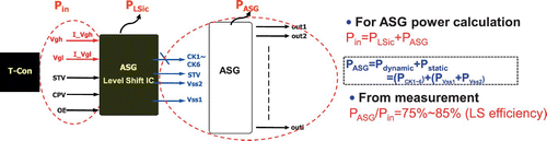
The block diagram and operation of the ASG driver circuit are briefly described, and the associated optimization problem is stated. The tested ASG driver circuit in this work consists of 21 design parameters, which include the devices’ sizes and the capacitance's dimensions, as shown in . In general, the circuit consists of the following blocks: the pull-up control, pull-down control, pull-up output, and pull-down output circuits. The pull-up control circuit contains three devices and one capacitor. The pull-down control circuit contains 10 devices and 2 capacitors. The pull-down output circuit contains three devices and uses the next-stage output signal (Out n+2) and the Clock_in and Reset signals to trigger the transistor to stabilize the output. The pull-up output circuit contains one device and one capacitor; in particular, TFT M12 is the most important device of the ASG circuit. Sensitivity analysis of the optimized characteristics for the M12 was performed to find a robust solution for the tested circuit. In addition, the whole charge action can be described; the pull-up control circuit can pre-charge the X node simultaneously, and then the output signal OUT n and trigger signal (STV n ) are raised to V H with the help of the boost-up. In this time slot, X exceeds V H. The important electrical characteristics – the rise time, fall time, ripple, and power dissipation – are significant for evaluating the performance of the specified design. In real-world applications, these characteristics are not only requested to meet the given specifications for the improved quality of the display panels, but are also expected to minimize the power dissipation for performance improvement. The power dissipation is defined as shown in , where the total input power (P in) is equal to the sum of the power of Level Shift IC (P LSic) and the power of the ASG circuit (P ASG). The P ASG can be further divided into the dynamic power (P dynamic) and the static power (P static). The P ASG can be estimated by measuring P in empirically, where the P ASG is 75–80% of the P in.
Figure 1. (a) The ASG circuit architecture. Each ASG stage (b) contains four-part circuits (c), including the pull-up control, pull-down control, pull-up output, and pull-down output circuits. (d) The timing chart shows the clock signals and the first-stage signals. Notably, for the different power supplies, such as Vss1 and Vss2, they are used to make the voltage stable and the power dissipation lower.
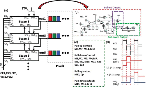
Figure 2. From experience, the P ASG can be estimated to be 75–80% of the P in.
The authors’ target is to achieve the aforementioned specifications for manufacturing cost-effective ASG circuits. The rise time, fall time, and ripple were first chosen among the multiple objective functions for minimization, where each parameter to be optimized and the objective functions have their own constraints. In the model problem, the width of each active device was optimized, where the search range of each device was defined by empirical assignment and the evaluation task was conducted by running an external circuit simulator.
In the following simulations, V H, V ss1, and V ss2 are set to 26.5, −5.5, and −10 V, respectively, the row line load is approximated by a six-stage RC circuit, and the length of each TFT is fixed at 4.5 μm, except the TFT M8, which is fixed at 6 μm. and show the TFT circuit simulator simulated results of the original and optimized designs. The rise time is defined by the time interval required to raise the leading edge of the pulse from 10% to 90% in the peak pulse amplitude, and the definition of the fall time is contrary to that of the rise time. The ripple of the output node, denoted as “ripple-X,” is defined by the maximum voltage level after the desired pulse. In addition to the above characteristics, special attention is paid to the ripple of the X node. It was found that the original specification shows a promising property for the rise and fall times, but that the ripple-X is poor. Below is a description of the implemented MOEA optimization system running on the UOF.
Figure 3. The optimization result (the red solid line) represents the optimized results showing similar rise and fall times compared with the original specification (the blue dashed line), but the optimized results can successfully decrease the output ripple.
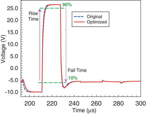
Table 1. Comparison of the required target, the original specification, and the optimized result
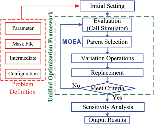
The implemented UOF system, as shown in , is an objective-oriented optimization framework for the problem of the ASG driver circuit design optimization. First, the files for the problem definition were prepared. Then, the files were put into the UOF system. The adopted technique integrates a MOEA and a numerical circuit simulator (for example, Eldo® was used to simulate the ASG circuit) running on the UOF, which is used to optimize the dynamic properties of the tested ASG circuit. The UOF provides basic interfaces to define a general problem and a generic solver, enabling these two different tasks to be bridged Citation10. The components of the UOF can be separated into problem and solver components. These two parts work independently, allowing a high-level code to be reused and rapidly adapted to new problems and solvers. The UOF design has a robust advantage in that the embedded simulators can be changed and used by other engineering applications. For example, it has been used in the semiconductor process, device optimization, and in circuit design problems in the authors’ recent studies Citation11–13.
Figure 4. The implemented UOF architecture for the ASG driver circuit design optimization. The entire system has two parts: the problem definition and the solver, which uses the MOEA in this work.
In contrast to the conventional GA, the adopted MOEA is a population-based multi-objective optimization method Citation14–17. With the mechanics of simulated natural behavior, including mutation, selection, and recombination, MOEA can select the individual relatively better solutions, and then the recombination operator is applied to generate new offspring. The mutation operation may change the individual in the offspring. Through the operation of mutation, the MOEA can reach the global solution. The operation iterative is taken until the stop criteria are achieved. As the multi-objective problem has to be solved, the selection operation is modified to solve the multi-objective problem through non-dominating sorting Citation18. As the MOEA can find the Pareto front on the objective space, it can obtain an excellent spread of solutions. Decision-makers can choose the solution according to their requirements. For robustness investigation, the sensitivity of the optimized parameters of the tested ASG driver circuit was verified. Sensitivity analysis is a method that can examine the influence of each parameter of the circuit design Citation5
Citation19. It is an important strategy applied on the present circuit design to verify how the small changes in the fabrication affect the electrical characteristics. The method varies the parameter within a small region, then the relationship between the optimized results and each parameter can be investigated and can enable the selection of the solution with the lowest sensitivity to avoid process variation. For the ASG driver circuit, the sensitivity of the intrinsic parameter is analyzed by varying the width of each device by 50% (±50%). The normalized sensitivity (Z
i
) for the aforementioned characteristics, including the rise time, fall time, and ripple, are calculated using the formula for each design parameter x
i
. The f
0 (x*) and
are the nominally optimized and perturbed results with respect to the interested parameter x*. Therefore, it can be varied within a small region by a differential.
3. Optimization and experiment results
compares the original and optimized designs, and lists the optimized parameters. The optimization results not only confirm all the requirements, but also exhibit more comparative considerations compared with the original design. The optimized circuit reduced the total width of all the TFTs (an about 11.6% reduction, from 9980 to 8820 μm). As shown in , the output current indicates that the optimized result has better performance in terms of power consumption. The most important achievement is that it successfully minimizes the C total, which causes a 14.5% reduction in the dynamic power consumption (from 420.00 to 358.89 μw) by fcv 2. As shown in , the optimized output current in the time frame from 2.6 to 2.9 μs was suppressed compared with the original one. The 9% reduction of the maximum leakage current was observed as listed in . Both results show that the optimized ASG driver circuit has very low static power consumption by IV, where V is the static voltage.
Figure 5. The output current shows that the optimized result has a better performance in terms of power consumption.
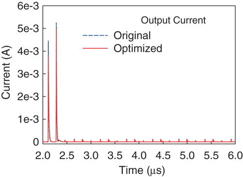
Figure 6. The zoom-in plot from . The optimized output current in the steady state can actually be suppressed, where the time frame is from 2.6 to 2.9 μs.
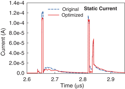
Table 2. List of original and optimized parameters
Table 3. Comparison of the maximum leakage currents between the original specification and the optimized result
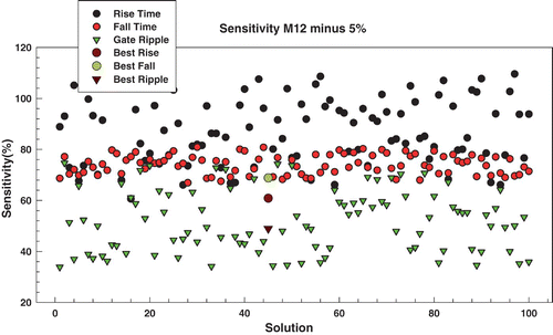
The sensitivity of the optimized parameter, particularly for the TFT M12, was evaluated, as shown in and . The TFT M12 and M13 govern the output voltage, but the TFT M12 is the most important transistor as it supplies the pixel's voltage, while the TFT M13 supplies the STV's voltage. Thus, the TFT M12 has the largest transistor width and affects the total sensitivity. If f 0 (x*) represents the characteristic of the analysis point (i.e. the nominal case), the sensitivity of f 0 in x* with respect to x i can be calculated using Z i , as shown in the previous section. and show the calculated sensitivity with the +5% and −5% widths of the optimized devices, respectively. The figure reveals only the characteristics, with significant variation, excluding the ripple-X. The TFT M12 governs the charge ability to the OUT n and STV n nodes. The magnitude of sensitivity was found to be around 80%. This implies that the variation of M12’s width seriously affects the circuit's dynamic characteristics. Consequently, the TFT M12 was focused on because it possesses the largest sensitivity among all the parameters. As marked in and , the lowest sensitivity solution can be chosen for the rise time, fall time, and ripple, respectively.
Figure 7. The sensitivity analysis for each solution with respect to the TFT M12 for the nominal width has +5% variations.
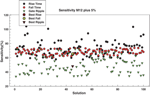
Figure 8. The sensitivity analysis for each solution with respect to the TFT M12 for the nominal width has -5% variations.
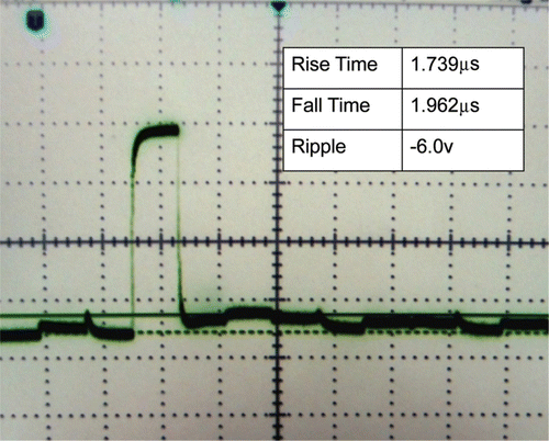
To verify the feasibility of the optimized ASG driver circuit, one of the optimized solutions was selected for the sample fabrication, and characterization was performed. shows the layout picture of the sample to be fabricated. is an optical image of the fabricated ASG driver circuit obtained from the scanning electron microscope (SEM). The measured data are shown in . The measured rise time of the fabricated sample is superior to the theoretically stimulated data. As summarized in the inset of , all the concerned electrical characteristics are within the design specifications. The achieved results and adopted optimization method have demonstrated the practicability of the proposed ASG driver circuit.
Figure 9. Layout plot of the fabricated sample of the optimized circuit.
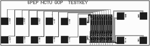
Figure 10. SEM optical image of the fabricated sample of the optimized circuit.
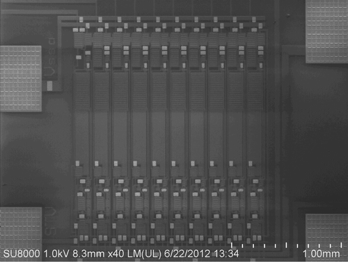
Figure 11. Measurement result showing that the optimized circuit is promising for production optimization. The performance is worse than that in . This may be due to the human operation and the quality of the testing load. It can be seen, however, that the output ripple is still lower than the origin. The ripple shows the stability of the ASG driver circuit.
4. Conclusions
The ASG driver circuit was optimized using the integrated optimization solver, based on a circuit-simulation-based MOEA in UOF. Via sensitivity analysis, the most critical parameter in the ASG driver circuit design was found. Promising dynamic characteristics, including low power consumption and high stability, were successfully achieved via both simulation and measurement. This optimization methodology is currently being applied for Indium Gallium Zinc Oxide (IGZO) TFT gate driver circuit design optimization.
Acknowledgements
This work was supported in part by Chimei-InnoLux Display Corp., Miao-Li, Taiwan, under a 2009–2012 grant.
References
- Shen , C.-H. , Lo , I. H. , Lin , P.-J. and Li , Y. KINTEX , Seoul , Korea. Technical Digest of International Meeting on Information Display , pp. 245 – 246 .
- Cheng , H.-W. , Huang , H.-M. , Li , Y. , Tsai , T.-C. , Chen , H.-Y. , Huang , K.-Y. and Hsieh , T.-H. KINTEX , Seoul , Korea. Technical Digest of International Meeting on Information Display , pp. 968 – 971 .
- Lin , P.-J. , Lo , I. H. , Li , Y. and Shen , C.-H. KINTEX , Seoul , Korea. Technical Digest of International Meeting on Information Display , pp. 78 – 79 .
- Li , Y. , Hwang , C.-H. , Chen , C.-L. , Yan , S. and Lou , J.-C. 2008 . IEEE Trans. Electron Dev. , 55 : 3314 – 3318 . (doi:10.1109/TED.2008.2005133)
- Li , Y. , Li , K.-F. , Lo , I. H. , Chiang , C.-H. and Huang , K.-Y. 2011 . J. Disp. Technol. , 7 : 274 – 280 . (doi:10.1109/JDT.2010.2102336)
- Lin , C.-L. , Cheng , M.-H. , Tu , C.-D. and Chuang , M.-C. 2012 . IEEE Electron Dev. Lett. , 33 : 679 – 681 . (doi:10.1109/LED.2012.2188269)
- Hong , S.-I. , Nam , K.-S. , Jung , Y.-H. , Ahn , H.-A. , In , H.-J. and Kwon , O.-K. 2012 . J. Inform. Disp. , 13 : 73 – 82 . (doi:10.1080/15980316.2012.674982)
- Jeong , J. Y. and Hong , M. P. 2008 . J. Inform. Disp. , 9 : 1 – 7 . (doi:10.1080/15980316.2008.9652055)
- Li , Y. , Lee , K.-F. , Lo , I.-H. , Chiang , T. , Huang , K.-Y. and Hsieh , T.-H. KINTEX , Seoul , Korea. Technical Digest of International Meeting on Information Display , pp. 114 – 115 .
- Li , Y. , Yu , S.-M. and Li , Y.-L. 2008 . Math. Comp. Simulat. , 79 : 1137 – 1152 . (doi:10.1016/j.matcom.2007.11.001)
- Li , Y. 2009 . Appl. Math. Comput. , 209 : 57 – 67 . (doi:10.1016/j.amc.2008.06.015)
- Li , Y. 2010 . Math. Comput. Model. , 51 : 944 – 955 . (doi:10.1016/j.mcm.2009.08.017)
- Li , Y. and Yu , S.-M. 2007 . IEEE Trans. Semicond. Manuf. , 20 : 432 – 438 . (doi:10.1109/TSM.2007.907623)
- Deb , K. 2001 . Multi-objective optimization using evolutionary algorithms , UK : Wiley, Chichester .
- Kim , J.-H. , Han , J.-H. , Kim , Y.-H. , Choi , S.-H. and Kim , E.-S. 2012 . IEEE Trans. Evol. Comput. , 16 : 20 – 34 . (doi:10.1109/TEVC.2010.2098412)
- Bosman , P. A.N. 2012 . IEEE Trans. Evol. Comput. , 16 : 51 – 69 . (doi:10.1109/TEVC.2010.2051445)
- Schutze , O. , Esquivel , X. , Lara , A. and Coello , C. A.C. 2012 . IEEE Trans. Evolut. Comput. , 16 : 504 – 522 . (doi:10.1109/TEVC.2011.2161872)
- Deb , K. , Pratap , A. , Agarwal , S. and Meyarivan , T. 2002 . IEEE Trans. Evolut. Comput. , 6 : 182 – 197 . (doi:10.1109/4235.996017)
- Williams , S. and Varahramyan , K. 2000 . IEEE Trans. Semicond. Manufact. , 13 : 208 – 218 . (doi:10.1109/66.843636)