Abstract
Flexible organic light-emitting diodes (OLEDs) are considered the next-generation displays. To realize stable and high-performance flexible OLEDs, inverted OLEDs (iOLEDs) integrated into oxide thin-film transistors are desired for active-matrix OLEDs. Unfortunately, however, the efficiency of iOLEDs has not been as good as that of the conventional OLEDs up to recent years, due to the difficulties in electron injection from the bottom cathodes to the organic layers in iOLEDs. In this paper, electron injection and transport are described to explain how to enhance the efficiency of iOLEDs. Various methods of improving the electron injection from the bottom cathodes to the organic layers are reviewed, especially focusing on the n-doping technology. The importance of the n-electron-transporting layer (ETL)/undoped ETL homo- and hetero-junction for efficient iOLEDs is also explained. Finally, the p–n junction is introduced as a new kind of electron injection layer that works very well independently of the cathode materials.
1. Introduction
The performance of organic light-emitting diodes (OLEDs) has significantly improved in the last 25 years, and they have been successfully launched in small electronics, such as MP3 players, cameras, and mobile phones. There are now major efforts to develop technologies toward large TVs and solid-state lightings. Beyond the replacement of the previous displays, OLEDs can open new fields, which can hardly be realized with the previous displays. One of the representative examples of the new technology is a flexible display, defined as a display that is stable against an external load for shape transformation, such as repeated bending, twisting, rolling, or folding.
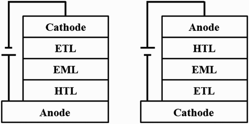
To demonstrate the high-performance flexible OLEDs, the main parts of the conventional OLEDs must be significantly modified. First of all, the brittle glass substrate must be replaced with flexible materials. Plastic, metal foil, and thin glass can be candidates for flexible substrates. Among them, plastics are the best candidate for flexible substrates due to their flexibility, low price, transparency, thickness, flat surface morphology, and light weight. Unfortunately, however, plastic substrates are particularly susceptible to damage under a high processing temperature. As such, oxide thin-film transistors (TFTs), which have a low processing temperature, flexibility, high carrier mobility, good uniformity, and improved stability, are favorable for the active-matrix circuit. As oxide TFTs are n-type in nature, inverted OLEDs (iOLEDs) composed of a bottom cathode, an electron-transporting layer (ETL), an emitting layer (EML), a hole-transporting layer, and a top anode from beneath, with the inverse deposition sequence shown in , can be more beneficial for the design of the backplane compared with the conventional OLEDs. If the conventional OLEDs are connected in series with oxide TFTs, however, a voltage-controlled current source configuration, which is essential to the stability of the device, cannot be achieved, and the current flow to the OLEDs will hardly be controlled by the transistor voltage Citation1. This problem can be solved by connecting an iOLED to the drain end of the n-type TFTs.
Figure 1. Device structures of the conventional OLED and the iOLED, respectively.
The main challenge associated with iOLEDs is the electron injection from the bottom cathode to the ETL, because there are limited stable cathode and electron injection materials that can be chosen from, for efficient electron injection contact. Various methods have been suggested to address this problem, including modification of the electrode work function Citation2–11, insertion of an interfacial layer Citation12–19, and interfacial doping Citation6,Citation20–29 in the electron injection layers (EILs). In this paper, methods of enhancing the electron injection will be described in detail, particularly focusing on the interface between the bottom cathode and the organic layer as well as the organic and organic (O/O) junctions, for high-performance inverted devices.
2. Issues of electron injection for iOLEDs
iOLEDs are classified into bottom and top emission OLEDs according to the direction of the light emission with respect to the substrate. The bottom emission iOLEDs are composed of substrate/transparent cathode/organic layers/opaque metal anode, and the lights are emitted through the bottom substrate. Indium-tin-oxide (ITO) is a preferred choice as the transparent bottom cathode for the bottom emission iOLEDs. In contrast, the top emission iOLEDs require an opaque metal cathode and a transparent anode, where metals such as Al or Ag can be used as the cathode. In addition, the Ag/ITO or Al/ITO composite can be used as the cathode for the top emission iOLEDs. The first iOLED, introduced by Baigent et al. Citation30, was a top emission OLED using a high-electron-affinity conjugated polymer, Cyano-Polyphenylene Vinylene (CN-PPV), on an aluminum cathode.
Even in the conventional OLEDs, electron injection was one of the most important issues for balancing the hole and electron injection, and consequently, for improving the efficiency of the devices. The research on the hole injection from the ITO into the organic layer was improved by using various hole-transporting materials to achieve almost ohmic behavior even in the early stage of the OLED research Citation31. In a similar way, ohmic-like electron injection contact was achieved using low-work-function metals such as Yb, Sm, Ca, and Mg Citation32 Citation33. These materials, however, have a stability issue due to the high reactivity coming from their low-work function. An alternative method is to insert alkali metals (Li and Cs) between the aluminum cathode and the organic layer, or alloying them with an Al cathode Citation34–37. Along with these methods, organic or inorganic compounds such as LiF, Li2O, NaCl, and KCl were additionally inserted as an interfacial layer to enhance the electron injection Citation38–43. The interfacial layer reduced the electron injection barrier by modifying the interfacial dipole, significantly increasing the efficiency of the device. The insertion of an LiF thin layer between the Al cathode and the ETL is one of the most widely used methods for good electron injection in the conventional OLEDs because it is easy to use and has good electron injection characteristics and stability. Unfortunately, however, the LiF thin layer is not a proper EIL for the iOLED. Heil et al. Citation44 reported that the electron injection characteristics of a thin LiF interlayer depend on the deposition sequences through the use of a single carrier device composed of LiF, Alq3, and Al. The current density–voltage (J–V) characteristics of the two different devices in showed significantly different behaviors. More than three orders of magnitude higher currents were obtained at a fixed voltage in the device where the LiF/Al was deposited onto the Alq3 layer than in the device where the Alq3 layer was deposited on top of the LiF/Al electrode. This difference is attributed to the decomposition of LiF into Li and F during the deposition of Al. The liberated Li acted as a dopant in the Alq3 layer, increasing the current density, similar to the use of a doping layer. This occurred only in the case of the top contact: ITO/Alq3/LiF/Al. A similar result was reported by another group Citation45. Recently, a highly efficient iOLED with an LiF bottom contact was reported Citation46, but this is a very limited case. Therefore, methods of enhancing the electron injection must be developed, for efficient iOLEDs. As the work function of Al or Ag is smaller than or close to that of ITO, good electron injection to the organic layers is most difficult to achieve with electron injection from the ITO cathode. As such, this paper focuses on electron injection from the ITO cathode.
Figure 2. J–V characteristics of electron-only devices depending on the different deposition sequences of a thin LiF interlayer. [Reprinted with permission from Heil et al. Citation44, © 2001, American Institute of Physics.]
![Figure 2. J–V characteristics of electron-only devices depending on the different deposition sequences of a thin LiF interlayer. [Reprinted with permission from Heil et al. Citation44, © 2001, American Institute of Physics.]](/cms/asset/b7523f5c-414f-41ae-bcde-cafdfa3eccf8/tjid_a_779324_o_f0002g.jpg)
3. Methods of enhancing electron injection in iOLEDs: adjustment of the energy barrier between the cathode and the organic interface
As discussed in the previous section, the LiF interfacial layer does not work properly as an EIL in iOLEDs. Instead, other materials, such as alkaline metal compounds, alkali metals, polymer, and self-assembled monolayers, are used to directly modify the work function of the bottom cathode [2–18,34–38,40–43,47,48]. Furthermore, electrical doping of alkali metals or metal carbonates in an organic material is also widely used Citation6,Citation19–27. Doping in organic semiconductors can increase the carrier density of the organic layers, thereby also increasing the conductivity of the doped layers Citation49–52. Energetically, electrical doping in the organic layers induces the vacuum level shift due to the interfacial dipoles at the interface between the metal or ITO and the organic layer, and reduces the thickness of the depletion layer near the metal or ITO electrode due to the band bending in the organic layers. As a result, the charge carrier injection is improved via tunneling through the depletion layer. These characteristics were analyzed via ultraviolet photoemission spectroscopy (UPS) measurement Citation53–67 or the kelvin probe (KP) method Citation68–73, and were also interpreted through capacitance–voltage (C–V) measurements Citation74 Citation75, as shown in . Electrically, it reduces the contact resistance between the metal and the organic layer, resulting in the lowering of the driving voltage and in the enhancement of the power efficiency of the OLEDs.
Figure 3. Energy level diagrams of doped organic layers obtained via (a) UPS, (b) KP, and (c) C−V measurements, respectively. [Reprinted from Blochwitz et al. Citation57, © 2001, with permission from Elsevier; Kröger et al. Citation73, © 2007 by American Physical Society; and Lee et al. Citation74, © 2012, Wiley-VCH.]
![Figure 3. Energy level diagrams of doped organic layers obtained via (a) UPS, (b) KP, and (c) C−V measurements, respectively. [Reprinted from Blochwitz et al. Citation57, © 2001, with permission from Elsevier; Kröger et al. Citation73, © 2007 by American Physical Society; and Lee et al. Citation74, © 2012, Wiley-VCH.]](/cms/asset/eee35ed6-a939-444e-b302-6a17b066f702/tjid_a_779324_o_f0003g.gif)
The energy barrier at the metal and organic (M/O) interface is also controlled by changing the orientation of the organic material and the interaction energy at the M/O interface, as shown in Citation76–86. Individual organic molecules generally have their own energy levels of the highest occupied molecular orbital and lowest unoccupied molecular orbital. Interestingly, however, the energy levels of organic molecules are modified depending on the molecular orientation (i.e. depending on their growth on the metal substrate) Citation76–86. In addition, a different molecular orientation modifies the carrier mobility of the organic layer, allowing the carrier injection and transport to be controlled at the same time, by using this method.
Figure 4. Change in the energy barrier at the M/O interface by controlling the orientation of the organic material. Energy level diagram for the (a) standing-6T/standing-DH6T/lying-DH6T-monolayer/Ag(111) structure, and (b) ITO/ZnPc/C60 and ITO/CuI/ZnPc/C60. [Reprinted from Duhm et al. Citation82, © 2008, with permission from Macmillan Publishers, Ltd. and Kim et al. Citation86, © 2013, with permission from Elsevier.]
![Figure 4. Change in the energy barrier at the M/O interface by controlling the orientation of the organic material. Energy level diagram for the (a) standing-6T/standing-DH6T/lying-DH6T-monolayer/Ag(111) structure, and (b) ITO/ZnPc/C60 and ITO/CuI/ZnPc/C60. [Reprinted from Duhm et al. Citation82, © 2008, with permission from Macmillan Publishers, Ltd. and Kim et al. Citation86, © 2013, with permission from Elsevier.]](/cms/asset/4401ffe2-29be-4718-a645-0a4469a38aff/tjid_a_779324_o_f0004g.jpg)
4. Importance of an energy barrier at the O/O interface in iOLEDs
4.1. Doped/undoped organic homo-junction
The energy barrier not only at the M/O interface but also at the O/O interface should be considered to achieve efficient electron injection and transport, because there is an intrinsic ETL between the n-ETL and the EML to prevent exciton quenching by the n-dopant at the n-ETL/EML interface when the n-ETL and EML are directly contacted.
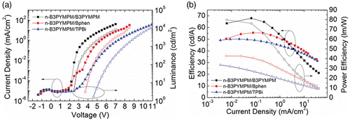
Recently, Lee et al. Citation27 reported the importance of the energy barrier between the n-doped ETL and the undoped ETL (i.e. organic homo-junction in iOLEDs). They used the n-i-p device structure with three different ET materials: bis-4,6-(3,5-di-3-pyridylphenyl)-2-methylpyrimi-dine (B3PYMPM), 4,7-diphenyl-1,10-phenanthroline (Bphen), and 2,2′,2′′-(1,3,5-benzenetriyl) tris-[1-phenyl-1H-benzimi- dazole] (TPBi), respectively. The performances of the devices are shown in and are listed in . Among the three devices, that with the B3PYMPM homo-junction showed the highest maximum external quantum efficiency (EQE; 20%) and the lowest injection and turn-on voltage, as shown in , even though the mobility of the pristine B3PYMPM layer is one order of magnitude lower than that of Bphen.
Figure 5. Device performances of three different iOLEDs, using the B3PYMPM, Bphen, and TPBi homo-junctions, respectively. (a) Current J–V–L characteristics and (b) quantum efficiency-luminance (η-L) characteristics of the iOLEDs. [Reprinted from Lee et al. Citation27, © 2011, with permission from Elsevier.]
![Figure 5. Device performances of three different iOLEDs, using the B3PYMPM, Bphen, and TPBi homo-junctions, respectively. (a) Current J–V–L characteristics and (b) quantum efficiency-luminance (η-L) characteristics of the iOLEDs. [Reprinted from Lee et al. Citation27, © 2011, with permission from Elsevier.]](/cms/asset/84be8da6-be6f-4983-a645-f8095195d173/tjid_a_779324_o_f0005g.jpg)
Table 1. Performances of the iOLEDs, using three different homo-junctions. The operating voltage at injection and turn-on, the EQE at maximum and 1000 cd/m2, and the power efficiency at maximum and 1000 cd/m2 are listed, respectively. [Reprinted from Lee et al. Citation27, © 2011, with permission from Elsevier.]
To elucidate the origin of this high EQE, two different kinds of electron-only devices were additionally fabricated, and their J–V characteristics were analyzed. The results are shown in . One of the two devices was composed of ITO/n-ETL/Al, and the other was composed of ITO/n-ETL/ETL/Al. The J–V characteristics were interpreted based on the charge injection from the ITO to the EIL and from the EIL to the ETL, and on the electron transport in the ET material. Since the doping of the EILs with the n-dopant, all the electron-only devices with the ITO/n-EIL (50 nm)/Al structure showed ohmic regions in the J–V curves. The conductivities of the EILs, however, were significantly different from one another. Bphen showed the highest conductivity (1.2×10⁻⁶ S/cm), followed by B3PYMPM (4.1×10⁻⁷ S/cm), and TPBi (4.2×10⁻¹⁰ S/cm) in the ohmic-current region. Bphen showed an ohmic current up to the current density of 103 mA/cm2. In contrast, B3PYMPM showed a transition from the ohmic current to the space charge limited current (SCLC) at the current density of 5×101 mA/cm2. TPBi showed transitions from the ohmic current to trap the charge limited current (TCLC) to SCLC. The carrier densities generated by doping were measured using the ITO/LiF (50 nm)/n-ETL/Al structures. It turned out that the generated carrier density followed the same sequence as that of the conductivity, but with smaller differences (2∼9×10¹⁸/cm3). Therefore, the large difference in conductivity in the doped EIL came from the difference not only in the carrier density but also in the mobility.
Figure 6. J–V characteristics of electron-only devices with inverted structures of (a) ITO/Rb2CO3-doped ETL (50 m, 15 wt%)/Al (open symbol) or (b) ITO/Rb2CO3-doped ETL (20 m, 15 wt%)/undoped ETL (30 nm)/Al (solid symbol). [Reprinted from Lee et al. Citation27, © 2011, with permission from Elsevier.]
![Figure 6. J–V characteristics of electron-only devices with inverted structures of (a) ITO/Rb2CO3-doped ETL (50 m, 15 wt%)/Al (open symbol) or (b) ITO/Rb2CO3-doped ETL (20 m, 15 wt%)/undoped ETL (30 nm)/Al (solid symbol). [Reprinted from Lee et al. Citation27, © 2011, with permission from Elsevier.]](/cms/asset/a3934d02-1df3-4cc1-8590-1ce866b4b21f/tjid_a_779324_o_f0006g.jpg)
Interestingly, however, the insertion of the intrinsic ETL between the n-EIL and the Al electrode in the electron-only devices significantly modified the J–V characteristics. It lowered the current density by orders of magnitude in the ohmic-current region. Also, all the J–V curves showed a transition from the ohmic current to TCLC. Interestingly enough, the B3PYMPM layer exhibited the transition at a much lower voltage (current) compared with the other two materials. Based on the results, it was inferred that the energy barrier between n-B3PYMPM and B3PYMPM is lowest. To confirm the results, the energy level diagram was obtained from the UPS measurement, and the results are shown in . The results are consistent with the J–V characteristics. There was no energy barrier at the n-B3PYMPM and B3PYMPM interface, resulting in the highest EQE of the iOLEDs.
Figure 7. Energy level diagrams of (a) ITO/n-B3PYMPM/ B3PYMPM, (b) ITO/n-Bphen/Bphen, and (c) ITO/n-TPBi/ TPBi, respectively, obtained via UPS measurement. [Reprinted from Lee et al. Citation27, © 2011, with permission from Elsevier.]
![Figure 7. Energy level diagrams of (a) ITO/n-B3PYMPM/ B3PYMPM, (b) ITO/n-Bphen/Bphen, and (c) ITO/n-TPBi/ TPBi, respectively, obtained via UPS measurement. [Reprinted from Lee et al. Citation27, © 2011, with permission from Elsevier.]](/cms/asset/2ecc011f-f3b8-4e54-b85f-ac920bdada95/tjid_a_779324_o_f0007g.jpg)
The reason that only the homo-junction interface with B3PYMPM had no electron injection barrier may be related to the intermolecular interaction induced by the C–N–H hydrogen bond. The weak inter- and/or intra-molecular hydrogen bonds cause a planar structure and change the molecular orientation Citation87–90. Moreover, it leads to improved mobility of the thin film Citation90–92.
4.2. Doped/undoped organic hetero-junction
As B3PYMPM showed good injection properties, the turn-on and operation voltages were reduced at the same time in the previous results. Interestingly enough, however, the mobility of the pristine Bphen was one order of magnitude higher than that of B3PYMPM. Actually, the inverted device with the Bphen homo-junction showed higher luminance than the device with the B3PYMPM homo-junction in the region above the applied bias of 6.5 V, and the J–V characteristics of the electron-only device with the ITO/n-Bphen/Al was superior to that of the device with ITO/n-B3PYMPM/Al. These facts indicate that Bphen is a more proper material for the electron transport layer than B3PYMPM is, even though the injection performance of Bphen is lower than that of B3PYMPM.
To confirm the hypothesis, two different iOLEDs with n-B3PYMPM/Bphen or n-B3PYMPM/TPBi hetero-junctions, respectively, were fabricated, as shown in . shows the current density–voltage–luminance (J–V–L) characteristics and the efficiencies of the iOLEDs, respectively. The performances of the device with the B3PYMPM homo-junction were included for direct comparison. Unfortunately, when hetero-junctions such as n-B3PYMPM/Bphen or B3PYMPM/TPBi were used for the electron injection and transport layers, respectively, an additional energy barrier was generated at the hetero-junction interface, resulting in a high operating voltage and low efficiency, as shown in .
Figure 8. Device structures of three different iOLEDs with the B3PYMPM homo-junction, n-B3PYMPM/Bphen hetero-junction, and n-B3PYMPM/TPBi hetero-junction, respectively.
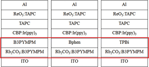
Figure 9. Device performances of three different iOLEDs with the n-B3PYMPM/B3PYMPM homo-junction, n-B3PYMPM/Bphen hetero-junction, and n-B3PYMPM/TPBi hetero-junction as the ETL, respectively. (a) J–V–L and (b) η-L characteristics of the iOLEDs.
5. Organic p–n junction as an efficient electron injection layer
Organic p–n junctions show somewhat different characteristics from crystalline inorganic p–n junctions. One of the most important characteristics of the inorganic p–n junctions is rectification. Using the rectifying property, the current flows are controlled by the direction of the voltage bias. This is actually a core technology in the semiconductor industry. Organic p–n junctions, however, show poor rectifying characteristics and have a high current under reverse bias. Under the reverse bias condition, charges are generated at the junction interface and are transported via tunneling through the narrow depletion layer for several nanometers Citation73 Citation93 Citation94. In the bulk region, the electrons and holes are moved to the electrode by a hopping mechanism because amorphous organic layers have an energetic disorder due to their strongly localized states and polarization, leading to the density of states with Gaussian distribution instead of the band-like structure in the inorganic semiconductors Citation95–98. This interesting behavior of the organic p–n junctions has led them to be frequently utilized as a charge generation layer and a recombination layer in the tandem OLEDs and OPVs, respectively Citation73 Citation98 Citation99,Citation99–115.
Recently, Lee et al. Citation116 successfully adopted the organic p–n junction for the EIL to fabricate a pn-i-p structure. The organic p–n junction consisted of a p-doped copper phthalocyanine (CuPc)/n-doped Bphen layer. As shown in , the forward bias in the iOLEDs corresponds to the reverse bias in the p–n junction. The voltage loss for generating electrons and holes was diminished, and the p–n junction showed very efficient electron and hole generation under a reverse bias, reaching 100 mA/cm2 at 0.3 V. This resulted in the symmetric J–V characteristics under the forward and reverse bias region.
Figure 10. Device structure of the iOLED using the organic p–n junction as an electron injection and electron-transporting layer, and J–V characteristics of the organic p–n junction composed of p-CuPc/n-Bphen. [Reprinted from Lee et al. Citation116, © 2012, with permission from Elsevier.]
![Figure 10. Device structure of the iOLED using the organic p–n junction as an electron injection and electron-transporting layer, and J–V characteristics of the organic p–n junction composed of p-CuPc/n-Bphen. [Reprinted from Lee et al. Citation116, © 2012, with permission from Elsevier.]](/cms/asset/7a86847a-90c2-4ce0-975e-f78775ba2a4c/tjid_a_779324_o_f0010g.jpg)
A remarkable advantage of the new structure using the organic p–n junction is that electrons can be injected and supplied to an emission layer independently of the work function of the bottom cathode. This was experimentally confirmed by using iOLEDs with three different cathodes: poly(3,4-ethylenedioxythiophene)–polystyrenesulfonic acid, UV-O3 treated ITO, and non-treated ITO electrodes with different work functions, respectively. The results are shown in . Interestingly, the iOLEDs with organic p–n junctions were found to have the same J–V–L characteristics independently of the work function of the bottom cathodes, in contrast to the other devices.
Figure 11. Device performances of five different iOLEDs depending on the work function of the bottom cathode. (a) J–V and (b) current density–luminance (L−V) characteristics of the iOLEDs, and the value of the work function of the bottom cathode therein. [Reprinted from Lee et al. Citation116, © 2012, with permission from Elsevier.]
![Figure 11. Device performances of five different iOLEDs depending on the work function of the bottom cathode. (a) J–V and (b) current density–luminance (L−V) characteristics of the iOLEDs, and the value of the work function of the bottom cathode therein. [Reprinted from Lee et al. Citation116, © 2012, with permission from Elsevier.]](/cms/asset/04731efc-b960-43d0-a060-ee6ea8227c61/tjid_a_779324_o_f0011g.jpg)
6. Conclusions
OLEDs have been very successfully applied in small displays and are now moving toward application in large and flexible displays. Low-processing-temperature polysilicone is now in use for fabricating active-matrix circuits in small OLEDs. Oxide semiconductors, however, are good candidates for large TFTs or flexible OLEDs because of their low processing temperature, flexibility, transparency in visible light, and uniformity. As oxide semiconductors are n-type in nature, iOLEDs, where electrons are injected from the bottom electrode, will be more beneficial than normal OLEDs, where holes are injected from the bottom electrode. Unfortunately, however, the efficiency of iOLEDs has not been as good as that of the conventional OLEDs up to recent years, mostly due to the difficulties of electron injection from the ITO or stable metals such as Ag and Al. In this paper, therefore, electron injection and transport are discussed to describe in detail how to enhance the efficiency of iOLEDs. Various methods of enhancing the electron injection from the bottom cathodes to the organic layers are reviewed, especially focusing on the n-doping technology. The importance of the n-ETL/undoped ETL homo- and hetero-junction to realize efficient iOLEDs is also explained. Finally, the p–n junction was introduced as a new kind of EIL that injects electrons very well, independently of the cathode materials.
Acknowledgements
This work was supported by the Industrial Strategic Technology Development Program [10035225, Development of a Core Technology for a High-Performance AMOLED on Plastic] funded by MKE/KEIT.
Related Research Data
References
- Wu , C.-C. , Chen , C.-W. , Lin , C.-L. and Yang , C.-J. 2005 . J. Disp. Technol. , 1 : 248 – 266 . (doi:10.1109/JDT.2005.858942)
- Kho , S. , Sohn , S. and Jung , D. 2003 . Jpn. J. Appl. Phys. , 42 : L552 – L555 . (doi:10.1143/JJAP.42.L552)
- Dobbertin , T. , Kroeger , M. , Heithecker , D. , Schneider , D. , Metzdorf , D. , Neuner , H. , Becker , E. , Johannes , H.-H. and Kowalsky , W. 2003 . Appl. Phys. Lett. , 82 : 284 – 286 . (doi:10.1063/1.1535743)
- Chen , C.-W. , Lin , C.-L. and Wu , C.-C. 2004 . Appl. Phys. Lett. , 85 : 2469 – 2471 . (doi:10.1063/1.1798392)
- Hou , L. , Huang , F. , Zeng , W. , Peng , J. and Cao , Y. 2005 . Appl. Phys. Lett. , 87 : 153509-153509-3
- Chu , T.-Y. , Chen , J.-F. , Chen , S.-Y. , Chen , C.-J. and Chen , C. H. 2006 . Appl. Phys. Lett. , 89 : 053503-053503-3
- Chu , T.-Y. , Chen , S.-Y. , Chen , J.-F. and Chen , C. H. 2006 . Jpn. J. Appl. Phys. , 45 : 4948 – 4950 . (doi:10.1143/JJAP.45.4948)
- Lee , Y. , Kim , J. , Kwon , S. , Min , C.-K. , Yi , Y. , Kim , J. W. , Koo , B. and Hong , M. 2008 . Org. Electron. , 9 : 407 – 412 . (doi:10.1016/j.orgel.2008.01.001)
- Xiong , T. and Ma , D. 2008 . J. Appl. Phys. , 104 : 064506-064506-3
- Zhong , C. , Liu , S. , Huang , F. , Wu , H. and Cao , Y. 2011 . Chem. Mater. , 23 : 4870 – 4876 . (doi:10.1021/cm2025685)
- Zhou , Y. , Fuentes-Hernandez , C. , Shim , J. , Meyer , J. , Giordano , A. J. , Li , H. , Winget , P. , Papadopoulos , T. , Cheun , H. , Kim , J. , Fenoll , M. , Dindar , A. , Haske , W. , Najafabadi , E. , Khan , T. M. , Sojoudi , H. , Barlow , S. , Graham , S. , Brédas , J.-L. , Marder , S. R. , Kahn , A. and Kippelen , B. 2012 . Science , 336 : 327 – 332 . (doi:10.1126/science.1218829)
- Choi , H. W. , Kim , S. Y. , Kim , W.-K. and Lee , J.-L. 2005 . Appl. Phys. Lett. , 87 : 082102-082102-3
- Choi , H. W. , Kim , S. Y. , Kim , W.-K. , Hong , K. and Lee , J.-L. 2006 . J. Appl. Phys. , 100 : 064106-064106-6
- Wang , Q. , Deng , Z. and Ma , D. 2009 . Opt. Express , 17 : 17269 – 17278 . (doi:10.1364/OE.17.017269)
- Bolink , H. J. , Coronado , E. , Orozco , J. and Sessolo , M. 2009 . Adv. Mater. , 21 : 79 – 82 . (doi:10.1002/adma.200802155)
- Yun , C. , Cho , H. , Kang , H. , Lee , Y. M. , Park , Y. and Yoo , S. 2009 . Appl. Phys. Lett. , 95 : 053301-053301-3
- Lee , H. , Park , I. , Kwak , J. , Yoon , D. Y. and Lee , C. 2010 . Appl. Phys. Lett. , 96 : 153306-153306-3
- Yun , C. , Cho , H. , Koh , T.-W. , Kim , J.-H. , Kim , J. W. , Park , Y. and Yoo , S. 2012 . IEEE. Trans. Electron. Dev. , 59 : 159 – 166 . (doi:10.1109/TED.2011.2171488)
- Lee , J.-H. , Lee , S. , Kim , J.-B. , Jang , J. and Kim , J.-J. 2012 . J. Mater. Chem. , 22 : 15262 – 15266 . (doi:10.1039/c2jm32438e)
- Zhou , X. , Pfeiffer , M. , Huang , J. S. , Blochwitz-Nimoth , J. , Qin , D. S. , Werner , A. , Drechsel , J. , Maennig , B. and Leo , K. 2002 . Appl. Phys. Lett. , 81 : 922 – 924 . (doi:10.1063/1.1496502)
- Pfeiffer , M. , Forrest , S. R. , Zhou , X. and Leo , K. 2003 . Org. Electron. , 4 : 21 – 26 . (doi:10.1016/S1566-1199(03)00004-1)
- Zhou , X. , Blochwitz-Nimoth , J. , Pfeiffer , M. , Maennig , B. , Drechsel , J. , Werner , A. and Leo , K. 2003 . Synth. Met. , 138 : 193 – 196 . (doi:10.1016/S0379-6779(02)01265-1)
- Chen , S.-Y. , Chu , T.-Y. , Chen , J.-F. , Su , C.-Y. and Chen , C. H. 2006 . Appl. Phys. Lett. , 89 : 053518-053518-3
- Chu , T.-Y. , Chen , J.-F. , Chen , S.-Y. and Chen , C. H. 2006 . Appl. Phys. Lett. , 89 : 113502-113502-3
- Xiong , T. , Wang , F. , Qiao , X. and Ma , D. 2008 . Appl. Phys. Lett. , 92 : 263305-263305-3
- Wang , F. , Xiong , T. , Qiao , X. and Ma , D. 2009 . Org. Electron. , 10 : 266 – 274 . (doi:10.1016/j.orgel.2008.11.018)
- Lee , J.-H. , Wang , P.-S. , Park , H.-D. , Wu , C.-I. and Kim , J.-J. 2011 . Org. Electron. , 12 : 1763 – 1767 . (doi:10.1016/j.orgel.2011.07.015)
- Thomschke , M. , Hofmann , S. , Olthof , S. , Anderson , M. , Kleemann , H. , Schober , M. , Lüssem , B. and Leo , K. 2011 . Appl. Phys. Lett. , 98 : 083304-083304-3 (doi:10.1063/1.3559847)
- Pope , M. , Magnante , P. and Kallmann , H. P. 1963 . J. Chem. Phys. , 38 : 2042 – 2043 . (doi:10.1063/1.1733929)
- Baigent , D. R. , Marks , R. N. , Greenham , N. C. , Friend , R. H. , Moratti , S. C. and Holmes , A. B. 1994 . Appl. Phys. Lett. , 65 : 2636 – 2638 . (doi:10.1063/1.112587)
- Sato , Y. , Ichinosawa , S. and Kanai , H. 1996 . Inorganic and Organic Electroluminescence , Edited by: Mauch , R. H. and Gumlich , H.-E. Berlin : Wissenschaft und Technik .
- Parker , I. D. 1994 . J. Appl. Phys. , 75 : 1656 – 1666 . (doi:10.1063/1.356350)
- Stössel , M. , Staudigel , J. , Steuber , F. , Simmerer , J. and Winnacker , A. 1999 . Appl. Phys. A: Mater. Sci. Process. , 68 : 387 – 390 . (doi:10.1007/s003390050910)
- Haskal , E. I. , Curioni , A. , Seidler , P. F. and Andreoni , W. 1997 . Appl. Phys. Lett. , 71 : 1151 – 1153 . (doi:10.1063/1.119850)
- Murayama , R. , Kawami , S. , Wakimoto , T. , Sato , H. , Nakada , H. , Namiki , T. , Imai , K. and Nomura , N. Extended Abstracts (The 54th Autumn Meeting 1993) . The Japan Society of Applied Physics , Vol. 3 , pp. 1127
- Kido , J. and Matsumoto , T. 1998 . Appl. Phys. Lett. , 73 : 2866 – 2868 . (doi:10.1063/1.122612)
- Oyamada , T. , Sasabe , H. , Adachi , C. , Murase , S. , Tominaga , T. and Maeda , C. 2005 . Appl. Phys. Lett. , 86 : 033503-033503-3
- Kim , Y.-E. , Park , H. and Kim , J.-J. 1996 . Appl. Phys. Lett. , 69 : 599 – 601 . (doi:10.1063/1.117919)
- Hung , L. S. , Tang , C. W. and Mason , M. G. 1997 . Appl. Phys. Lett. , 70 : 152 – 154 . (doi:10.1063/1.118344)
- Wakimoto , T. , Fukuda , Y. , Nagayama , K. , Yokoi , A. , Nakada , H. and Tsuchida , M. 1997 . IEEE. Trans. Electron. Dev. , 44 : 1245 – 1248 . (doi:10.1109/16.605462)
- Cao , Y. , Yu , G. , Parker , I. D. and Heeger , A. J. 2000 . J. Appl. Phys. , 88 ( 6 ) : 3618 – 3623 . (doi:10.1063/1.1289518)
- Fujikawa , H. , Mori , T. , Noda , K. , Ishii , M. , Tokito , S. and Taga , Y. 2000 . J. Lumin. , 87–89 : 1177 – 1179 . (doi:10.1016/S0022-2313(99)00587-6)
- Ganzorig , C. , Suga , K. and Fujihira , M. 2001 . Mater. Sci. Eng., B , 85 : 140 – 143 . (doi:10.1016/S0921-5107(01)00547-5)
- Heil , H. , Steiger , J. , Karg , S. , Gastel , M. , Ortner , H. , von Seggern , H. and Stößel , M. 2001 . J. Appl. Phys. , 89 : 420 – 424 . (doi:10.1063/1.1331651)
- Xie , Z. T. , Zhang , W. H. , Ding , B. F. , Gao , X. D. , You , Y. T. , Sun , Z. Y. , Ding , X. M. and Hou , X. Y. 2009 . Appl. Phys. Lett. , 94 : 063302-063302-3
- Najafabadi , E. , Knauer , K. A. , Haske , W. , Fuentes-Hernandez , C. and Kippelen , B. 2012 . Appl. Phys. Lett. , 101 : 023304-023304-4 (doi:10.1063/1.4736573)
- Kho , S. , Sohn , S. , Jung , D. , Chae , H. , Boo , J. and Kim , B. 2005 . J. Korean Phys. Soc. , 46 : 1224 – 1227 .
- Khodabakhsh , S. , Poplavskyy , D. , Heutz , S. , Nelson , J. , Bradley , D. D.C. , Murata , H. and Jones , T. S. 2004 . Adv. Funct. Mater. , 14 : 1205 – 1210 . (doi:10.1002/adfm.200400035)
- Lee , J.-H. , Leem , D.-S. , Kim , H.-J. and Kim , J.-J. 2009 . Appl. Phys. Lett. , 94 : 123306-123306-3
- Lee , J.-H. , Leem , D.-S. and Kim , J.-J. 2010 . Org. Electron. , 11 : 486 – 489 . (doi:10.1016/j.orgel.2009.12.002)
- Lee , J.-H. , Kim , H.-M. , Kim , K.-B. and Kim , J.-J. 2011 . Org. Electron. , 12 : 950 – 954 . (doi:10.1016/j.orgel.2011.03.008)
- Lee , J.-H. , Kim , H.-M. , Kim , K.-B. , Kabe , R. , Anzenbacher , P. Jr. and Kim , J.-J. 2011 . Appl. Phys. Lett. , 98 : 173303-173303-3
- Ishii , H. and Seki , K. 1997 . IEEE Trans. Electron. Dev. , 44 : 1295 – 1301 . (doi:10.1109/16.605471)
- Hill , I. G. , Rajagopal , A. and Kahn , A. 1998 . J. Appl. Phys. , 84 : 3236 – 3241 . (doi:10.1063/1.368477)
- Rajagopal , A. and Kahn , A. 1998 . J. Appl. Phys. , 84 : 355 – 358 . (doi:10.1063/1.368035)
- Rajagopal , A. , Wu , C.-I. and Kahn , A. 1998 . J. Appl. Phys. , 83 : 2649 – 2655 . (doi:10.1063/1.367027)
- Blochwitz , J. , Fritz , T. , Pfeiffer , M. , Leo , K. , Alloway , D. , Lee , P. and Armstrong , N. 2001 . Org. Electron. , 2 : 97 – 104 . (doi:10.1016/S1566-1199(01)00016-7)
- Gao , W. Y. and Kahn , A. 2001 . Appl. Phys. Lett. , 79 : 4040 – 4042 . (doi:10.1063/1.1424067)
- Parthasarathy , G. , Shen , C. , Kahn , A. and Forrest , S. R. 2001 . J. Appl. Phys. , 89 : 4986 – 4992 . (doi:10.1063/1.1359161)
- Salaneck , W. R. , Lögdlund , M. , Fahlman , M. , Greczynski , G. and Kugler , T. 2001 . Mater. Sci. Eng. , 34 : 121 – 146 . (doi:10.1016/S0927-796X(01)00036-5)
- Shen , C. and Kahn , A. 2001 . J. Appl. Phys. , 90 : 4549 – 4554 . (doi:10.1063/1.1406967)
- Yan , L. , Watkins , N. J. , Zorba , S. , Gao , Y. L. and Tang , C. W. 2001 . Appl. Phys. Lett. , 79 : 4148 – 4150 . (doi:10.1063/1.1426260)
- Schwieger , T. , Peisert , H. , Golden , M. S. , Knupfer , M. and Fink , J. 2002 . Phys. Rev. B , 66 : 155207-155207-5 (doi:10.1103/PhysRevB.66.155207)
- Gao , W. and Kahn , A. 2003 . Appl. Phys. Lett. , 82 : 4815 – 4817 . (doi:10.1063/1.1585123)
- Gao , Y. and Yan , L. 2003 . Chem. Phys. Lett. , 380 : 451 – 455 . (doi:10.1016/j.cplett.2003.09.012)
- Wu , C.-I. , Lin , C.-T. , Chen , Y.-H. , Chen , M.-H. , Lu , Y.-J. and Wu , C.-C. 2006 . Appl. Phys. Lett. , 88 : 152104-152104-3
- Braun , S. , Salaneck , W. R. and Fahlman , M. 2009 . Adv. Mater. , 21 : 1450 – 1472 . (doi:10.1002/adma.200802893)
- Pfeiffer , M. , Leo , K. and Karl , N. 1996 . J. Appl. Phys. , 80 : 6880 – 6883 . (doi:10.1063/1.363757)
- Harima , Y. , Yamashita , K. , Ishii , H. and Seki , K. 2000 . Thin Solid Films , 366 : 237 – 248 . (doi:10.1016/S0040-6090(00)00887-7)
- Nuesch , F. , Carrara , M. , Schaer , M. , Romero , D. and Zuppiroli , L. 2001 . Chem. Phys. Lett. , 347 : 311 – 317 . (doi:10.1016/S0009-2614(01)01067-3)
- Hayashi , N. , Ishii , H. , Ouchi , Y. and Seki , K. 2002 . J. Appl. Phys. , 92 : 3784 – 3793 . (doi:10.1063/1.1504495)
- Ishii , H. , Hayashi , N. , Ito , E. , Washizu , Y. , Sugi , K. , Kimura , Y. , Niwano , M. , Ouchi , Y. and Seki , K. 2004 . Phys. Status Solidi A , 201 : 1075 – 1094 . (doi:10.1002/pssa.200404346)
- Kröger , M. , Hamwi , S. , Meyer , J. , Dobbertin , T. , Riedl , T. , Kowalsky , W. and Johannes , H.-H. 2007 . Phys. Rev. B , 75 : 235321-235321-8
- Lee , S. , Lee , J.-H. and Kim , J.-J. 2012 . Adv. Funct. Mater. , 22 : 855 – 860 . (doi:10.1002/adfm.201102212)
- Lee , S. , Lee , J.-H. , Kim , K.-H. , Yoo , S.-J. , Kim , T. G. , Kim , J. W. and Kim , J.-J. 2012 . Org. Electron. , 13 : 2346 – 2351 . (doi:10.1016/j.orgel.2012.06.039)
- Yanagi , H. and Okamoto , S. 1997 . Appl. Phys. Lett. , 71 : 2563 – 2565 . (doi:10.1063/1.119331)
- Sirringhaus , H. , Brown , P. J. , Friend , R. H. , Nielsen , M. M. , Bechgaard , K. , Langeveld-Voss , B. M.W. , Spiering , A. J.H. , Janssen , R. A.J. , Meijer , E. W. , Herwig , P. and de Leeuw , D. M. 1999 . Nature , 401 : 685 – 688 . (doi:10.1038/44359)
- Schroeder , P. G. , France , C. B. , Park , J. B. and Parkinson , B. A. 2002 . J. Appl. Phys. , 91 : 3010 – 3014 . (doi:10.1063/1.1445286)
- Kera , S. , Yabuuchi , Y. , Yamane , H. , Setoyama , H. , Okudaira , K. K. , Kahn , A. and Ueno , N. 2004 . Phys. Rev. B. , 70 : 085304-085304-6 (doi:10.1103/PhysRevB.70.085304)
- Koch , N. , Salzmann , I. , Johnson , R. , Pflaum , J. , Friedlein , R. and Rabe , J. 2006 . Org. Electron. , 7 : 537 – 545 . (doi:10.1016/j.orgel.2006.07.010)
- Chen , W. , Huang , H. , Chen , S. , Huang , Y. L. , Gao , X. Y. and Wee , A. T.S. 2008 . Chem. Mater. , 20 : 7017 – 7021 . (doi:10.1021/cm8016352)
- Duhm , S. , Heimel , G. , Salzmann , I. , Glowatzki , H. , Johnson , R. L. , Vollmer , A. , Rabe , J. P. and Koch , N. 2008 . Nat. Mater. , 7 : 326 – 332 . (doi:10.1038/nmat2119)
- Cheng , C. H. , Wang , J. , Du , G. T. , Shi , S. H. , Du , Z. J. , Fan , Z. Q. , Bian , J. M. and Wang , M. S. 2010 . Appl. Phys. Lett. , 97 : 083305-083305-3
- Chen , W. , Qi , D. C. , Huang , H. , Gao , X. Y. and Wee , A. T.S. 2011 . Adv. Funct. Mater. , 21 : 410 – 424 . (doi:10.1002/adfm.201000902)
- Mao , H. Y. , Bussolotti , F. , Qi , D. C. , Wang , R. , Kera , S. , Ueno , N. , Wee , A. T.S. and Chen , W. 2011 . Org. Electron. , 12 : 534 – 540 . (doi:10.1016/j.orgel.2011.01.003)
- Kim , J. W. , Kim , H. J. , Kim , T.-M. , Kim , T. G. , Lee , J.-H. and Kim , J.-J. 2013 . Curr. Appl. Phys. , 13 : 7 – 11 . (doi:10.1016/j.cap.2012.06.003)
- Meier , C. , Ziener , U. , Landfester , K. and Weihrich , P. 2005 . J. Phys. Chem. B. , 109 : 21015 – 21027 . (doi:10.1021/jp054271d)
- Ziener , U. 2008 . J. Phys. Chem. B , 112 : 14698 – 14717 . (doi:10.1021/jp805846d)
- Sasabe , H. and Kido , J. 2011 . Chem. Mater. , 23 : 621 – 630 . (doi:10.1021/cm1024052)
- Yokoyama , D. , Sasabe , H. , Furukawa , Y. , Adachi , C. and Kido , J. 2011 . Adv. Funct. Mater. , 21 : 1375 – 1382 . (doi:10.1002/adfm.201001919)
- Ichikawa , M. , Kawaguchi , T. , Kobayashi , K. , Miki , T. , Furukawa , K. , Koyama , T. and Taniguchi , Y. 2006 . J. Mater. Chem. , 16 : 221 – 225 . (doi:10.1039/b510720b)
- Yokoyama , D. , Sakaguchi , A. , Suzuki , M. and Adachi , C. 2009 . Appl. Phys. Lett. , 95 : 243303-243303-3
- Hamwi , S. , Meyer , J. , Kröger , M. , Winkler , T. , Witte , M. , Riedl , T. , Kahn , A. and Kowalsky , W. 2010 . Adv. Funct. Mater. , 20 : 1762 – 1766 . (doi:10.1002/adfm.201000301)
- Kleemann , H. , Gutierrez , R. , Lindner , F. , Avdoshenko , S. , Manrique , P. D. , Lüssem , B. , Cuniberti , G. and Leo , K. 2010 . Nano. Lett. , 10 : 4929 – 4934 . (doi:10.1021/nl102916n)
- Bässler , H. 1993 . Phys. Status Solidi B , 175 : 15 – 56 . (doi:10.1002/pssb.2221750102)
- Arkhipov , V. I. , Heremans , P. , Emelianova , E. V. and Bässler , H. 2005 . Phys. Rev. B , 71 : 045214-045214-7 (doi:10.1103/PhysRevB.71.045214)
- Coehoorn , R. , Pasveer , W. F. , Bobbert , P. A. and Michels , M. A.J. 2005 . Phys. Rev. B , 72 : 155206-155206-20 (doi:10.1103/PhysRevB.72.155206)
- Richards , T. , Bird , M. and Sirringhaus , H. 2008 . J. Chem. Phys. , 128 : 234905-234905-5 (doi:10.1063/1.2937729)
- Hiramoto , M. , Suezaki , M. and Yokoyama , M. 1990 . Chem. Lett. , 19 : 327 – 330 . (doi:10.1246/cl.1990.327)
- Hiramoto , M. , Fujiwara , H. and Yokoyama , M. 1992 . J. Appl. Phys. , 72 : 3781 – 3787 . (doi:10.1063/1.352274)
- Liao , L. S. , Klubek , K. P. and Tang , C. W. 2004 . Appl. Phys. Lett. , 84 : 167 – 169 . (doi:10.1063/1.1638624)
- Maennig , B. , Drechsel , J. , Gebeyehu , D. , Simon , P. , Kozlowski , F. , Werner , A. , Li , F. , Grundmann , S. , Sonntag , S. , Koch , M. , Leo , K. , Pfeiffer , M. , Hoppe , H. , Meissner , D. , Sariciftci , N. S. , Riedel , I. , Dyakonov , V. and Parisi , J. 2004 . Appl. Phys. A , 79 : 1 – 14 . (doi:10.1007/s00339-003-2494-9)
- Xue , J. G. , Uchida , S. , Rand , B. P. and Forrest , S. R. 2004 . Appl. Phys. Lett. , 85 : 5757 – 5759 . (doi:10.1063/1.1829776)
- Terai , M. , Fujita , K. and Tsutsui , T. 2005 . Jpn. J. Appl. Phys. , 44 : L1059 – L1062 . (doi:10.1143/JJAP.44.L1059)
- Kanno , H. , Holmes , R. J. , Sun , Y. , Kena-Cohen , S. and Forrest , S. R. 2006 . Adv. Mater. , 18 : 339 – 342 . (doi:10.1002/adma.200501915)
- Chan , M.-Y. , Lai , S.-L. , Lau , K.-M. , Fung , M.-K. , Lee , C.-S. and Lee , S.-T. 2007 . Adv. Funct. Mater. , 17 : 2509 – 2514 . (doi:10.1002/adfm.200600642)
- Ho , M.-H. , Hsu , S.-F. , Ma , J.-W. , Hwang , S.-W. , Yeh , P.-C. and Chen , C. H. 2007 . Appl. Phys. Lett. , 91 : 113518-113518-3
- Lai , S. L. , Chan , M. Y. , Fung , M. K. , Lee , C. S. and Lee , S. T. 2007 . J. Appl. Phys. , 101 : 014509-014509-4
- Harada , K. , Riede , M. , Leo , K. , Hild , O. and Elliott , C. 2008 . Phys. Rev. B , 77 : 195212-195212-9
- Leem , D.-S. , Lee , J.-H. , Kim , J.-J. and Kang , J.-W. 2008 . Appl. Phys. Lett. , 93 : 103304-103304-3 (doi:10.1063/1.2979706)
- Liao , L. S. and Klubek , K. P. 2008 . Appl. Phys. Lett. , 92 : 223311-223311-3
- Qi , X. , Li , N. and Forrest , S. R. 2010 . J. Appl. Phys. , 107 : 014514-014514-8 (doi:10.1063/1.3275050)
- Timmreck , R. , Olthof , S. , Leo , K. and Riede , M. K. 2010 . J. Appl. Phys. , 108 : 033108-033108-6 (doi:10.1063/1.3467786)
- Riede , M. , Uhrich , C. , Widmer , J. , Timmreck , R. , Wynands , D. , Schwartz , G. , Gnehr , W. M. , Hildebrandt , D. , Weiss , A. , Hwang , J. , Sundarraj , S. , Erk , P. , Pfeiffer , M. and Leo , K. 2011 . Adv. Funct. Mater. , 21 : 3019 – 3028 . (doi:10.1002/adfm.201002760)
- Li , J. , Bao , Q.-Y. , Wei , H.-X. , Xu , Z.-Q. , Yang , J.-P. , Li , Y.-Q. , Lee , S.-T. and Tang , J.-X. 2012 . J. Mater. Chem. , 22 : 6285 – 6290 . (doi:10.1039/c2jm30272a)
- Lee , J.-H. , Kim , J. W. , Kim , S.-Y. , Yoo , S.-J. , Lee , J.-H. and Kim , J.-J. 2012 . Org. Electon. , 13 : 545 – 549 . (doi:10.1016/j.orgel.2011.12.024)