Abstract
In the former experiment, the effect of aging temperature on the discharge characteristics of the magnesium oxide (MgO) film of the alternating-current plasma display panel was investigated from the point of view of surface contamination. It was found that C and H surface contamination can affect the surface properties, such as the surface conductivity and secondary electron emission (SEE) yield, of the MgO surface. For a better understanding of the effect of C and H contamination on the MgO surface properties, the electronic structures of C- and H-adsorbed MgO (100) surfaces were calculated through the first-principles method, using Cambridge Serial Total Energy Package. The occupied defect levels of the C-adsorbed MgO (100) surface, which lie in the mid-gap, play an important role in the potential emission mechanism of SEE. More C contamination at the MgO surface can induce more SEE and can thus reduce the firing voltage for discharge. The Fermi level of the H-adsorbed MgO (100) surface cuts the bottom edge of the conduction band, which means that the H-adsorbed MgO (100) surface reveals n-type conductivity. More H contamination at the MgO surface can reduce the wall charge accumulation ability and can thus increase the sustain voltage for discharge.
1. Introduction
Magnesium oxide (MgO) film is widely used as a transparent protective layer in the alternating-current plasma display panel (AC-PDP). The MgO protective layer plays an important role in preventing the dielectric layer from being sputtered by ions. Moreover, the MgO film has a high secondary electron emission (SEE) yield, which reduces the firing voltage Vf for discharge. Another important factor that must be considered in improving the discharge characteristics of AC-PDP is the wall charge accumulation ability at the MgO surface. The high electric resistance of the MgO film reduces the sustain voltage Vs, which is the minimum voltage for maintaining the discharge. Therefore, the discharge characteristics of AC-PDP are critically dependent on the physical and chemical properties of the MgO surface, such as the surface orientation, morphology, defects, and impurities Citation1–3.
In a past experiment Citation4, the effect of aging temperature on the discharge characteristics of the MgO film was investigated from the point of view of the surface contaminations at the MgO surface. In situ characterization of the MgO surface after discharge aging was performed through X-ray photoelectron spectroscopy (XPS) to identify the contaminations at the MgO surface. Discharge aging is usually performed to obtain uniform discharge and to ensure the stable operation of AC-PDP. Silver electrodes were formed on the glass of the front panel using film technology and photolithography. Then, the electric condenser was coated in printing type. After forming the sealing material, a 500-nm-thick MgO film was deposited through the electron beam evaporation technique on the dielectric layer. The prepared samples were subjected to thermal annealing in an aging chamber for 30 min, at 350°C, to activate the MgO surface. The base pressure of the aging chamber was 5×10⁻⁷ Torr. After annealing, the main process of 6-hour discharge aging was performed at 25, 100, 150, and 200°C. The aging chamber was filled with Ne–Xe (4%) gas at a pressure of 400 Torr. The discharge voltage of the gas mixture was maintained at 210 V. The composition of the plasma near the MgO surface was monitored via optical emission spectroscopy during discharge Citation4. shows the measured firing voltage Vf, sustain voltage Vs, and memory coefficient MC [=2 × (Vf − Vs)/Vf] of the MgO films as a function of the aging temperatures of the substrate. The data for the 200°C substrate temperature were omitted because it was impossible to perform the discharge aging at that temperature. The firing voltage Vf at room temperature was 260 V, whereas the sustain voltage Vs was 180 V, which resulted in the memory coefficient MC value of 0.62. After discharge aging at 100°C, both the Vf and Vs values were reduced compared with the values at room temperature. The value of MC, however, increased, which indicates that the amount of reduction of Vs was bigger than that of Vf. The greater the value of MC is, the higher the probability of the stable operation of AC-PDP. Thus, discharge aging at 100°C substrate temperature yields better discharge characteristic results than that at room temperature does. The value of MC, however, drops sharply at 150°C substrate temperature. This poor memory margin comes from the sharp increase in sustain voltage Vs and a certain decrease in firing voltage Vf. The discharge characteristic results revealed that 100°C aging temperature is preferable to other aging temperatures, such as 25°C and 150°C Citation4. To understand the tendency of the discharge characteristics at various aging temperatures, the variation of the compositional elements at the MgO surface must be studied. The XPS wide-scan spectra with increasing substrate temperatures of (a) 25°C, (b) 100°C, and (c) 150°C are shown in Citation4. In the XPS wide-scan spectra, one can see the Mg 2s, Mg 2p, O 1s, and O Auger peaks originated from the MgO film. Besides the expected peaks of Mg and O, there are C 1s and C Auger peaks in the spectra, which were from the contamination of C at the MgO surface. Xe 3d peaks of around 675 eV can be seen at the spectrum of 25°C aging temperature, while no visible Xe 3d peaks can be seen at 100°C and 150°C. There was no evidence for Ne even in the spectrum of 25°C aging temperature, which was the major component of the gas mixture for discharge. The peak intensity of C 1s was reduced when the aging temperature of the sample increased from 25°C to 100°C. At 150°C aging temperature, however, the peak intensity of C 1s increased to some extent. This kind of tendency is similar to that of the measured value of sustain voltage Vs in . shows the XPS O 1s narrow-scan spectra
Figure 1. Firing voltage Vf, sustain voltage Vs, and memory coefficient MC of the MgO films as a function of the aging temperatures of the substrate Citation4.
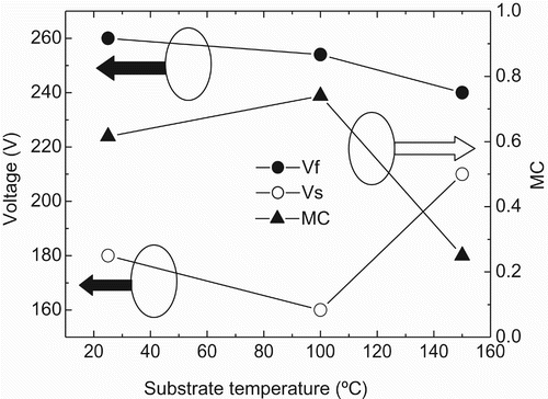
Figure 2. XPS wide-scan spectra of the MgO films at three different aging temperatures: (a) 25°C; (b) 100°C; and (c) 150°C Citation4.
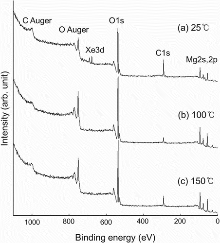
Figure 3. XPS O1s narrow-scan spectra of the MgO films at three different aging temperatures (25°C, 100°C, and 150°C) compared with the pre-aging sample (As-dep) Citation4.
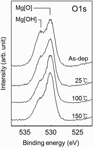
with increasing substrate temperatures of 25°C, 100°C, and 150°C compared with the pre-aging sample (As-dep) Citation4. The intensity of the hydroxyl groups marked as Mg[OH] in decreased significantly at 25°C compared with the pre-aging sample, and reached the minimum value at 100°C. At 150°C, however, the intensity of the hydroxyl groups seemed to have increased again. This kind of intensity variation is similar to that of the C 1s peak intensity in . In ,
it can be seen that sustain voltage Vs has the smallest value at 100°C aging temperature. Firing voltage Vf, however, decreased as the aging temperature increased to 150°C. It can be inferred from the above observation that the C and H surface contamination can affect the surface properties of the MgO film. The surface conductivity of the MgO film is related to sustain voltage Vs, and the SEE yield is related to firing voltage Vf.
In this work, the electronic densities of states (DOS) of the C- and H-adsorbed MgO (100) surfaces were calculated through the first-principles method to obtain a better understanding of the relationships among the surface electronic structures, the surface properties, and the discharge characteristics.
2. Computational setup
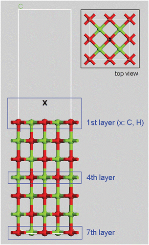
The electronic DOSs of the C- and H-adsorbed MgO (100) surfaces were calculated using Cambridge Serial Total Energy Package (CASTEP) Citation5 Citation6. CASTEP is a first-principles quantum mechanical code for performing electronic-structure calculations. Within the density functional formalism, it can be used to simulate a wide range of materials, including crystalline solids, surfaces, molecules, liquids, and amorphous materials. A graphical user interface from Accelrys, Inc., the Materials Studio 4.2 package, has been used to build the initial structure, to generate input files, to run the calculation, and finally, to analyze the data. It can be easily used to visualize final crystal structures, electronic band structures, and DOSs. The 16-node Linux cluster was used for the parallel calculation of the electronic DOSs of 28 Mg and 28 O atoms with seven layers for the MgO (100) surface, which means 4 Mg and 4 O atoms per layer. shows the supercell structure of Mg28O28 with the contaminant X (C, H) above O. The light-colored (green) ball is Mg, and the dark-colored (red) one is O. The thickness of the vacuum slab was set to 12.9 Å, which is the same as those of the seven atomic layers. The generalized gradient approximation scheme with the Perdew Burke Ernzerhof exchange-correlation functional was chosen for the CASTEP calculation of the geometry optimization task. Pseudo-atomic calculation was performed for the Mg 2p63s2 and O 2s22p4 configurations. Partial DOS (PDOS) was also chosen for the calculation to determine the DOS of each separate layer.
Figure 4. Supercell structure for the MgO (100) surface model with seven atomic layers. The light-colored (green) ball is Mg, and the dark-colored (red) one is O. The thickness of the vacuum slab was set to 12.9 Å (color online).
3. Results and discussion
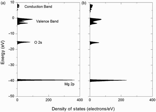
shows a typical result of the electronic DOS for the bulk model of MgO crystal with 32 Mg and 32 O atoms in a cubic supercell without a vacuum slab Citation7. Sharp and featureless peaks of Mg 2p and O 2s can be seen. The Fermi level was set to zero at the top of the valence band (VB). A conduction band (CB) existed above the VB, with the band gap (BG) in between, which was found to be 5.40 eV for the bulk MgO crystal. shows the calculated electronic DOS for the surface model of the clean MgO (100) surface. The supercell structure for the surface model is shown in without C and H contamination. The area beneath the Fermi level was integrated into 392 electrons, which were composed of 28 times 8 electrons of Mg and 6 electrons of O. Due to the surface effect, the shapes of VB and CB had been changed. The value of the BG of the clean MgO (100) surface was found to be 4.21 eV, which is one of the significant changes from the bulk to the surface.
Figure 5. DOSs of the (a) bulk MgO crystal Citation7 and (b) clean MgO (100) surface without contaminations in full scale.
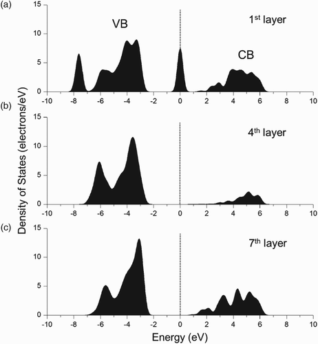
shows the calculated electronic PDOS of the C-adsorbed MgO (100) surface. The displayed energy range is from −10 to 10 eV, and the Fermi level at zero is marked with vertical dashed lines. shows the PDOS of the C-adsorbed first layer, the bulk-like fourth layer, and the clean surface of the seventh layer. The Fermi level, which cuts the defect state of the C-adsorbed MgO (100) surface, is at 3.09 eV above the VB. It can be seen in and that the defect level was in the mid-gap and did not overlap with the CB. Two electrons were occupied in the defect level. The occupied defect levels in the BG play an important role in the potential emission mechanism of SEE induced by low-energy Ne and Xe ions. This process is called Auger neutralization process Citation8 Citation9. Ne ion with greater ionization energy than Xe ion has a greater SEE yield value. The SEE yield also increases with the presence of defect states in the BG of the MgO film. A higher defect level appears to be advantageous for obtaining a larger SEE yield Citation10 Citation11. It was found that occupied defect states such as an oxygen vacancy (F-center) lying in the BG of MgO can cause an increase in the SEE yield Citation12. The occupied defect state of the C-adsorbed MgO (100) surface could also contribute to an increase in the SEE yield in the case reported herein. This means that more C contamination at the MgO surface can induce more SEE and can thus reduce firing voltage Vf for discharge.
Figure 6. PDOS of the C-adsorbed MgO (100) surface: (a) C-adsorbed first layer; (b) bulk-like fourth layer; and (c) clean surface of the seventh layer.
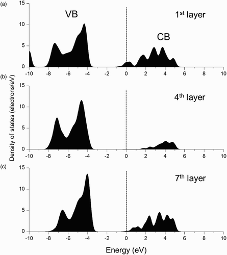
shows the calculated electronic PDOS of the H-adsorbed MgO (100) surface. shows the PDOS of the H-adsorbed first layer, the bulk-like fourth layer, and the clean surface of the seventh layer. The Fermi level, which cuts the defect state of the H-adsorbed MgO (100) surface, is at 4.08 eV, above the VB. It can be seen from the bulk-like PDOS in that the defect level was in the mid-gap. It can be seen from the PDOSs in and , however, that the Fermi level cuts the bottom edge of the CB. This kind of configuration can generate n-type conductivity at the H-adsorbed MgO (100) surface, which reduces the electrical resistivity at the surface. This means that more H contamination at the MgO surface can reduce the wall charge accumulation ability and can thus increase sustain voltage Vs for discharge.
Figure 7. PDOS of the H-adsorbed MgO (100) surface: (a) H-adsorbed first layer; (b) bulk-like fourth layer; and (c) clean surface of the seventh layer.
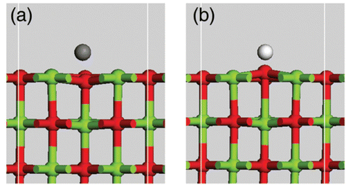
shows the side view of the geometry-optimized atomic structure of the C- and H-adsorbed MgO (100) surfaces. The optimized bond length of C‒O is 1.4 Å in and ‒O 1.0 Å in . C tends to push the oxygen atom into the bulk whereas H tends to extract the oxygen atom from the surface. This means that the strength of the Mg‒O bond around the C-adsorbed MgO site tends to increase, whereas that of the Mg‒O bond around the H-adsorbed MgO site tends to decrease. This indicates that H may generate more oxygen vacancy, namely the F-center at the MgO (100) surface.
Figure 8. Geometry-optimized atomic structure of the (a) C- and (b) H-adsorbed MgO (100) surfaces (color online).
4. Conclusion
The effect of C and H contamination on the MgO surface properties was studied through the first-principles method. The PDOSs of the C- and H-adsorbed MgO (100) surfaces were calculated using CASTEP. The occupied defect levels of the C-adsorbed MgO (100) surface, which lie in the mid-gap, play an important role in the potential emission mechanism of SEE induced by low-energy Ne and Xe ions. The SEE yield increases with the presence of defect states in the BG of the MgO film. More C contamination at the MgO surface can induce more SEE and can thus reduce firing voltage Vf for discharge. The Fermi level of the H-adsorbed MgO (100) surface cuts the bottom edge of the CB, which means that the H-adsorbed MgO (100) surface reveals n-type conductivity. More H contamination at the MgO surface can reduce the wall charge accumulation ability and can thus increase sustain voltage Vs for discharge.
References
- Choi , E. H. , Lim , J. Y. , Kim , Y. G. , Ko , J. J. , Kim , D. I. , Lee , C. W. and Cho , G. S. 1999 . J. Appl. Phys. , 86 : 6525 – 6527 . (doi:10.1063/1.371618)
- Park , C. H. , Kim , Y. K. , Park , B. E. , Lee , W. G. and Cho , J. S. 1999 . Mater. Sci. Eng. B , 60 : 149 – 155 . (doi:10.1016/S0921-5107(99)00028-8)
- Uchiike , H. and Harada , S. 1991 . SID’91 Digest , : 444 – 447 .
- Joo , M. H. , Park , K. H. and Lee , J. W. 2008 . J. Surf. Anal. , 14 : 412 – 415 .
- Segall , M. D. , Lindan , P. J.D. , Probert , M. J. , Pickard , C. J. , Hasnip , P. J. , Clark , S. J. and Payne , M. C. 2002 . J. Phys.: Cond. Matt. , 14 : 2717 – 2743 . (doi:10.1088/0953-8984/14/11/301)
- Clark , S. J. , Segall , M. D. , Pickard , C. J. , Hasnip , P. J. , Probert , M. J. , Refson , K. and Payne , M. C. 2005 . Z. Kristallogr. , 220 : 567 – 570 . (doi:10.1524/zkri.220.5.567.65075)
- Lee , J. W. submitted to J. Korean Phys. Soc. ,
- Hagstrum , H. D. 1954 . Phys. Rev. , 96 : 336 – 365 . (doi:10.1103/PhysRev.96.336)
- Aboelfotoh , M. O. and Lorenzen , J. A. 1977 . J. Appl. Phys. , 48 : 4754 – 4759 . (doi:10.1063/1.323490)
- Yoon , S. J. , Lee , I. , Lee , J. W. and Oh , B. 2001 . Jpn. J. Appl. Phys. , 40 : 809 – 812 . (doi:10.1143/JJAP.40.809)
- Motoyama , Y. , Hirano , Y. , Ishii , K. , Murakami , Y. and Sato , F. 2004 . J. Appl. Phys. , 95 : 8419 – 8424 . (doi:10.1063/1.1751239)
- Cho , Y. , Kim , C. , Ahn , H. S. , Cho , E. , Kim , T. E. and Han , S. 2007 . J. Appl. Phys. , 101 : 0837101 – 8030107 .