Abstract
A new multi-domain driving technology for a vertically placed RGB pixel structure with subpixels (MB7) was developed. Subpixel A (high-tilt-angle domain) was charged with the data voltage, without any change. The two directly connected thin-film-transistors (TFTs) functioning as a parallel-resistors circuit could reduce the data voltage supplied to subpixel B (low-tilt-angle domain). The amount of voltage drop for subpixel B could be easily controlled by adjusting the TFT channel width ratio between the parallel resistors. Through the use of this new method, a 32-in. HD TFT liquid crystal display (TFT-LCD) TV panel with a wide viewing angle was successfully fabricated.
1. Introduction
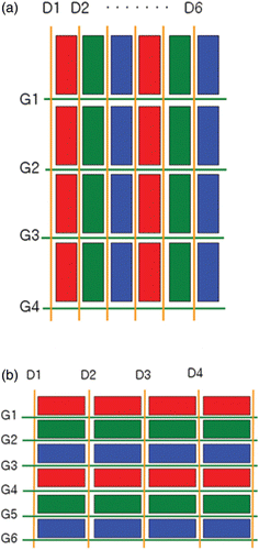
The thin-film-transistor liquid crystal display (TFT-LCD) has a wide range of applications in consumer products such as TVs, notebook PCs, and desktop computer monitors Citation1. One of the most important aspects of TFT-LCD devices is the cost. As D-ICs (driver integrated circuits) greatly contribute to the cost of TFT-LCD panels, various attempts to reduce the number of D-ICs have been made by many companies and academics Citation2 Citation3. Samsung has developed the MB7 technology, in which the RGB pixels are placed vertically so that they share a single data line (). The number of data lines is reduced by a third. The MB7 structure, however, has only four domains, and the gamma curves show discrepancy as the viewing angle changes from the normal direction to an oblique direction.
Figure 1. Diagram of the MB7 structure: (a) conventional array and (b) vertically placed pixel array.
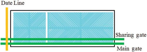
Although various methods for eight-domain driving have been developed, such as the CS type (charge share, Samsung) Citation4, the ART-CC type (additional refresh TFT capacity-coupled, AUO) Citation5, and the TT type (two-TFT and dual-data-line, Samsung) Citation6. These methods may not be adopted to the MB7 structure. The CC type has a serious image sticking due to the floating electrode of the capacitance. Although the ART-CC type can remove the charge stored in the floating electrode, its aperture ratio is smaller than those of the other types, resulting from the additional capacitance. The CS-type driving method needs additional sharing gate lines, resulting in reduced transmittance (). The TT type requires doubling of the number of data lines for charging two different subpixels to increase the cost by adding source D-ICs.
Figure 2. CS type for the MB7 structure.
In this paper, a new eight-domain driving technology that needs neither extra sharing gate lines nor additional data lines for the most cost-effective MB7 device is proposed. The proposed mode, the resistivity division (RD) mode, improves the off-axis performance (color washout) and the panel transmittance compared with the conventionally manufactured MB7 product.
2. Results and discussion
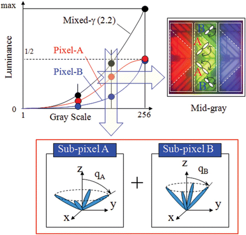
The four-domain vertical alignment (VA) TFT-LCD devices exhibit image quality deterioration depending on the viewing direction. As a result, the skin color becomes whitish as viewed from an oblique direction, termed “color washout”, which is measured by the Gamma Distortion Index (GDI) Citation7.
To efficiently reduce the color washout (or decrease the GDI), a pixel is divided into high-pixel (subpixel A, high-tilt-angle zone) and low-pixel (subpixel B, low-tilt-angle zone), which doubles the number of liquid crystal (LC) domains from four to eight. This concept is illustrated in .
Figure 3. Eight-domain driving for the improvement of the off-axis image quality in the VA mode.
2.1. Theoretical studies of RD
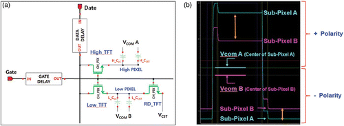
The proposed RD type is similar to the CS type in terms of dividing a pixel into two subpixels and charging each subpixel with different voltages, but its operation principle is totally different from that of the CS type. The pixel circuit and image of RD for MB7 are shown in . shows a schematic representation of the operation principles.
Figure 4. Pixel circuit for the RD type: (a) equivalent circuit and (b) diagram for operation.
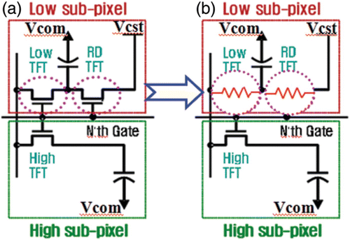
When the Nth gate is turned on, the high subpixel is supplied with data voltage, and the low subpixel is charged with decreased data voltage. The input data voltage is decreased by leakage to the Vcst line through RD-TFT, making the low subpixel darker than the high subpixel. The amount of leakage is determined by the TFT size of the RD. The two directly connected TFTs (low and RD TFTs) functioning as a parallel-resistors circuit can reduce the data voltage supplied to subpixel B ().
2.2. Simulation studies for the optimal design rule
The charging properties of the two subpixels were calculated using the Spice Program (). At positive polarity, the charging voltage difference between subpixel A and subpixel B is bigger than the one at negative polarity. As shown by this result, Vcom A (the common electrode voltage for subpixel A) differs from Vcom B (the Vcom for subpixel B). If Vcom is set to Vcom A, the low pixel will have inappropriate characteristics, especially increased flicker and decreased transmission. For the optimal device properties, Vcom A and Vcom B should match. As shown in , the given data voltage flows to the Vcst (reference voltage for storage capacitance) line. Therefore, Vcom B can be adjusted to Vcom A by controlling the Vcst level.
Figure 5. Simulation schematic and charging properties for the RD type: (a) schematic for simulation and (b) charging properties of the subpixels.
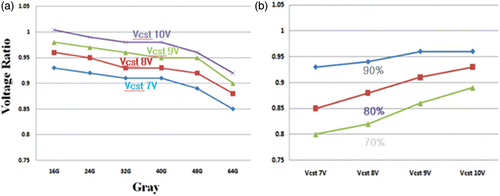
To understand the principles of the RD type according to the change in Vcst, the circuit was designed as shown in . With this circuit, the voltage ratio data, defined as the voltage of subpixel B divided by the input data voltage, were calculated. The voltage ratio results are shown in . The voltage ratio was steadily reduced by increasing the grayscale and the Vcst level, as shown in . Based on these results, the optical characteristics, such as the luminance of subpixel B and the GDI, can be tuned by controlling the Vcst level. In addition to the modulation of Vcst, the voltage ratio was controlled by changing the RD-TFT size (width×length dimensions). In , it is indicated that the increase in the size of the RD TFT points to a decrease in voltage ratio, and that the channel dimension of the RD TFT is inversely proportional to the voltage ratio. The simulation data show that the Vcst level is a crucial factor for adjusting Vcom B to Vcom A. In other words, the performance of a display, such as the flicker and image sticking, can be improved by controlling the Vcst level in the RD type.
Figure 6. Voltage ration simulation results of subpixel B: (a) voltage ratio from gray in the Vcst level and (b) Vcst influence from the RD-TFT size.
2.3. Preparing and measuring the prototype panels
Prototype panels with various parameters were designed and evaluated in the development line to investigate the relationship between the low-subpixel-TFT width and the RD TFT width. The results are summarized in .
Table 1. Prototype evaluation results.
The higher the area ratio between the high and low pixels is, the better the image quality at the off-axis. The lower the voltage ratio between the high and low pixels is, the better the image quality at the off-axis, but the transmittance property is decreased. The transmittance and off-axis image quality have a trade-off relationship. The optimal design rule for mass products can be determined to obtain a high transmittance and a low GDI property (better off-axis image quality). In this research, it was found that the low TFT percentage was positively correlated with the voltage ratio. Generally, the GDI of the eight-domain VA structure is 0.3. The design rule for the optimal RD mode is 1:1.25 area ratio and 80% low TFT.
2.4. 32 in. HD LCD TV and off-axis gamma property comparison
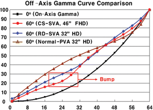
A 32 in. HD RD-type panel was successfully developed at the 8–1 line. shows the improved off-axis gamma of the RD type, much closer to the on-axis 2.2 gamma compared with the normal four-domain-patterned VA (PVA). The off-axis gamma of the CS type has a middle-gray bump, causing a yellowish problem. The removal of the bump in the RD type addressed the yellowish problem.
Figure 7. Off-axis gamma comparison.
The newly developed RD-type eight-domain driving technology can improve the color washout from the normal PVA, and the off-axis image quality is similar to that of the CS type in MB 4 (the conventional RGB array) structure, which is the premium display.
3. Conclusion
The RD-type TFT-LCD TV was developed to effectively reduce the GDI to below 0.3. In addition, the RD type is more cost-effective than the other eight-domain VA mode due to its higher aperture ratio and as it has no need for external electric components such as a source D-IC (driver IC) or a gate line ().
Table 2. Properties comparison among the operation types of the VA mode.
References
- Fujiware , M. 2001 . SID’01 Digest , 32 : 251 (doi:10.1889/1.1831843)
- Sakamoto , M. , Okutani , S. , Koga , K. , Hada , H. and Ohi , S. 1997 . SID’97 Digest , 28 : 387
- Sung , Y.-C. , Choi , B.-D. and Kwon , O.-K. 2002 . SID’02 Digest , 33 : 913 (doi:10.1889/1.1830932)
- Park , S. B. , Lyu , J. , Um , Y. , Do , H. , Ahn , S. , Choi , K. , Kim , K.-H. and Kim , S. S. 2007 . SID’07 Digest , 38 : 1252 (doi:10.1889/1.2785538)
- Huang , Y.-P. , Huang , W.-K. , Tsao , C.-H. , Su , J.-J. , Hou , H.-L. , Liao , L. , Lee , C.-Y. , Chang , T.-R. , Lin , Y.-C. and Chen , P.-L. 2007 . SID’07 Digest , 38 : 1010 (doi:10.1889/1.2785476)
- Kim , S. S. 2005 . SID’05 Digest , 36 : 1842 (doi:10.1889/1.2036378)
- Kim , S. S. 2004 . SID’04 Digest , 35 : 760 (doi:10.1889/1.1825793)