Abstract
This paper analyses the degradation of the optical, electrical, and thermal characteristics of InGaN/GaN-based light-emitting diodes (LEDs) with different chip sizes. Their optical, electrical, and thermal characteristics were periodicity-monitored during the test. The small chip showed an increase in ideality factor and high series resistance. This led to the degradation of the electrical characteristic, and hence to high thermal resistance, finally resulting in low light output power. In the large chip, the high operating current made the junction temperature high. This, together with the thermal degradation on the LED surface and metal pad, led to a decrease in light output power. In the middle chip, the optical and electrical degradation ratio was lower than that in the other samples and, therefore, the light output power decreased to a lesser degree.
Introduction
GaN-based light-emitting diodes (LEDs) provide a number of advantages over the conventional light sources, such as reduced power consumption, high color purity, long lifetime, and low cost, all of which are continuously improving [Citation1–3]. There have been rapid developments in GaN-based LEDs for their application to solid-state lighting and high-performance backlighting units in liquid crystal displays [Citation4–6]. LEDs have a number of faults, however, which have been studied over the last decade. What has been established, however, about the reliability and failure mechanism of InGaN/GaN-based LED is only that the degradation and failure of the commercial packaged GaN-based LED are primarily associated with the package rather than with the GaN-based blue LED chip itself [Citation7–10]. According to these papers, the failure mechanisms that were related to the package were associated with the die attach condition, injection current density, packaging materials, ohmic contact and electrode bonding, and discoloration of the encapsulation materials. In addition, the optical, electrical, and thermal degradation of GaN-based LED are being studied separately [Citation11–14].
In this paper, the relationships among the optical, electrical, and thermal characteristics of GaN-based LEDs, by which the degradation of blue LED chips can be analyzed, are proposed. Three kinds of chips from the same manufacturer were analyzed in this study, using the conventional plastic white package. The optical, electrical, and thermal characteristics of the samples, such as their light output power degradation, ideality factor, series resistance, reverse leakage current, junction temperature, and thermal resistance, were investigated and analyzed.
Experiment
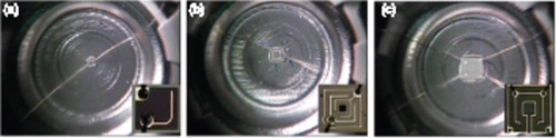
The devices that were used in this study were three InGaN/GaN-based blue LEDs with different sizes provided by the same manufacturer. They were designated as samples A, B, and C and had ,
, and
m chips, respectively, as shown in . As for the structure of the devices, they were composed of InGaN/GaN-based LEDs in standard configuration attached to a copper frame that operates without a heat sink and epoxy resin. The plastic white package was located around the chip and acted like a reflector cup. After the initial characterization, the devices that exhibited stable samples were selected to carry out the degradation tests. The aging time of 100 h was used. The initial characterization consisted of optical, electrical, and thermal measurements. The optical output power was collected with an integral sphere using the OL770 optical measurement system. In addition, I−V characterization was performed with a probe station in the range of 10 to -10 V. Then the results of the I−V characterization were used for the values of the ideality factor and series resistance. For the analysis of the thermal characteristics of these samples, their thermal characteristics were investigated by means of thermal-resistance measurement using a{\newpage} thermal transient tester. In the JEDEC standard, for a single chip package, the relationship between thermal resistance and junction temperature can be explained by the following equation [Citation15]:
Figure 1. Image of (a) sample A, (b) sample B, and (c) sample C. The inset images are the top views of the chips.
Results and discussion
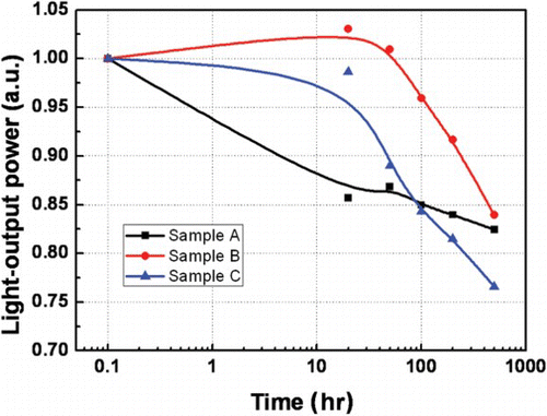
The relative light output power of the GaN-based blue LED chips as a function of the operating time (0–500 h) and chip size is shown in . The figure shows the degradation characteristics of the tested samples A, B, and C with a testing current density of 40 A/cm2 and an ambient temperature of about 80°C. The injection currents of the three samples for the test were 49, 144, and 400 mA, respectively. As shown in , the degradation rates of the light output power to the initial value at 500 h of the three samples were 17.6%, 16.1%, and 23.4%, respectively.
Figure 2. Relative light output power vs. test time characteristics of the samples.
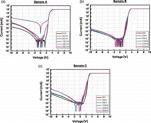
To investigate the relation between the optical degradation and the electrical characteristics [Citation17], the I−V curves of the three samples were measured, as shown in . The figure shows the I−V characteristics of the tested samples as a function of the operating time with a testing current density of 40 A/cm2. Comparing the degradation of the three different types of chips with the same testing current density and the same package, samples B and C showed the highest leakage current stability in the reverse region, as shown in (b) and 3(c). On the other hand, the I−V curve of sample A was over the 1 μA range even after testing at 500 h, as shown in (a). These results show a close correlation between the degradation of the light output power and the degradation of the electrical characteristics.
Figure 3. I−V characteristics of (a) sample A, (b) sample B, and (c) sample C by test time.
The series resistance and ideality factor of the three samples are shown in . The corresponding ideality factors are shown with the dashed line in and were inferred from the measurement using the ideality factor equation [Citation18,Citation19]. All the samples of the ideality factor had its value starting from 3, but after the aging time, it was found to increase dramatically in samples A and C. As can be seen from the I−V characteristic of the degradation of the electrical property, the ideality factor will also have a high value. On the other hand, sample B shows a more stable ideality factor value compared with samples A and C after the test time. This result shows a more stable characterization of the I−V curve compared with samples A and C. The series resistance is shown with the line in and was inferred from the measurement using
Figure 4. Series resistance and ideality factor of (a) sample A, (b) sample B, and (c) sample C by test time.
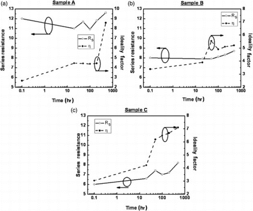
Therefore, the curve of vs. I will have a slope given by the series resistance (
). Sample A had a higher series resistance value than samples B and C. The reason for this was the low current spreading due to the metal pad configuration. As for the low series resistance values of samples B and C, however, which are shown in , it is well considered that the reason for them was the pad configuration. The relation between the optical degradation and the electrical characteristics was investigated [Citation20]. The electrical degradation was found to be related to the optical degradation. The high ideality factor and series resistance values were due to the optical degradation, as shown in . The degradation of the electrical characteristics reduced the e–h pair combination rate of the multiple quantum wells, and the light output power was found to have been reduced as well [Citation21].
For the investigation of the thermal characterizations of the three types of chips, the junction temperature and thermal resistance were measured [Citation22]. (a) shows the junction temperatures of the tested samples as a function of the operating time, with a testing current density of 40 A/cm2. For the measurement of the test current for the junction temperature of the three samples, 20 mA (sample A), 150 mA (sample B), and 200 mA (sample C) were used at 25°C, respectively. The junction temperature of sample A increased from 8.69°C to 13.58°C; that of sample B from 63.16°C to 68.02°C; and that of sample C from \colfigright{}
Figure 5. (a) Junction temperature and (b) thermal resistance of the samples by test time.
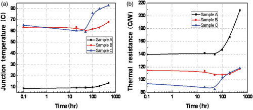
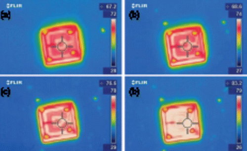
65.18°C to 82.85°C. The junction temperature did not increase much in samples A and B. It increased by approximately 17°C in sample C as a result of the pad configuration of the surface and the increase in the temperature on the LED surface, as can be seen in the FLIR image in . Images from the other samples could not be obtained because precise focus could not be made. (b) shows how the thermal resistance changed over time during the test in each sample. In sample A, the junction temperature did not increase, but the thermal resistance was high because the electrical property was relatively degraded, resulting in input power loss. In sample C, the electrical property changed and became more stable than in sample A and, therefore, the thermal resistance changed in the same pattern as the junction temperature did. In sample B, however, the stable electrical property and low junction temperature led to stable thermal resistance over time. Put in a different way, in sample A, the degradation of the electrical property caused the thermal resistance to increase much and the light output power to relatively decrease, but in sample C, the degradation of the electrical property was more stable and, as such, the thermal resistance did not rise much, although the thermal degradation of the LED surface and metal pad caused the light output power to decrease. On the other hand, sample B showed a stable electrical property and thermal characterization and, as such, the light output power decreased to a lesser degree than in the other samples. Comparing the degradation of the three different types of chips with the same measurement conditions, the thermal degradation was related more to the ideality factor than to the series resistance, as shown in . In other words, the rapid increase in the ideality factor value was related more to the thermal degradation than to the series resistance.
Figure 6. FLIR image of sample C at (a) initial, (b) 100 h, (c) 200 h, and (d) 500 h.
Conclusion
In this paper, the optical, thermal, and electrical characteristics were analyzed using three LEDs with different sizes but applied to the same package. Sample A, m in size, showed an increase in ideality factor and high series resistance. This led to the degradation of its electrical property, and hence, to high thermal resistance, finally resulting in low light output power. In sample C,
m in size, the high operating current made the junction temperature high. This, together with the thermal degradation on the LED surface and metal pad, as verified in the Forward Looking Infrared (FLIR) image, led to a decrease in light output power. In sample B,
m in size, the optical and electrical degradation ratio was lower than that in the other samples, and as such, the light output power decreased to a lesser degree. These results call for further research on ohmic contact and pad configuration to reduce the input power and to improve the properties of smaller chips. Also, research on pad configuration and on a thermal management technique for decreasing the high junction temperature is necessary for larger chips.
Funding
This research was financially supported by the Ministry of Trade, Industry, & Energy (MOTIE), Korea Institute for Advancement of Technology (KIAT), and Honam Institute for Regional Program Evaluation through the Leading Industry Development for Economic Region Program.
References
- E.F. Schubert and N.E.J. Hunt, Appl. Phys. A. 66, 319 (1998). doi: 10.1007/s003390050672
- X.A. Cao and S.D. Arthur, Appl. Phys. Lett. 85, 3971 (2004). doi: 10.1063/1.1810631
- L.-C. Chen and Y.-L. Huang, Solid-state Electron. 48, 1239 (2004). doi: 10.1016/j.sse.2004.02.003
- E.F. Schubert, Light-Emitting Diodes (Cambridge University Press, Cambridge, UK, 2003).
- M. Koike, N. Shibata, H. Kato and Y. Takahashi, IEEE J. Sel. Top. Quantum Electron. 8, 271 (2002). doi: 10.1109/2944.999180
- S.J. Chang, W.C. Lai, Y.K. Su, J.F. Chen, C.H. Liu and U.H. Liaw, IEEE J. Sel. Top. Quantum Electron. 8, 278 (2002). doi: 10.1109/2944.999181
- L. Wang, S. Feng, C. Guo and G. Zhang, presented at the IEEE Proceedings of 16th IPFA, 2009, p. 472.
- L. Yang, J. Hu and M.W. Shin, Solid-State Electron. 53, 567 (2009). doi: 10.1016/j.sse.2009.03.014
- X. Luo, B. Wu and S. Liu, IEEE Trans. Device Mater. Reliab. 10 (2) (2010).
- F. Wu, W. Zhao, S. Yang, and C. Zhang, presented at the Electronic Measurement & Instruments of ICEMI ’09, 2009, p. 4–978.
- M. Meneghini, L.R. Trevisanello, G. Meneghesso and E. Zanoni, IEEE Trans. Device Mater. Reliab. 8 (2) (2008).
- S.-L. Kuo, C.-K. Liu, M.-J. Dai, C.-K. Yu, H.-C. Chien and C.-Y. Hsu, presented at the Electronics Packaging Technology Conference(EPTC) 2008. 10th, p. 149.
- H. Wong and W.H. Lam, Electron Devices Meeting, 2001. Proceedings 2001 IEEE Hong Kong (2001), p. 38.
- H. Masui, S. Nakamura and S.P. DenBaars, Appl. Phys. Lett. 96, 073509 (2010). doi: 10.1063/1.3318285
- J.M. Kang, J.H. Choi, D.H. Kim, J.W. Kim, Y.S. Song, G.H. Kim and S.K. Han, IEEE Electron. Dev. Lett. 29, 1118 (2008). doi: 10.1109/LED.2008.2002749
- Global Standards for the Microelctronics Industry. http://www.jedec.org/download/search/jesd51-1.pdf
- M. Meneghini, S. Podda, A. Morelli, R. Pintus, L. Trevisanello, G. Meneghesso, M. Vanzi and E. Zanoni, Microelectron. Reliab. 46, 1720 (2006). doi: 10.1016/j.microrel.2006.07.050
- J.M. Shah, Y.-L. Li, Th. Gessmann and E.F. Schubert, J. Appl. Phys. 94 (4), 15 (2003). doi: 10.1063/1.1593218
- D. Zhu, J. Xu, A.N. Noemaun, J.K. Kim, E. Fred Schubert, Mary H. Crawford and Daniel D. Koleske, Appl. Phys. Lett. 94, 081113 (2009). doi: 10.1063/1.3089687
- M. Meneghini, S. Podda, A. Morelli, R. Pintus, L. Trevisanello, G. Meneghesso, M. Vanzi and E. Zanoni, Microelectro Reliab 46, 1720 (2006). doi: 10.1016/j.microrel.2006.07.050
- L.X. Zhao, E.J. Thrush, C.J. Humphreys and W.A. Phillips, J. Appl. Phys. 103, 024501 (2008). doi: 10.1063/1.2829781
- L. Jayasinghe, Y. Gu and N. Narendran, Proceedings of SPIE, 6337, 63370V (2006).