
Abstract
The fringe-field switching-liquid crystal display (FFS-LCD) mode recently became a major component of LCDs for high resolution, high-image quality, low power consumption, and touch screen suitability. This review paper discusses how the FFS technology was developed, how it evolved to its present status, and also about the future advances of the FFS mode in terms of performance and technologies.
1. Advent of the fringe-field switching mode: the past
The first prototype of the thin-film-transistor (TFT) liquid crystal display (LCD) appeared in 1980, and the mass production of the TFT-LCDs started in around the 1990s, based on the twisted nematic (TN) liquid crystal (LC) mode [Citation1–3]. In the beginning, its main application field was displays for desktop monitors and notebook computer screens, which require low power consumption with good image quality at a normal direction. As the TN mode is operated by a low voltage of less than 5 V with good image quality at a normal direction and with a reasonable response time, it was suitable for personal portable displays. In the TN mode, in which the LC is twisted by 90 ° from the top to the bottom substrates, the average LC director tilts upward along only one azimuthal direction so that asymmetry in on-state luminance occurs, resulting in a very narrow viewing angle. There were so many attempts to replace the narrow-viewing-angle TN mode with a wide-viewing-angle mode before the mid-1990s, but as most of them were non-practical, commercialization was not achieved. Nevertheless, as the LCD size became larger than 15 in around the year 1995, the improvement of the viewing angle of LCDs became a prerequisite. Hitachi Co. reported a very-wide-viewing-angle LCD, the so-called in-plane switching (IPS) TFT-LCD, in 1995 [Citation4–6], and Fujitsu Co. reported a practical multi-domain vertical alignment (MVA) TFT-LCD in 1997 [Citation7,Citation8]. Both became representatives of the wide-viewing-angle LC modes.
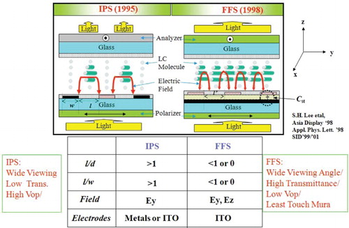
Although both the IPS and MVA modes were mainly used by several companies for both the monitor and TV applications at that time, these authors (engineers in the LCD division of Hyundai Electronics Co., now called “HYDIS Co.”) believed that both modes have intrinsic problems, such as low transmittance and high operating voltages, which are certainly not suitable for portable display application. Especially, when these authors fabricated a 12.1 IPS TFT-LCD, it was realized that the device showed an excellent viewing angle but its transmittance was very low with a relatively high operating voltage, such that the conclusion that both modes were not suitable for portable displays was arrived at. Therefore, all kinds of LC modes were tested, along with various electrode structures, to find an optimal solution to the problem of the IPS mode. The fringe-field switching (FFS) idea was then conceived, and its first patent was filed in 1996 [Citation9]. compares the electrode structures of the two modes. The key concept of the IPS mode is the in-plane field driving of homogenously aligned LC molecules. To reorient the LC director by in-plane field, the distance (l) between the electrodes should be larger than the electrode width (w) and cell gap (d). These approaches have two demerits. First, the LC director above the electrodes cannot rotate enough, and as such, transmittance loss above the electrodes cannot be avoided. Second, the operating voltage (Vop) of the IPS device is proportional to l/d; that is, it has a larger l, which will give rise to a higher transmittance, but its Vop will also be higher. Therefore, achieving IPS-LCDs with high transmittance and low Vop at the same time is not possible intrinsically. In the FFS mode, such an intrinsic problem is overcome. By positioning the pixel and common electrodes very close to each other under the electrode conditions (i.e., l/w and l/d<1) or by discarding the conventional l concept such that only the distance (l′) between the pixel (common) electrodes exists (l=0 μm), a strong in-plane field that can rotate the LC director will exist between the pixel and common electrodes, and thus, the LC director just above the electrode surface will rotate enough to be able to rotate the LC director above the center of the electrodes, where there is no in-plane field at all. In this way, the LC director above the whole electrode surfaces will rotate, giving rise to a high transmittance in all positions. Therefore, it can be concluded that the LC director in the FFS mode is switched by two mechanisms: first, by the dielectric torque between the LC director and the field, and then by the elastic torque between the LC director at the edge of the electrodes and the LC director at the center of the electrodes [Citation10]. In addition, the field intensity of the FFS mode just above the electrode surface is very strong compared to that of the IPS mode. For example, when Vop is 5 V, with l=5 μm, the maximum field intensity felt by the LC is 1 V/ μm in the IPS mode whereas it is 10 V/ μm (or 5 V/ μm when l exists) in the FFS mode because the passivation layer between the pixel and common electrodes is about 0.5 μm (or 1 μm when l exists). In other words, the Vop of the FFS mode is much lower than that of the IPS mode. Therefore, the FFS mode can realize a high transmittance and a low Vop simultaneously while still exhibiting a wide viewing angle owing to the in-plane rotation of the LC director, which opened a possibility for the FFS mode to be applicable to all kinds of high-performance displays, whether portable or non-portable. Another great advantage of the FFS mode is its self-forming storage capacitor (Cst), in which the Cst is formed in a light-transmitted area without sacrificing any aperture ratio while all the conventional LC modes need an area for Cst, which sacrifices an aperture ratio. This is another main reason that the FFS mode is a suitable one for high-resolution LCDs. Although it seems that the FFS mode very clearly reveals high electro-optic performances, it has one demerit: it requires two transparent electrodes, unlike the other LC modes TN, IPS, and MVA, which require only one transparent electrode in the TFT substrate.
Figure 1. Schematic comparison of the electrode structures of the IPS and FFS modes.
Hereafter, the main milestone of the FFS mode will be discussed.
1.1. First development stage of the FFS mode
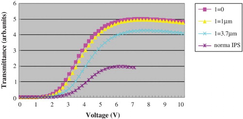
The first feasibility of the FFS mode was tested using the conventional 12.1 TN TFT-LCD by changing a few masks for the FFS TFT-LCD. One active area was divided into four parts: (1) the 1st ITO with a plane shape; and (2–4) the 1st ITOs with slit shapes. The first prototype was working fine while showing a much higher transmittance than the IPS-LCD, as presented in . The transmittance of the FFS mode with l=0 μm or 1 μm showed the highest transmittance when an LC with negative dielectric anisotropy (−LC) was used. When the feasibility of the FFS LCD was confirmed in 1998, a 15.0
XGA TFT-LCD using an LC with negative dielectric anisotropy was developed for monitor displays. Interestingly, the device showed the best transmittance among the wide-viewing-angle LCDs at that time, and as such, it was said to be the device that shows a wide viewing angle and a high transmittance at the same time in the authors’ talk upon the invitation of Asia Display [Citation11–13].
Figure 2. Measured voltage-dependent transmittance curves of the FFS mode with four different electrode structures and of the IPS mode using a 12.1′′ TFT-LCD. Here, the IPS and FFS modes use a LC with positive and negative dielectric anisotropies, respectively.
Another unique and interesting performance aspect of the LCD was found. That is, the display almost did not show ripples and pooling mura or pushed marks at all when an external pressure was applied to the panel device with the fingers or a pen [Citation14,Citation15]. In the case of the TN mode, strong ripples can be easily observed when pressure is applied to the panel, and in the case of most VA modes, relatively strong pooling mura can be observed. At that time, Wacom Co., which makes pen-based 3D input displays for animation drawing works in Hollywood movies noticed the strong merit of the FFS displays and commercialized them for display application for the first time. When the company used the FFS mode, the demerits of the conventional display, which requires a thick cover glass with an air gap between the panel and the cover glass, causing image parallax to occur with weight and system cost increases while decreasing the transmittance, were overcome. They thus received major compliments from their customers, as follows: “Tablets with conventional LCDs have a parallax issue and feel like drawings on a glass, but with the FFS Tablet PC, there is no parallax issue, and we feel like we are drawing on a piece of paper.” In fact, this pen-based display indicates that the FFS-LCD is suitable for the touch screen display, which is a required function in all portable displays. This fact was already recognized in 1998.
1.2. Second development stage of the FFS mode
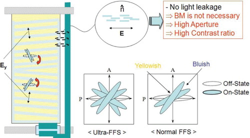
Since the mid-1990s, the size of the TFT-LCDs for monitor use has become increasingly bigger than 17, and the monitor has also come to play the role of a TV at the same time. The first FFS-LCD used a −LC with a rather high cost and a much larger rotational viscosity than that of the LC with positive dielectric anisotropy (+LC). Moreover, the magnitude of its dielectric anisotropy for a commercialized −LC mixture is much lower than that of +LC. Therefore, the FFS-LCD with −LC would show a slower response time and a higher operating voltage than that with +LC. If a +LC with IPS mode concepts will be used, however, the transmittance of the FFS-LCD will no longer be excellent, and a certain level of pooling mura will appear. At that time, there were extensive studies regarding what determines the transmittance of the FFS-LCD with +LC, and it was found that the light efficiency of the LC mode was dependent on many cell parameters, such as the LC's retardation [Citation16], the cell gap [Citation17], the electrode structure [Citation18], and the magnitude of dielectric anisotropy [Citation19]. In addition, it is widely known that the transmittance of the LCD is dependent not only on the LC's light efficiency but also on the pixel aperture ratio. As such, all the panel and cell parameters were optimized to maximize the performance of the FFS-LCD with +LC, and “U-FFS” [Citation20], which exhibits the following properties, was proposed:
high transmittance;
high contrast in a wide range;
minimized color shift;
fast response; and
low power consumption.
As presented in for the pixel structure, the pixel electrode has a wedge shape with a symmetry line in the horizontal direction, so that the initial LC orientation is in a horizontal direction, consistent with the field direction between the data line and the pixel electrodes, which can keep an original dark state. Owing to such characteristic, the width of the black matrix on the top substrate can be minimized, resulting in a maximized aperture ratio. The proposed concept becomes the basis of all FFS-LCDs, including the tablet PCs in early 2000, the black-and-white displays for medical uses, and the monitors and LCD-TVs in the mid-2000s.
Figure 3. Schematic pixel structure of the U-FFS LCD.
1.3. Third development stage of the FFS mode
In the early 2000s, tablet LCDs with a pen-based system with the TN mode already existed, but the TN mode had a very narrow viewing angle, which was not suitable for the tablet PC because it could be displayed in either the landscape or portrait type depending on the user's preference. In addition, the device must be high-resolution, like XGA in the 12.1 display, so that maximizing the transmittance while keeping a wide-viewing angle and a low operating voltage was very important for high-performance LCDs with a high image quality and low power consumption. As the pixel size became smaller, the unwanted field direction around the corners of the pixel electrode no longer became negligible, and the stability of the LC's reorientation with +LC when an external pressure was applied was not satisfactory enough. A better pixel structure, which solved this problem, and maximized transmittance in relatively high-resolution FFS-LCDs were proposed as A-FFS [Citation21]. In the mid-2000s, Hydis Co. and Seiko Epson tried to apply the FFS mode to super-high-resolution mobile LCDs. Then they proposed a revolutionary pixel structure that maximizes the transmittance in the FFS mode, the so-called “H-FFS” [Citation22]. As clearly shown in , the transmittance of the 2.0
QVGA HFFS-LCD was improved by more than 50% compared to that of the AFFS-LCD, and was even higher than that of the TN-LCD.
Figure 4. Comparison of the voltage-dependent transmittance curves in high-resolution mobile TFT-LCDs. The HFFS mode shows a much improved transmittance, as also shown in the microscopic image of a pixel [Citation21] and see also the website of HYDIS Co.
![Figure 4. Comparison of the voltage-dependent transmittance curves in high-resolution mobile TFT-LCDs. The HFFS mode shows a much improved transmittance, as also shown in the microscopic image of a pixel [Citation21] and see also the website of HYDIS Co.](/cms/asset/fa7a122f-f070-42d0-8b90-2134c3452f2a/tjid_a_914982_f0004_c.jpg)
The key feature of the structure is that the common electrode exists above the pixel electrode, unlike that in the conventional AFFS mode, and covers the data line to shield off any noise field coming from the data line, so that the transmittance near the data line is maximized by removing the LC's disclination lines and minimizing the width of the black matrix on the top substrates, as indicated in . The HFFS structure has become the foundation of all the present high-resolution FFS (IPS) LCDs, from small-to-medium-sized displays.
Figure 5. Schematic comparison of the pixel structures and simulated transmittances of the AFFS and HFFS modes [Citation21].
![Figure 5. Schematic comparison of the pixel structures and simulated transmittances of the AFFS and HFFS modes [Citation21].](/cms/asset/7b4f78af-de61-4927-a048-64c3e99a5a2f/tjid_a_914982_f0005_c.jpg)
2. Historical movement of the FFS mode
2.1. First movement
The FFS mode overcomes the long-standing problems of the IPS mode. Nevertheless, the FFS mode was not adopted by other major companies until 2004. Instead, Hitachi Co. continuously reported the improved performance of the IPS TFT-LCD and S-IPS in 1998 and of the AS-IPS in 2002. The AS-IPS used an organic resin to improve the transmittance, which was not an easy process at that time. In addition, the resin was opened between the electrodes and can become a source of ions, causing image sticking. If the FFS mode is adopted without using resin, however, its transmittance will be higher than that of the AS-IPS, with a lower operating voltage. Consequently, Hitachi Co. adopted a new IPS, with the same concept as that of the FFS mode (they named it “IPS-Pro”), in 2004 [Citation23], which surprised the world's display industries. The FFS mode was then noticed more by other companies.
2.2. Second movement
The major expert company for small LCDs in the early 2000s was Seiko-Epson Co. The company also adopted the HFFS mode for their super-high-resolution mobile LCDs in 2006, which marked FFS's first application to mobile LCDs with high-resolution LCDs.
2.3. Third movement
Until the first and second historical movements, the FFS mode was still not in the main LC mode because the biggest LCD companies, such as LGD, Samsung, Sharp, and AUO, did not use the FFS mode, although LGD used the FFS mode for its mobile LCDs. In 2010, revolutionary products called “iPhone4 Retina Display” and “iPad” were released by Apple Co. At that time, the required resolution of the retina display was the highest, 326 ppi, while keeping low power consumption and high image quality. On the other hand, the required electro-optic performances of the iPad product were as follows: 10-h use without recharging the battery, wide-viewing angle, and touch screen display. According to the analyses conducted by Apple Co., the FFS-LCD best met their requirements, and as such, the LCD panel maker LGD started its mass production with the FFS mode for the iPhone and iPad. Since then, the FFS-LCD has become the symbol of the high-resolution and high-performance TFT-LCDs.
3. Popularity of the FFS LC mode: the present
When Apple Co. used the FFS mode for its products with a high resolution, high image quality, low power consumption, and touch screen displays, the merits of the FFS mode were recognized by many other companies. Trials were conducted to meet such requirements using the conventional IPS and MVA modes, but the performances of such modes could not meet the level of the FFS mode.
Since 2010, most of the high-resolution and high-image-quality LCDs for mobile phones and tablet PCs have adopted the FFS mode. On the other hand, TN and WV-TN were the main LC modes for the notebook and monitor displays. As the display resolution became increasingly higher for high image quality, however, the transmittance of the TN mode was not better than that of the FFS mode, and the viewing angle characteristics and touch screen suitability of the TN mode were inferior to those of the FFS mode. Since recently, the most important keyword in displays has become “high resolution” because the display image quality in the normal direction purely depends on the resolution, irrespective of the display mode or type. From this viewpoint, the FFS mode is the most suitable mode because it exhibits the highest transmittance among all the LC modes, especially in LCDs with a high resolution. On the other hand, the LCDs are competing with the emissive OLEDs, whose image quality does not have many viewing angle issues. Consequently, using only the TN mode cannot realize high-performance LCDs, as above-mentioned, and as such, the TN mode is currently being replaced by the FFS mode even in notebooks and monitors. When the HFFS mode is used for large super-high-resolution FFS-LCDs, however, the electrical load becomes too high, which makes driving very difficult. As a result, several companies, including Panasonic LCD Co., proposed a new electrode structure employing an organic resin above the data line, and the plane shapes of the common electrodes covered all the signal lines to shield any noise electric field coming from the TFT, as shown in [Citation24,Citation25]. In , the insulator between the data line and the common electrode is not indicated as an organic resin, but for large (over 10) and super-high-resolution TFT-LCDs, organic resin is suitable for the over-1-μ m layer. Panasonic LCD Co. claimed that the high-transmittance FFS-LCD can be realized even if the display resolution increases from the full-HD to the 4K2K proposed structure, as shown in . Even if the resolution is increased fourfold, the width of the black matrix on the top substrate can be reduced with the proposed structure, so that the aperture ratio is maintained at 70%, which is about the same value of the full-HD structure. In the conventional LCD concepts and approaches, this is not imaginable; that is, only the FFS mode, which has an optimized pixel structure, can open a new paradigm: that increasing the resolution of LCDs fourfold will not decrease the aperture ratio. For LCD-TVs, Japan/Panasonic LCD Co. and BOE Co. have adopted the FFS mode for their LCD-TVs. In addition, BOE Co. recently reported the largest 110
UD TFT-LCD with the FFS mode, with the following panel specifications:
nits; contrast
; response time=6 ms (G to G); and frame
Hz [Citation26]. Surprisingly, a-Si for TFT and aluminum (Al) metal for signal lines are used even with the 110
LCD display.
Figure 6. Comparison of the pixel structures of the IPS-Pro and IPS-Pro Next pixels [Citation23,Citation24].
![Figure 6. Comparison of the pixel structures of the IPS-Pro and IPS-Pro Next pixels [Citation23,Citation24].](/cms/asset/049b2113-bacb-4eeb-9b60-f9249bb1ff4c/tjid_a_914982_f0006_c.jpg)
Figure 7. Comparison of the pixels of the 47′′ IPS-LCDs [Citation24].
![Figure 7. Comparison of the pixels of the 47′′ IPS-LCDs [Citation24].](/cms/asset/bbfaa17d-d8e9-4243-b54f-03a365987261/tjid_a_914982_f0007_c.jpg)
To conclude, all the current high-resolution and high-performance LCDs, from the small to the medium-sized ones (less than 30), are mainly using the FFS mode, and surprisingly, most of the major LCD companies at present are using the FFS mode for such applications, although they use different names for it, such as IPS-Pro, Photo Fine Vistarich, AH-IPS, PLS, and ADS.
4. Technical issue of the present FFS-LCD
4.1. LC
At present, most of the FFS LCDs use a +LC because it offers a lower operating voltage, a faster response time, and a lower cost than a −LC. The transmittance, however, becomes more critical as the resolution of LCDs becomes higher — i.e., over 500 ppi for the mobile and retina displays of medium-sized displays. To maintain the high transmittance of the FFS-LCD even in super-high-resolution LCDs, a −LC is favored, even though its response time will be slower and its operating voltage will slightly increase. Therefore, further optimization of the cell parameters and LC materials is absolutely required for the high-transmittance and fast-response-time FFS-LCD with −LC [Citation27].
4.2. Non-contact LC alignment
The FFS-LCD requires a homogenous LC alignment with a zero pretilt angle. Most of the FFS-LCDs are made with a rubbing process so that rubbing-related defects always exist, resulting in a decrease in the contrast ratio of the LCD. Moreover, the rubbing generates a 1–2 ° surface pretilt angle. Therefore, this rubbing process should be replaced by a non-contact LC alignment process. Several types of photoalignment layers are currently being tested, and Panasonic LCD Co. reported photoaligned IPS-LCDs for TV use, which showed a 1700:1 contrast ratio [Citation28,Citation29].
4.3. Further optimization of electro-optic performances
The FFS mode shows some unusual electro-optic behavior so that the DC-driven voltage-dependent transmittance curve between the positive and negative frames does not perfectly match, unlike in the other conventional LC modes. In addition, low-frequency driving, such as at 5 Hz, generates flickering. Further extensive studies are thus required to fully understand this behavior. In addition, especially when a −LC is used, a thin cell gap (less than 3 μm) and fine electrode patterning (close to 2 μm) are strongly favored to achieve fast-response-time and high-transmittance FFS-LCDs [Citation27,Citation30].
4.4. Charging issue in large LCD-TVs
The FFS mode has a great advantage in the pixel aperture ratio because of its self-formed storage capacitor, as mentioned earlier. The Cst might become too big, however, when the pixel size is quite large, as in the LCD-TV, and thus, a charging issue appears. Although this kind of intrinsic difficulty exists, BOE Co. already proved the perfect driving of 110 UD FFS-LCD using an a-Si TFT, which implies that the intrinsic problem can be overcome with the optimization of the panel and driving. To solve the charging issue, an oxide TFT with high mobility needs to be adopted, and the pixel structure needs to be optimized, especially in large FFS-LCDs.
5. Vision of the FFS LC mode: the future
The FFS-LCD is continuously evolving to exhibit better performance as well as low cost, targeting better performance in electro-optics and lower cost over the emissive OLEDs. Looking back on the major historical movement of the FFS-LCD since it was first reported to the public in 1998, every six years, a great event occurred, such as that the Hitachi LCD-TVs adopted the FFS in 2004 and Apple iPad adopted the FFS mode in 2010. It is hoped that eco-friendly green FFS LCD-TVs with photoalignment, oxide TFTs, and a revolutionary LC mixture will become the main trend even in the LCD-TVs that will be produced by many companies in 2016.
Acknowledgement
This work was supported by the National Research Foundation (NRF) of Korea and the Korea-China Joint Research Program under grant no. 2012-0004814.
References
- M. Schadt and W. Helfrich, Appl. Phys. Lett. 18, 127 (1971). doi: 10.1063/1.1653593
- S.H. Lee, S.S. Bhattacharyya, H.S. Jin and K.U. Jeong, J. Mater. Chem. 22, 11893 (2012). doi: 10.1039/c2jm30635b
- H.S. Kwok, S. Naemura and H.L. Ong, Progress in Liquid Crystal Science and Technology: in Honor of Shunsuke Kobayashi's 80th Birthday (World Scientific’13, Singapore) Series on Liquid Crystal 4 (2013).
- M. Oh-e, M. Ohta, S. Aratani and K. Kondo, in Proceedings of the 15th International Display Research Conference (Asia Display) (1995), p. 577.
- M. Ohta, M. Oh-e and K. Kondo, in Proceedings of the 15th International Display Research Conference (Asia Display) (1995), p. 707.
- M. Oh-e and K. Kondo, Appl. Phys. Lett. 67, 3895 (1995). doi: 10.1063/1.115309
- Y. Koike, S. Kataoka, T. Sasaki, H. Tsuda, A. Takeda and K. Ohmuro, in Proceedings of the 4th International Display Workshops (1997), p. 159.
- A. Takeda, S. Kataoka, T. Sasaki, H. Chida, H. Tsuda, K. Ohmuro, T. Sasabayashi, Y. Koike and K. Okamoto, SID Symp. Digest Tech. Pap. 29, 1077 (1998). doi: 10.1889/1.1833672
- S.L. Lee and S.H. Lee, KR Patent No. 19,960,059,509 (2000).
- S.H. Jung, H.Y. Kim, M.-H. Lee, J.M. Rhee and S.H. Lee, Liq. Cryst. 32, 267 (2005). doi: 10.1080/02678290412331329233
- S.H. Lee, S.L. Lee and H.Y. Kim, in Proceedings of the 18th International Display Research Conference (Asia Display) (1998), p. 371.
- S.H. Lee, S.L. Lee and H.Y. Kim, Appl. Phys. Lett. 73, 2881 (1998). doi: 10.1063/1.122617
- S.H. Lee, S.L. Lee, H.Y. Kim and T.Y. Eom, SID Symp. Digest Tech. Pap. 30, 202 (1999). doi: 10.1889/1.1833995
- S.H. Lee, H.Y. Kim, S.M. Lee, S.H. Hong, J.M. Kim, J.W. Koh, J.Y. Lee and H.S. Park, J. Soc. Inf. Display 10 (2), 117 (2002). doi: 10.1889/1.1827852
- J.D. Noh, H.Y. Kim, J.M. Kim, J.W. Koh, H.S. Park and S.H. Lee, in Proceedings of the 2nd International Display Manufacturing Conference (2002), p. 447.
- I.H. Yu, I.S. Song, J.Y. Lee and S.H. Lee, J. Phys. D: Appl. Phys. 39, 2367 (2006). doi: 10.1088/0022-3727/39/11/009
- H.Y. Kim, S.H. Hong, J.M. Rhee and S.H. Lee, Liq. Cryst. 30, 1285 (2003). doi: 10.1080/02678290310001605893
- I.H. Yu, I.S. Song, J.Y. Lee and S.H. Lee, J. Phys. D: Appl. Phys. 39, 2367 (2006). doi: 10.1088/0022-3727/39/11/009
- J.W. Ryu, J.Y. Lee, H.Y. Kim, J.W. Park, G.D. Lee and S.H. Lee, Liq. Cryst. 35, 407 (2008). doi: 10.1080/02678290801919659
- S.H. Lee, S.M. Lee, H.Y. Kim, J.M. Kim, S.H. Hong, Y.H. Jeong, C.H. Park, Y.J. Choi, J.Y. Lee, J.W. Koh and H.S. Park, SID Symp. Digest Tech. Pap. 32, 484 (2001). doi: 10.1889/1.1831901
- Y. Nakayoshi, N. Kurahashi, J. Tanno, E. Nishimura, K. Ogawa and M. Suzuki, SID Symp. Digest Tech. Pap. 34, 1100 (2003). doi: 10.1889/1.1832480
- D.H. Lim, H.Y. Lee, J.P. Kim, K.J. Lee, H.J. Yun, K.Y. Han, Y.H. Jeong, in Proceedings of the 13th International Display Workshops (2006), p. 807.
- K. Ono, I. Mori, Y. Tomioka and Y. Satou, in Proceedings of the 15th International Display Workshops (2004), p. 295.
- K. Ono and I. Hiyama, in Proceedings of the 19th International Display Workshops in Conjunction with Asia Display (2012), p. 933.
- K. Ono and H. Matsukawa, in Proceedings of the 20th International Display Workshops (2013), p. 24.
- Y.P. Liao et al., in Proceedings of the 13th International Meeting on Information Display (2013), p. 11.
- H.J. Yun, M.H. Jo, I.W. Jang, S.H. Lee, S.H. Ahn and H.J. Hur, Liq. Cryst. 39, 1141 (2012). doi: 10.1080/02678292.2012.700078
- H.J. Ahn, C. Lim, D. Kim, J. Lee, H. Park, S. Lee, J. Woo, W. Shin and M. Jun, SID Symp. Digest Tech. Pap. 44, 1432 (2012). doi: 10.1002/j.2168-0159.2012.tb06077.x
- H. Matsukawa, Y. Shimano, M. Suefuji, Y. Umeda and K. Mimura, in Proceedings of the 19th International Display Workshops in conjunction with Asia Display (2012), p. 1581.
- S.H. Lee, SID Seminar note, M4 (2013).