
Abstract
We demonstrated self-aligned amorphous-Indium-Gallium-Zinc-Oxide (a-IGZO) thin-film transistors (TFTs) where the source–drain (S/D) regions were made conductive via chemical reduction of the a-IGZO via metallic calcium (Ca). Due to the higher chemical reactivity of Ca, the process can be operated at lower temperatures. The Ca process has the additional benefit of the reaction byproduct calcium oxide being removable through a water rinse step, thus simplifying the device integration. The Ca-reduced a-IGZO showed a sheet resistance (RSHEET) value of 0.7 kΩ/sq., with molybdenum as the S/D metal. The corresponding a-IGZO TFTs exhibited good electrical properties, such as a field-effect mobility (μFE) of 12.0 cm2/(V s), a subthreshold slope (SS−1) of 0.4 V/decade, and an on/off current ratio (ION/OFF) above 108.
1. Introduction
In recent years, amorphous oxide semiconductors (AOSs) have emerged as alternative materials for amorphous silicon thin-film transistor (TFT) in display backplane manufacturing. These materials demonstrate significant advantages, including high uniformity, high electron mobility, and the ability to be fabricated at temperatures compatible with plastic substrates. Among these AOSs, amorphous-Indium-Gallium-Zinc-Oxide (a-IGZO) is very promising for the fabrication of a new generation of active TFTs for use in transparent displays, touch screens, smart windows, and other devices on flexible and rigid substrates [Citation1–4]. Future display backplane generations with increasing resolutions (e.g. 3640 × 2160 pixels) and frame rates (120 or 240 Hz) require high speed TFTs. The established back-channel-etch and etch-stop-layer configuration-based TFTs are less suitable for such applications due to their high parasitic capacitance caused by the overlap between the source and drain electrodes (S/Ds) and the gate electrode [Citation5, Citation6]. The self-aligned (SA) TFT configuration presents benefits such as reduced overlap capacitance and a smaller footprint, and is therefore preferred. The S/D region conductivity enhancement is one of the major integration challenges in this configuration. Various research groups have reported integration techniques for enhancing the conductivity of these S/D regions. For example, Ye et al. and Chen et al. reported high-performance SA TFTs with S/D regions implanted with boron, phosphorus, and arsenic [Citation7–9]. In this approach, the high temperature anneal (>400°C) for dopant activation could be an integration challenge for the temperature-sensitive AOS materials. The integration of such TFT process flow in plastic substrates constitutes another challenge. Mourey et al. reported SA TFTs that use backside exposure for conductivity enhancement of S/D regions [Citation10]. In this approach, the optical absorption of the substrate and the material stack might be disadvantageous for the process. Furthermore, thermal and bias stress stabilities could be other issues caused by this process. In another approach, Kim et al. and Ahn et al. reported argon (Ar) and hydrogen (SiH4 and NH3) plasma treatments for the conductivity enhancement of the S/D regions [Citation11–14]. Although the integration of this approach in the process flow is straightforward, the corresponding transistors might suffer from degradation when submitted to thermal treatments at 250°C or higher temperatures. This can be attributed to the unstable diffusion profiles of hydrogen in the case of the hydrogen plasma and the recovery of the generated defects (an In-rich surface) in the case of the Ar plasma. Furthermore, Morosawa et al. reported SA TFTs with a-IGZO where the S/D regions were reduced by metallic Ti and Al [Citation15]. The process involves deposition of a very thin layer (5–10 nm) of the metal, followed by a high stemperature anneal (>300°C) to form their oxides. During this process, the a-IGZO of the S/D regions is partly chemically reduced, leading to a local increase in conductivity. The uniformity of the thin metal layer over the large substrate size, the high temperature (≥250°C) requirement for the chemical reaction between a-IGZO and the metal, and the removal of the formed metal oxide might complicate the integration into the process flow. All these complications can be avoided using the alkaline earth metal calcium (Ca) as a reducing agent [Citation16]. The reduction of a-IGZO occurs during Ca deposition and the following thermal treatment at 240°C in a N2 ambient oven, which yields S/D regions that consist of highly conductive a-IGZO.
Figure 1. (a) Cross-sectional scheme and (b) optical micrograph of SA a-IGZO TFTs.
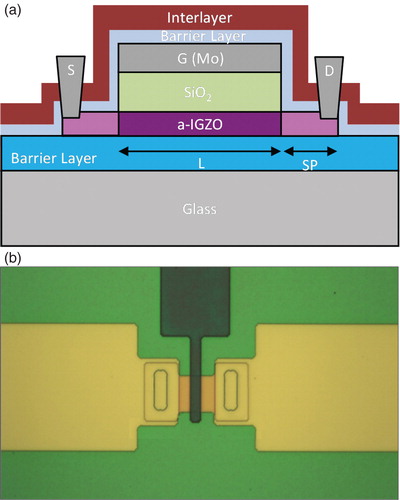
Figure 2. (a) Transfer (VGS−IDS) and (b) output (VDS−IDS) characteristics of SA TFTs with W = 15 µm, L = 5 µm, and SP = 10 µm.
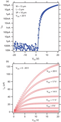
Figure 3. Dependence of the RSHEET of hydrogen plasma, Ar plasma, and Ca-treated a-IGZO on the channel length at V = 2.0 V. The layout of the resistor structure is shown in the inset.
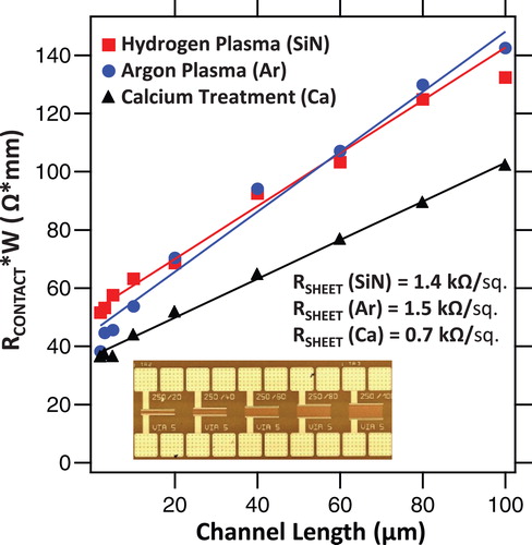
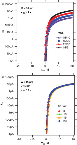
Figure 4. Transfer (VGS−IDS) characteristics dependence on (a) ‘L’ scaling and (b) ‘SP’ scaling of SA TFTs.
2. Experiment details
In the first step, a barrier film was deposited on a glass substrate [Citation17]. On top of this barrier film, an IGZO layer was deposited via DC sputtering. The a-IGZO layer was patterned via wet chemical etching, followed by deposition of the gate dielectric (200 nm SiO2 via plasma enhanced chemical vapor deposition (PECVD) at 250°C) and the gate metal layer [100 nm of molybdenum (Mo) via DC sputtering]. The gate stack (metal and dielectric) was patterned using the dry etching process. In the next step, the Ca metal layer was deposited on the now exposed S/D regions that abutted from the patterned gate stack through evaporation, and the treated substrate was annealed on a hot plate at 250°C in a N2 atmosphere. This was followed by a water rinse that removed the unreacted Ca and the other byproducts. The entire device was capped with a stack of barriers and an inter-metal layer (200 nm PECVD SiO2), followed by contact opening with a dry etching step. Mo (100 nm) was deposited via sputtering to form interconnects, and patterned by dry etching. Finally, the TFTs were annealed at 240°C in an N2 ambient oven for one hour. All the processes were performed at a temperature below 250°C to enable integration on the polyimide foil and a range of potential moisture barriers [Citation17]. The current–voltage (I–V) characteristics of the individual TFTs were measured using an Agilent 4156 parameter analyzer.
3. Results and discussion
A schematic cross-section and optical micrograph of an integrated SA a-IGZO TFT is shown in . The typical transfer and output characteristics of the fabricated SA a-IGZO TFTs with W = 15 µm, L = 5 µm, and SP = 10 µm are shown in (a) and (b), respectively. The figures of merit of such TFTs at a drain-to-source voltage (VDS) of 20 V are a μFE of 12.0 cm2/V s, an SS−1 of 0.4 V/dec, and an ION/OFF ratio of ∼4.9 × 10⁸. The sheet resistivity of <1.0 kΩ/sq. was required for the a-IGZO spacing (SP) between the gate and the metal interconnects, to prevent degradation of the aforementioned values (to maintain Rchannel > Rcontact). The aforementioned Ca treatment resulted in a sheet resistivity (RSHEET) value of 0.7 kΩ/sq. The treatment is a chemical oxide-reduction reaction of the alkaline earth metal with the metal oxide semiconductor layer, additional details of which have been published [Citation16]. In this method, when a reducing layer of an alkaline metal (e.g. any one of, or any combination of, Li, Na, K, Rb, Cs, or Fr) or an alkaline earth metal (e.g. any one of, or any combination of, Be, Mg, Ca, Sr, Ba, or Ra) come in physical contact with the metal oxide semiconductor layer, a chemical reduction reaction is initiated between the reducing layer and the metal oxide semiconductor layer. The reduction reaction affects the chemical composition of the metal oxide semiconductor layer, for instance, by decreasing the oxygen content. The treatment is completed by a rinsing step with water, in which the excess of the reducing layer and the reaction byproducts are washed away. Through this treatment, the sheet resistivity decreased from above 100 kΩ/sq. for the as-deposited a-IGZO film to 0.7 kΩ/sq. for the Ca-treated film. This low sheet resistivity even remained unaffected by an additional post anneal at 240°C in an N2 ambient oven. In ,
Figure 5. (a and c) Evolution of the transfer characteristics (VGS−IDS) of SA TFTs (W = 15 µm and L = 5 µm) as a function of the duration time at +1.0 MV/cm (VGS = +20 V and VDS = 0 V) and at −1.0 MV/cm (VGS = −20 V and VDS = 0 V). (b and d) VTH shift as a function of the stress time in the positive and negative directions.
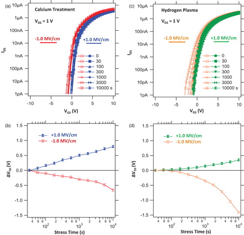
show the resistivity of the treated a-IGZO using separate resistor structures (figure inset) with different channel lengths (L) and a constant width (W). This method leads to the extracted RSHEET value of 0.7 kΩ/sq. We also compared it with the standard hydrogen plasma (SiNx interlayer) and the Ar plasma-treated a-IGZO, and measured the values of 1.4 and 1.5 kΩ/sq., respectively. The contact resistance between the interconnect metal and the treated a-IGZO was extracted by extrapolating the lines to the zero channel length, and was equal to the RCONTACT W = 3.8 Ω cm. The output characteristic [(b)] depicted clear linear regions and did not show s-shaped behavior at a low VDS, which indicates that no Schottky barrier at the S/D contacts was obtained. Furthermore, to verify that the RSHEET of the gate-source contact is well distributed across the channel SP and the channel length and does not limit the TFT performance, the transfer characteristics (at VDS = 1 V) of the TFTs with different spacings between their channel and interconnects (SP = 8, 10, 15, and 20 µm) and with different channel lengths (L = 40, 20, 10, and 5 µm) are compared in (a) and (b), respectively. From (a), it is clear that the SP length of 8–20 µm did not result in a change in the TFT characteristics, meaning that the resistivity of the S/D regions is well distributed over a wide SP range and low enough for the total device resistance to be dominated by the resistivity of the channel. For the TFTs with the shortest channels, that is, 5 µm, no degradation of the mobility and subthreshold slope (SS−1) was observed, as shown in (b). This indicates that no lateral diffusion of the Ca treatment into the channel region occurred, which can cause channel shortening effects. In reference [Citation16], the effect of the a-IGZO thickness on the Ca treatment is described. It shows that the effect of the Ca treatment is very strong for thin a-IGZO layers (13 nm) and stabilizes for thicker a-IGZO layers (26, 40, and 60 nm). This is a clear indication that the effect of the Ca treatment affects up to a maximum 20–30 nm of a-IGZO. This is also in line with the time-of-flight secondary ion mass spectrometry analysis, demonstrating that traces of Ca within the a-IGZO decrease very strongly within the first 20–30 nm of a-IGZO [Citation16]. Since a-IGZO is amorphous, the channel region must be affected in a similar way in all directions. Assuming that a-IGZO would be affected to 50 nm (instead of the aforementioned 20–30 nm), the channel should shorten by a maximum of 100 nm (2 × 50 nm), which is negligible for a 5 µm channel length (and likely also below the reproducibility range of the lithographic process). Furthermore, in , we report the bias stress behavior of the TFTs as a function of the stress time. The TFTs were stressed at a field strength of +1 MV/cm (VGS = +20 V and VDS = 0 V) in the positive direction, and at a field strength of −1 MV/cm (VGS = −20 V and VDS = 0 V) in the negative direction at room temperature for a period of 104 seconds. The evolution of the transfer characteristics (VGS−IDS) of the TFT (W = 15 µm, L = 5 µm, and SP = 10 µm) as a function of the duration time is shown in (a). The linear mobility of 12 cm2/(V s), the SS–1 of 0.4 V/decade, and the ION/OFF ratio of above 108 were very similar before and after the stressing, but a constant VTH change of less than 1.2 V was observed in both the positive and negative directions, as shown in (b). This shift should not be related to the Ca treatment because similar results have been observed when hydrogen plasma (SiNx Interlayer) was used to enhance the conductivity of S/D regions [(c) and (d)] using an identical gate stack formation process. The small differences in the shifts could have been due to the different integration steps used in the stacks, but the overall VTH shifts in both cases was most probably related to the interface change between a-IGZO and the gate dielectric layer (SiO2). As mentioned, a low-temperature (250°C) SiO2 was used as the gate dielectric layer. Normally, at this temperature, PECVD SiO2 films suffer a high hydrogen content and poor passivating properties, which contribute to bias stress shift issues [Citation6]. Longer anneal times and high temperature gate dielectrics might result in better bias stabilities.
4. Conclusion
In summary, we successfully fabricated SA a-IGZO TFTs with S/D regions treated with Ca. The TFTs showed a field-effect mobility of 12.0 cm2/(V s), a SS−1 of 0.4 V/decade, and an ION/OFF ratio above 108. Thus, the low-temperature formation of S/D contacts in the SA a-IGZO TFT technology was demonstrated.
Acknowledgements
This work was performed in a collaboration between IMEC and TNO in the frame of the HOLST Centre.
Additional information
Manoj Nag is a Senior Scientist at IMEC, Belgium, involved in the development of metal-oxide-based TFTs for thin-film circuits and AMOLED backplanes on rigid and flexible substrates. He received his Master of Technology (Solid-state Materials) degree at the Indian Institute of Technology in Delhi, India, in 1998. From 1999 to 2005, he worked as a Senior Process Engineer in ST Microelectronics (Singapore); from 2005 to 2007, as a Senior Process Engineer at International Rectifier Newport (UK); and from 2007 to 2009, as a Technology Transfer Module Leader for Integration at Qimonda AG in Germany. He is currently working on his Ph.D. thesis on the ‘Bias Stress Stability of Oxide Semiconductor-based TFTs’ at IMEC in Belgium and at the Electrical Engineering Department of K.U. Leuven, also in Belgium.
Robert Muller received his Ph.D. degree in Sciences (Chemistry) from the Facultés Universitaires N.D. de la Paix in Namur, Belgium, in 1995, for his ultramicroelectrode study of electrochemically active organic molecules. Afterwards, he taught chemistry-related courses at the Chemistry Department of the Facultés Universitaires N.D. de la Paix (Namur, Belgium, 1995–1996) before joining the Albert-Ludwigs Universität (Freiburg, Germany, 1996–1997) for a post-doc on fullerene electrochemistry. Between 1997 and 2003, he was an assistant at the Chemistry Department of the University of Liège in Belgium who taught organic, analytical, and general chemistry. In 2004, he joined IMEC and specialized in resistive switching organic memories (EC projects: NosceMemorias and EMMA), organic transistors (EC project: Polaric), and inorganic transistors (IGZO).
Soeren Steudel received his M.Sc. degree in Electrical Engineering from the Dresden University of Technology in Germany and his Ph.D. degree from the Katholieke Universite in Leuven, Belgium, in 2002 and 2007, respectively. He has been working at IMEC since 2002 on TFTs and rectifying diodes. This work resulted in more than 20 journal publications, several patents, and numerous conference contributions. His research interests include flexible backplanes for display application, and process integration of organic and metal oxide semiconductor and thin-film circuits on foil. He is currently the team leader for organic and oxide electronic devices at IMEC.
Steve Smout was born in Leuven, Belgium, on 17 March 1984. He received his B.Sc. degree in Chemistry in 2007 at the Katholieke Hoge School of Leuven (KH Leuven) in Belgium. He has since been working in the Large-area Electronics Department of IMEC in Belgium. His main expertize lies in the research, development, and integration of organic and inorganic semiconductors for display applications and photolithography.
Ajay Bhoolokam was born in Mysore, India. He earned his Bachelor's degree in Electronics and Communication at the Sri Jayachamarajendra College of Engineering (SJCE) in Mysore in 2006. He obtained his Master's degree in Nanoscience and Nanotechnology at KU Leuven in Belgium in 2011. He is currently working on his Ph.D. thesis on Oxide Semiconductors in the Large-area Thin-film Electronics group at IMEC.
Kris Myny was born in Hasselt, Belgium, on 26 July 1980. He received his Master's degree at the Katholieke Hoge School Limburg in Diepenbeek, Belgium, in 2002. He joined IMEC in Leuven in 2004 as a member of the Polymer and Molecular Electronics group. In 2008, he started working on his Ph.D. thesis on the design of organic circuits. His main research interests are the design, fabrication, and optimization of digital organic circuits, among other organic RFID tags and AMOLED backplanes. He was the recipient of the IMEC2010 Scientific Excellence Award.
Sarah Schols received the Master of Applied Science degree in Electrical Engineering (Option Nanotechnology) and a Ph.D. degree from the Katholieke Universite in Leuven, Belgium, in 2004 and 2009, respectively. Her doctoral research was funded by the Belgian Fund for Scientific Research (FWO) and focused on the design of new device architectures and material concepts for organic light-emitting devices. She is currently the Team Leader for Organic and Oxide Integration at IMEC in Leuven.
Jan Genoe was born in Leuven, Belgium, on 19 May 1965. He received his M.S. degree in Electrical Engineering and his Ph.D. degree from the Katholieke Universite in Leuven in 1988 and 1994, respectively. Afterwards, he joined the Grenoble High Magnetic Field Laboratory as a Human Capital and Mobility Fellow of the European Community. In 1997, he became a Lecturer at the Katholieke Hoge School Limburg (KHLim) in Diepenbeek, Belgium. Since 2003, he has been both a professor at KHLim and head of the Polymer and Molecular Electronics (PME) group of IMEC. His current research interests are organic and oxide transistors and circuits, as well as organic photovoltaics. He is the author and co-author of about 90 papers in refereed journals. Jan Genoe is a member of the IEEE.
Brian Cobb received his BS degree in Electrical Engineering in 2004 from the University of Virginia, and his M.S. and Ph.D. degrees in Solid-state Engineering from the University of Texas in Austin in 2006 and 2010, respectively. He currently works as a Research Scientist at the Holst Centre (an open collaboration between TNO and IMEC) in Eindhoven, the Netherlands.
Abhishek Kumar received his Bachelor's degree in Polymer Science and Chemical Technology from the Delhi College of Engineering in India in 2004. He graduated from the M.Sc. in Nanotechnology program of the University of Twente in the Netherlands in 2007. Then he worked at Philips Healthcare from 2007 to 2011 as a product developer for X-ray imaging sensor plates. Since May 2011, he has been working at Holst Center/TNO as a researcher. In 2011, he was involved with the realization of the flexible active-matrix organic light-emitting diode displays using inkjet printing of LEPs. In 2012, his main focus at Holst Center Q11 was the realization of the flexible X-ray imaging sensors using organic and oxide backplanes.
Gerwin Gelinck joined Philips Research as a Senior Scientist in 1998, where he started working on polymer and organic transistors and their use in integrated circuits, displays, and memories. In 2002, he cofounded Polymer Vision. From 2002 to 2006, he was the Chief Scientist of Polymer Vision. Since 2007, he has been a Program Manager of Organic and Oxide Circuitry at the Holst Center, a joint research initiative of TNO and IMEC.
Y. Fukui received his M.E. degree in Material Engineering from the Tokyo Institute of Technology in Japan in 2004. On the same year, he joined Panasonic Corporation, where he worked in the Advanced PDP Group of the Image Devices Development Center of the company's R&D Division until 2010. He is now working in the Advanced OLED Group at the Device Solutions Center. He received his Ph.D. degree in Material Engineering from the Tokyo Institute of Technology in 2009 for his mechanical analysis of new TiN-based shape memory alloys.
Guido Groeseneken received his M.Sc. degree in Electrical and Mechanical Engineering in 1980 and his Ph.D. degree in Applied Sciences in 1986 both from the Katholieke Universite in Leuven, Belgium. In 1987, he joined the R&D Laboratory of IMEC in Leuven, Belgium, where he is responsible for research on reliability physics for deep submicron CMOS technologies. From October 2005 to April 2007, he was also responsible for the IMEC Post CMOS Nanotechnology program within IMEC's core partner research program. He became an IEEE Fellow in 2005 and an IMEC Fellow in 2007.
Paul Heremans received his Ph.D. degree in Electrical Engineering in 1990 at the University of Leuven in Belgium. His thesis was on the hot-carrier degradation of MOS transistors. Then, he joined the opto-electronics group of IMEC, where he worked on optical inter-chip interconnects and high-efficiency III–V thin-film surface-textured light-emitting diodes. His current research interests are oxide and organic electronics, including circuits, backplanes, and memories, as well as organic photovoltaics. He is an IMEC Fellow, Director of IMEC's Large-area Electronics Department, and part-time Professor at the Electrical Engineering Department of the University of Leuven.
References
- K. Nomura, H. Ohta, A. Takagi, T. Kamiya, M. Hirano, and H. Hosono, Nature. 488, 432 (2004).
- J.S. Park, W.-J. Maeng, H.-S. Kim, and J.-S. Park, Thin Solid Films. 520 (6), 1679–1693 (2012). doi: 10.1016/j.tsf.2011.07.018
- P. Barquinha, L. Pereira, G. Gonçalves, R. Martins, and E. Fortunato, J. Electrochem. Soc. 156, H161 (2009). doi: 10.1149/1.3049819
- M. Nag, A. Chasin, M. Rockele, S. Steudel, K. Myny, A. Bhoolokam, A. Tripathi, B. van der Putten, A. Kumar, J.-L. van der Steen, J. Genoe, F. Li, J. Maas, E. van Veenendaal, G. Gelinck, and P. Heremans, J. Soc. Inf. Display. 21, 129 (2013). doi: 10.1002/jsid.155
- M. Nag, M. Rockele, S. Steudel, A. Chasin, K. Myny, A. Bhoolokam, M. Willegems, S. Smout, P. Vicca, M. Ameys, T.H. Ke, S. Schols, J. Genoe, P.J. van der Steen, G. Groeseneken, and P. Heremans, J. Soc. Inf. Display. 21, 369–375 (2013). doi: 10.1002/jsid.189
- M. Nag, S. Steudel, A. Bhoolokam, A. Chasin, M. Rockele, K. Myny, J. Maas, T. Fritz, J. Trube, G. Groeseneken, and P. Heremans, J. Soc. Inf. Display. 22, 23–28 (2014). doi: 10.1002/jsid.212
- Z. Ye, L. Lu, and M. Wong, IEEE Trans. Electron Dev. 59, 393–399 (2012). doi: 10.1109/TED.2011.2175398
- R. Chen, W. Zhou, M. Zhang, M. Wong, and H.-S. Kwok, IEEE Electr. Device Lett. 33, 1150–1152 (2012). doi: 10.1109/LED.2012.2201444
- R. Chen, W. Zhou, M. Zhang, M. Wong, and H.S. Kwok, Electr. Device Lett. 34, 60–62 (2013). doi: 10.1109/LED.2012.2223192
- A.D. Mourey, D.A. Zhao, and T.N. Jackson, IEEE Electr. Device Lett. 31, 326–328 (2010). doi: 10.1109/LED.2010.2041424
- S. Kim, J. Park, C. Kim, I. Song, S. Kim, S. Park, H. Yin, H.-I. Lee, E. Lee, and Y. Park, IEEE Electr. Device Lett. 30, 374–376 (2009). doi: 10.1109/LED.2009.2024440
- B.D. Ahn, H.S. Shin, H.J. Kim, J.S. Park, and J.K. Jeong, Appl. Phys. Lett. 93, 203 (2008).
- M. Nag, K. Obata, Y. Fukui, K. Myny, S. Schols, P. Vicca, T.H. Ke, S. Smout, M. Willegems, M. Ameys, A. Bhoolokam, R. Muller, B. Cobb, A. Kumar, J.-L. van der Steen, T. Ellis, G. Gelinck, J. Genoe, P. Heremans, and S. Steudel, SID Int. Symp. Dig. Tec. 45, 248–251 (2014). doi: 10.1002/j.2168-0159.2014.tb00068.x
- N. Morosawa, M. Nishiyama, Y. Ohshima, A. Sato, Y. Terai, K. Tokunaga, J. Iwasaki, K. Akamatsu, Y. Kanitani, S. Tanaka, T. Arai, and K. Nomoto, SID Int. Symp. Dig. Tec. 44, 85–88 (2013). doi: 10.1002/j.2168-0159.2013.tb06147.x
- N. Morosawa, Y. Ohshima, M. Morooka, T. Arai, and T. Sasaoka, SID Int. Symp. Dig. Tec. 42, 479–482 (2011). doi: 10.1889/1.3621360
- R. Muller, Patent No. WO2013167374 A1 and TW201403 828 (A).
- F.M. Li, S. Unnikrishnan, P. van de Weijer, F. van Assche, J. Shen, T. Ellis, W. Manders, H. Akkerman, P. Bouten, and T. van Mol, SID Int. Symp. Dig. Tec. 44, 199–202 (2013). doi: 10.1002/j.2168-0159.2013.tb06178.x