
Abstract
The thin-film encapsulation (TFE) technology is a salient technique for the realization of flexible organic light-emitting diodes. To reliably fabricate bendable and lightweight displays, ultra-thin and flexible encapsulation is required. Reported herein is a moisture-resistant, flexible, and thermally conductive TFE technology created by inserting a metal thin film with an inorganic–organic multibarrier structure to resolve the reliability and heat dissipation issues. Silica-nanoparticle-embedded sol-gel organic/inorganic hybrid nanocomposite (S-H) and Al2O3 were used as organic and inorganic materials, respectively. A silver (Ag) thin film used as a metal was deposited through thermal evaporation, and it had slight barrier properties, outstanding ductility, and high thermal conductivity. The proposed structure, which consists of three materials, resulted in a low water vapor transmission rate of 10−5 g/m2/day for a 240-nm-thick thin film, and showed improvement of the resistance to bending stress compared with the previous structure formed without an Ag thin film in terms of flexibility. A comparative analysis of the heat transfer properties of encapsulation structures was also performed through the investigation of the thermal conductivity of the materials, and thermal imaging measurement. The heat dissipation performance was confirmed to have been improved by the insertion of Ag thin films into the inorganic/organic multibarrier.
1. Introduction
Many researchers have focused of late on organic electronic devices such as organic light-emitting diodes (OLEDs), organic photovoltaics, and organic field effect transistors (OFETs) due to the proliferation of organic materials throughout the electronic industry. OLEDs, in particular, have attracted a great deal of attention for their potential to realize flexible and transparent displays. Flexible OLEDs are currently considered the next-generation displays that will not only revolutionize the current industries but will also create entirely new ones. One of the major difficulties in the commercialization of flexible displays has been the absence of effective and flexible thin-film encapsulation (TFE) technologies. OLEDs are extremely susceptible to damage by water and oxygen and are thus degraded by exposure to the external environment composed of dust, water vapor, oxygen, and so on [Citation1,Citation2]. Consequently, the water vapor transmission rate (WVTR) of the passivation film of OLEDs should be less than 10−6 g/m2/day. Accordingly, the development of a TFE method is considered a critical issue in enhancing the lifetime of future flexible OLED displays. To address the reliability issue, there have been many studies on the enhancement of the lifetime of flexible displays. Vitex Corp. proposed TFE using an inorganic/organic multibarrier structure known as the Vitex technology [Citation3,Citation4]. The multibarrier structure is simple, attractive, and effective in terms of barrier and flexibility properties. The multibarrier encapsulation of flexible and wearable OLEDs has shown a reasonable lifetime, comparable to that achieved with glass-lid-type encapsulation [Citation5,Citation6]. In recent years, several researchers studied the TFE of OLEDs by alternating inorganic materials such as Al2O3 and MgO deposited via atomic layer deposition (ALD) and the superior organic layer through the evolution of the deposition technique and solution synthesis [Citation7–9]. In addition to the encapsulation of OLEDs, the multibarrier structure was applied as a dielectric layer in flexible photoluminescent displays to enhance the long-term reliability [Citation10,Citation11].
Along with reliability, the heat dissipation of organic electronics is considered another important issue for the application of flexible OLEDs due to the substantial heat generation caused by electric stress and thermionic stress. Like this, both the luminance and lifetime of the devices are reduced by the Joule heating resulting from the current operation. To effectively manage the thermal degradation of organic molecules, the use of a heat sink is certainly required [Citation12]. The problem is that the existing heat sinks are thick and rigid and are thus unsuitable for the thin, flexible applications needed for ultra-thin, flexible OLEDs.
Although there have been reports on the WVTR performance of various multibarriers, a great deal of research has shown limitations in fabricating a TFE multibarrier in terms of flexibility and the ability to transfer heat. Inspired by this, an attempt was made by the authors to prove the feasibility of the proposed TFE multibarrier by examining how the bending operation can affect the WVTR performance of the multibarrier, and by testing the effectiveness of thermal-energy transfers from the OLED to the passivation layer [Citation13]. Reported in this study is the structure of thin-film passivation layers composed of three materials, for showing several properties.
2. Experiment procedure
2.1. Preparation of the multibarrier
To fabricate a metal-containing multibarrier structure composed of three materials, various deposition equipment were used. First, an ALD equipment was used to deposit an alumina (Al2O3) layer to be used a main barrier layer for protecting OLEDs from oxygen and water vapor. An Al2O3 layer was formed at a low temperature (<70°C) through a chemical reaction between trimethylaluminum as an Al precursor and H2O as an O2 precursor. A 30-nm-thick Al2O3 layer was deposited at a chamber temperature of 70°C to show optimized barrier performance through various experiments. As Al2O3 is originally a dielectric layer, its thickness was measured using an ellipsometer. Also, due to its good ductility and thermal conductivity, a silver (Ag) thin film was deposited with a thermal evaporator at high vacuum pressures below 1 × 10⁻⁵ Torr. In the experiment, Ag was generally evaporated from a tungsten boat at 2–2.5 A/s rates to create a 15-nm-thick thin film. Finally, the S-H nanocomposite material was coated as an organic layer using spin-coating equipment. An official name of S-H nanocomposite material was used to refer to a silica-nanoparticle-embedded hybrid nanocomposite [Citation14]. The spin-coated conditions for depositing a 120-nm-thick S-H nanocomposite were 4000 rpm for 3 s and acceleration for 30 s. The silica nanoparticles in the S-H nanocomposite layer create a winding diffusion path of oxygen and water vapor and improve the flexibility [Citation6,Citation9]. The S-H nanocomposite layer was cured with 365-nm-wavelength UV light for use as a stable encapsulation barrier. Through mutual supplementation between the materials, an attempt was made to fabricate a TFE multibarrier through the optimization of the process conditions and the performance of adhesion tests between the materials.
2.2. Calcium test for evaluating the barrier properties
The WVTR of the manufactured multibarrier was calculated using the calcium (Ca) test. The Ca test normally can be used with either of two methods. The rudimentary method is the optical Ca degradation test, but the method that was used in this study was to calculate the WVTR through the real-time measurement of the resistance change of the Ca layer [Citation15]. To measure the very low WVTR of 10−6 g/m2/day, the use of the Ca corrosion test method was required in this research, and the parameters were obtained for the following equation:
where n is the molar equivalent of the degradation reaction; M(H2O) and M(Ca) are the molar masses of the permeating H2O and Ca, respectively; δ and ρ are the density and resistivity of Ca, respectively; and l is the length and b the width of the Ca. The WVTR can then be estimated using the slope of the linear fit. The Ca test was conducted in an environment with a 30°C temperature and a common relative humidity of 90%, as measured by a thermo-hygrostat.
3. Results and discussion
3.1. WVTR of the multibarrier
First of all, thickness optimization was performed for each single layer through the Ca test. The deposition condition of the Al2O3 layer was performed at a low temperature of 70°C for application to OLED devices, using ALD equipment. The 70°C H2O-based Al2O3 single layer with a thickness of 30 nm showed the lowest WVTR of 2.67 × 10⁻³ g/m2/day in the WVTR versus coating thickness data for the Al2O3 thin film. If an Al2O3 layer more than 35 nm thick was deposited, the barrier performance was degraded due to an internal-stress increase that leads to the formation of cracks [Citation16]. Moreover, an S-H nanocomposite material was used as an organic layer. The optimized S-H nanocomposite layer showed high transmittance, high heat resistance, and a low WVTR. A 120-nm-thick S-H nanocomposite was spin-coated for the fabrication of the multibarrier. Lastly, Ag was used as a metal thin film due to its very high thermal conductivity and high ductility. As the Ag thin film is formed by island growth mode, a full-coverage film was formed with 15–20 nm thickness, as a result of AFM, SEM, transmittance, and sheet resistance measurement [Citation17]. As such, a 15-nm-thick Ag thin film was deposited for the fabrication of a multibarrier based on WVTR and optical measurement. Compared with the previously reported oxide single layer, however, the Ag thin film was found not to be an effective barrier. (a) shows that the minimum point of the WVTR (10−1 g/m2/day) was at the 15 nm thickness of the Ag thin film. The dependence of the thickness of the Ag film on the WVTR was fairly low. Therefore, the role of Ag thin films is to improve the flexibility and heat transfer performance. Using materials with good merits, a 240-nm-thick multibarrier was achieved through the thickness optimization of each single layer. The structure of the multibarrier was completed in light of the adhesion between the materials based on a tape test and droplet contact angle behavior. The S-H nanocomposite and the Ag thin film had different surface characteristics. Due to the hydrophilic surface of the Ag thin film, the hydrophobic S-H nanocomposite did not show good adhesion with the Ag thin film. To solve this problem, Ag thin films were deposited between the alumina layers or on the alumina. Also, at least two Ag thin films were deposited to dissipate heat more effectively.
Figure 1. (a) WVTR as the thickness of the Ag thin film on a PET substrate within a 9–30 nm range. (b) Normalized conductance curves versus time obtained by the Ca test. The normalized conductance value was estimated every minute based on the initial conductance value of the test. The inset shows a schematic diagram of the multibarrier structure.
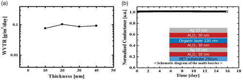
(b) shows the normalized conductance curves versus the time of metal-containing TFE. As the Ca layer was oxidized by the water vapor and oxygen that permeated through the TFE, the real-time resistance change of the Ca layer was converted into the normalized conductance value through comparison with the initial resistance of the Ca layer. In this way, the WVTR of the multibarrier was calculated using the slope of the graph. In the case of the 240-nm-thick multibarrier, the average WVTR was . As the WVTR of glass-lid-type encapsulation determined through the Ca test was
, the proposed Ca testing system can measure up to 10−6 g/m2/day. In the comparison of the multibarrier and glass-lid-type encapsulation, the metal-containing TFE multibarrier showed sufficiently good barrier properties for application to OLED devices.
3.2. Evaluation of the flexibility of the multibarrier
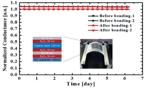
A metal-containing TFE multibarrier was fabricated using materials with good mechanical flexibility, and it was expected that a multibarrier with high resistance to bending stress would be achieved. To clearly show that the Ag thin film is effective for flexibility, the flexibility improvement was first evaluated according to the existence of an Ag thin film prior to the fabrication of the multibarrier. Only a rigid 30-nm-thick Al2O3 layer was deposited on a PET substrate three times in a row. Also fabricated was an Al2O3/Ag 2.5-dyad multibarrier with two Ag layers. shows the change in the WVTR values of the two samples according to the bending. As the result of the Ca test, the multilayer with an Ag thin film had much better bending stress owing to the good mechanical flexibility of Ag. Based on this result, the flexibility of the proposed multibarrier was evaluated by comparing the change in the WVTR after bending with tensile stress, as shown in . After 500 bending iterations with a bending radius of 5 cm, the WVTR was measured. As shown in , there was no degradation of the barrier properties. On the contrary, the multibarrier on which the bending test was conducted showed slightly better barrier properties. In other words, it can be said that the multibarrier maintained its barrier performance even after bending.
Figure 2. Ca test results after the bending test; comparison of the WVTR values according to the existence of Ag thin films. A tensile stress with 100 bending repetitions and with a bending radius of 4.5 cm was applied to each multilayer.
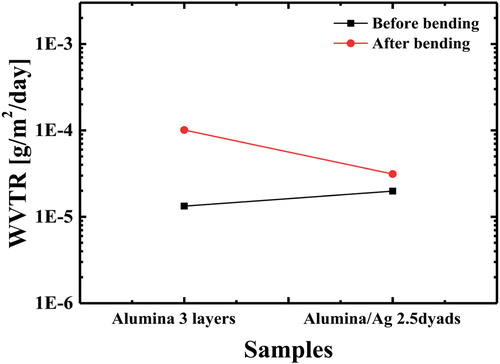
Figure 3. WVTR measurement results of the multibarrier before and after the bending test.
3.3. Thermal properties of the metal-containing TFE multibarrier for OLEDs
Finally, the heat conduction ability of the proposed TFE multibarrier was checked. To measure the performance as a heat sink, an ITO electrode was used as a heat source prior to application to OLED devices. After the formation of three distinct multibarriers on the ITO electrode for a clear comparison, the temperature difference was analyzed using an IR camera (SC-5000, FLIR).
Thermal imaging measurement was strictly done by applying identical power and surface focusing, and an identical distance between the sample and the camera. The IR camera focused on the glass surfaces of the samples for identical emissivity. In like manner, an attempt was made to minimize the measurement errors, by applying the same conditions.
Before obtaining the results, the difference between the thermal performances can be cleverly guessed by taking into account the thermal conductivity of each layer, as shown in . The previous TFE was composed of alternating organic/inorganic materials with low thermal conductivity, which degrade the heat transfer property and can result in the performance degradation of OLED devices. On the contrary, the metal-containing TFE multibarrier contains several metal layers with high thermal conductivity, and metal layers function as a heat sink due to the excellent heat conduction of metal. The study results showed the expected tendency, but the temperature difference between the samples was minor. shows that the TFE multibarrier with metal layers had a slightly better heat transfer property than the inorganic/organic multibarrier. The presence of metal layers with high thermal conductivity resulted in a small surface temperature reduction of approximately 6°C. It is guessed that the heat dissipation performance slightly improves because the ultra-thin Ag film has low thermal conductivity compared to the bulk Ag due to the size effect of nanoscale thin films [Citation18,Citation19]. Issues associated with sample size could have arisen in the measurements in this study. Large samples compared with the general pixel size of OLED devices were made for measurement purposes. Hereafter, there was a need to optimize the materials and the structure of encapsulation to improve the heat transfer performance, and thermal imaging measurement will be progressed through application to small OLED devices with the optimized encapsulation ().
Figure 4. Thermal image of the backside of the glass substrate with three different encapsulations on ITO.
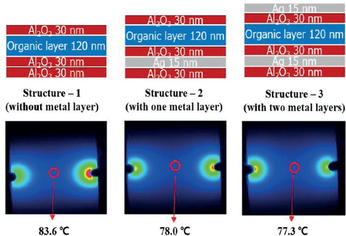
Table 1. Reported literature value of materials.
4. Summary
A sub-240-nm-thick TFE multibarrier was fabricated using Al2O3 deposited through an ALD system, spin-coated silica-nanoparticle-embedded sol-gel organic/inorganic hybrid nanocomposite (S-H) nanocomposite, and silver (Ag) deposited through thermal evaporation. The thermal and barrier properties of the metal-containing TFE multibarrier for OLEDs were investigated. The multibarrier had a high barrier performance of , which is sufficient for passivation to protect OLEDs from oxygen and water. Furthermore, the multibarrier showed good flexibility when the WVTR values before and after a bending test were compared. Finally, the metal-containing TFE multibarrier as a heat sink had a slight heat dissipation effect of Joule heating generated from the OLED, and this is a major advantage over the previous TFE multibarrier. Several experimental studies provide a solution to flexible-display encapsulation in terms of the barrier, flexibility, and heat transfer properties. In the future, a series of follow-up studies will be conducted to reliably back up the claim made herein.
Acknowledgements
The authors wish to thank Jae-Eun Pi, a researcher at the Electronics and Telecommunications Research Institute, for his help with the Mocon measurement.
Additional information
Funding
Jeong Hyun Kwon received his B.S. degree from Hanyang University in 2013, and his M.S. degree from KAIST in 2015. He is currently a Ph.D. candidate in the same institute. His research interest is thin-film encapsulation for flexible and transparent OLEDs.
Eungtaek Kim received his B.S. in Electrical Engineering degree from KAIST, Daejeon, South Korea in 2011, where he is currently working towards a Ph.D. in Electric Engineering degree. His research interests include OLED and oxide TFT passivation.
Hyeon-Gyun Im received his B.S. degree from Yonsei University in 2011, and his M.S. degree from KAIST in 2013. He is currently a Ph.D. candidate in the same institute. His research interests include inorganic/organic hybrid moisture barriers and nanowires.
Byeong-Soo Bae is a professor in the Department of Materials Science and Engineering at KAIST. He obtained his B.S. degree from Seoul National University in South Korea, and his M.Eng. and Ph.D. degrees from Drexel University and University of Arizona in the USA. Since he joined the KAIST faculty in 1994, he served as Director of the Sol-Gel Innovation Project, which is a national research program. He has been working on sol-gel-synthesized siloxane hybrid materials (hybrimers) for optics and display applications. Also, he is interested in sol-gel-based solution-processed oxide TFTs for display applications.
Ki Soo Chang received his B.S. in Electronic Materials and Device Engineering degree from Inha University in 1999, and his M.S. and Ph.D. in Information and Communications degrees from GIST in 2002 and 2007, respectively. He joined Korea Basic Science Institute in 2007, where he is presently a principal researcher of the Center for Analytical Instrumentation Development. His current research interests include the thermal imaging microscope for semiconductor device applications and the nanobiophotonic imaging system for biomedical applications.
Sang-Hee Ko Park received her B.S. and M.S. degrees from the Chemistry Education Department of Seoul National University in 1987 and 1989, and her Ph.D. degree from the Chemistry Department of the University of Pittsburgh in 1997. After graduation, she joined Electronics and Telecommunications Research Institute, South Korea in 1998, where she worked on the fabrication of electroluminescent displays. She has been working on the passivation of OLEDs and material development for flat panel displays. Since 2005, she has been working on oxide TFTs for application to AMOLEDs, flexible AMOLEDs, TFT-LCDs, and transparent displays. Since March 2014, she has been a professor at the Department of Material Science and Engineering in KAIST.
Kyung Cheol Choi received his Ph.D. degree from Seoul National University in 1993. He is currently a professor at the School of Electrical Engineering, KAIST, Daejeon, South Korea.
References
- S.F. Lim, W. Wang, and S.J. Chua, Mater. Sci. Eng., B. 85, 154 (2001). doi: 10.1016/S0921-5107(01)00599-2
- S. Gardonio, L. Gregoratti, P. Melpignano, L. Aballe, V. Biondo, R. Zamboni, M. Murgia, S. Caria, and M. Kiskinova, Org. Electron. 8, 37 (2007). doi: 10.1016/j.orgel.2006.10.005
- J.D. Affinito, M.E. Gross, C.A. Coronado, G.L. Graff, I.N. Greenwell, P.M. Martin, Thin Solid Films. 290–291, 63 (1996). doi: 10.1016/S0040-6090(96)09202-4
- L.L. Moro, T.A. Krajewski, N.M. Rutherford, O. Philips, R.J. Visser, M.E. Gross, W.D. Bennett, and G.L. Graff, presented at the SPIE on organic light-emitting materials and devices, San Diego, 2004.
- Y.C. Han, K.H. Jung, K.C. Choi, and B.S. Bae, Org. Electron. 12, 609 (2011). doi: 10.1016/j.orgel.2011.01.007
- W.H. Kim, S. Kwon, S.-M. Lee, J. Kim, Y.C. Han, E.T. Kim, and K.C. Choi, Org. Electron. 14, 3007 (2013). doi: 10.1016/j.orgel.2013.09.001
- J. Lewis, Mater. Today. 9, 38 (2006). doi: 10.1016/S1369-7021(06)71446-8
- Y.C. Han, E.T. Kim, and K.C. Choi, Org. Electron. 14, 1435 (2013). doi: 10.1016/j.orgel.2013.03.008
- E.T. Kim, Y.C. Han, W.H. Kim, K.C. Choi, H.-G. Im, and B.-S. Bae, Org. Electron. 14, 1737 (2013). doi: 10.1016/j.orgel.2013.04.011
- S.H. Kim, C. Jang, K.J. Kim, S.I. Ahn, and K.C. Choi, IEEE Trans. Electron. Dev. 57, 3370 (2010). doi: 10.1109/TED.2010.2076812
- C. Jang, E.T. Kim, and K.C. Choi, J. Disp. Technol. 8, 250 (2012). doi: 10.1109/JDT.2011.2177242
- J.W. Park, H.K. Ham, and C.Y. Park, Org. Electron. 12, 227 (2011). doi: 10.1016/j.orgel.2010.11.023
- J.H. Kwon, E.T. Kim, S.H. Ko-Park, and K.C. Choi, IMID 2014 Technical Digest. 270 (2014).
- J.H. Jin, J.J. Lee, and B.-S. Bae, Org. Electron. 13, 53 (2012). doi: 10.1016/j.orgel.2011.09.008
- R. Paetzold, A. Winnacker, D. Henseler, V. Cesari, and K. Heuser, Rev. Sci. Instrum. 74, 5147 (2003). doi: 10.1063/1.1626015
- J.T. Felts, J. Plast. Film Sheet. 9, 139 (1993). doi: 10.1177/875608799300900206
- J. Sun, W.S. Lai, and H. Gong, J. Appl. Phys. 111, 083712 (2012). doi: 10.1063/1.4704686
- F. Voelklein and T. Franke, presented at the 23rd International Thermal Conductivity Conference (ITCC), Nashville, 1996 (published).
- C. Yip-wah, Master's thesis, Heat conduction in polycrystalline metal films, University of Hong Kong, 1973.