
Abstract
Reported in this work is the fabrication of white transparent organic light-emitting diodes (TOLEDs) with high color rendering indices (CRIs). An architecture in which the green and red emission layers are sandwiched between two blue emissions layers was used. By tuning the thicknesses of the green and red emission layers, CRI and power efficiency values of 90/20.5 and 87/6.8 lm/W were achieved in the bottom and top emissions, respectively. The study results suggest an effective engineering approach for realizing high CRI white TOLED lighting sources.
1. Introduction
The compelling need for human-friendly, energy-efficient, and environmentally sound lighting sources can be answered by organic light-emitting diodes (OLEDs). OLEDs are electroluminance (EL)-type devices, in which light emission takes place through electron-hole recombination. They are environmentally sound light sources that do not produce excessive heat and do not contain toxic materials. OLED itself is ultra-thin (<200 nm) and has very low weight, and can be tailored in many formats [Citation1–6]. For example, OLEDs with flexible physical features enable the use of OLED luminaries in curved surfaces without giving rise to space occupation and heavy weight concerns. Also, as OLED light is ultra-violet (UV)-free, it can be used to illuminate human and biological substances without producing harmful effects. The light of OLEDs is also diffusive and soft and is thus human-friendly and comfortable, offering a preferable light quality for interior lighting.
Uniquely, OLED can be engineered to be a transparent bidirectional light source. Transparent OLED (TOLED) refers to a bidirectional OLED that emits light from its top and bottom surfaces [Citation7–9]. TOLEDs can be used to fabricate architectural luminary windows and see-through displays. TOLED components, however, must bear optical transparency. In the conventional bottom-emission-type OLEDs, the device components are usually optically transparent. The metallic cathode, however, is opaque. To achieve an optically transparent cathode, the thick (>100 nm) metallic cathode is replaced with thin Ag films, which offer low sheet resistance and low absorption [Citation10,Citation11].
In this work, white TOLEDs with high color rendering indices (CRIs) in the top and bottom emissions are presented. The CRI may be defined as the closeness to the spectrum of sunlight [Citation12–15]. A CRI of 100, an ideal number for white light, indicates exact spectral matching to sunlight. White light with a high CRI not only reveals the true colors of objects but also has a soothing effect due to its similarity to natural light. Due to the existing optical asymmetry in the TOLEDs, it is technically difficult to achieve high CRI values in the bottom and top emissions [Citation16–18]. As white light is a composite of many lights, the task of achieving a high CRI in both emission directions is challenging. Especially, it is important to stabilize the blue spectrum, which is the weak portion of OLEDs. To overcome this obstacle, a TOLED device architecture in which the red and green emission layers are sandwiched between two blue emission layers is suggested. To modulate the CRI values, the thicknesses of the green and red emission layers were varied. Such approach obviates the need for changing the organics or varying the dopant concentration, allowing a rather straightforward way of tuning the CRI values of TOLEDs.
2. Experiments
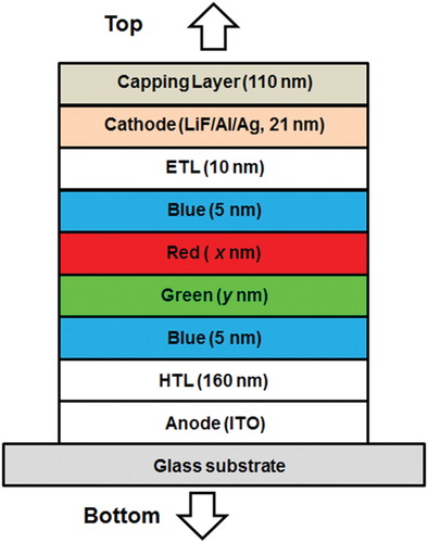
(a) shows the cross-sectional schematics of the proposed white TOLED. A vacuum thermal deposition method was used to form the TOLED. The base pressures of all the deposition processes were below 6.66 × 10⁻⁵ Pa. A 0.7-mm-thick glass substrate was used. The emission area was 2 × 2 mm. The phosphorescent three-color-type OLED was adopted to produce white light. The red and green emission layers were positioned between the blue emission layers. The anode- and cathode-side blue layers were TCTA:Firpic (5 nm: 7%) and DCzppy:Firpic (5 nm: 10%). TCTA and DCzppy refer to 4,4′,4′′-tris(N-carbazolyl)-triphenylamine and 2,6-bis(3-(carbazol-9-yl)phenyl) pyridine, respectively. The host material TCTA and DCzppy were intentionally chosen to match the charge type of the adjacent electrode. This architecture was chosen to augment and stabilize the blue portion of white light. The thicknesses of the upper and lower blue emission layers were both fixed at 5 nm. To modulate the CRI of the top and bottom emissions, the thicknesses of the green and red emission layers were varied (thickness of red layer: 0.6, 0.8, 1.0, and 1.2 nm; thickness of green layer: 0.8, 1.0, and 1.2 nm). LiF(1 nm)/Al(1.5 nm)/Ag(20 nm) was used as the transparent cathode. The technical background of the choice of this transparent format has been described elsewhere [Citation9,Citation10,Citation17]. Briefly, LiF facilitates electron injection, and Al suppresses the formation of a highly granular Ag film. On the top of the transparent cathode, a 110-nm-thick 1,1-bis[(di-4-tolylamino)phenyl]cyclohexane (TAPC) organic capping layer (CL) was formed. CL is an optical layer that is useful in tuning the efficiency and transmittance of TOLEDs. The CL thickness can be varied to induce either a constructive or a destructive interference in the internal optics of the TOLED [Citation17,Citation18]. To electrically stabilize the device, the hole transport layer (HTL) was designed to have an alternating sequence of Hat-CN (10 nm) and TAPC (45 nm). A total of three pairs of Hat-CN(n-type)/TAPC(p-type) were used as the HTL. Hat-Cn refers to 1,4,5,8,9,11-hexaazatriphenylene hexacarbonitrile. The details of this HTL have been described elsewhere [Citation9]. For ETL, 10-nm-thick 1,3-bis(3,5-di-pyrid-3-yl-phenyl)benzene (BmPyPB) was used. The anode was 70-nm-thick indium tin oxide. The fabricated TOLED devices were immediately glass-encapsulated in an inert glove box environment. UV-curable epoxy resin was used to glue the glass, and a getter was included to collect moisture. The EL spectra were collected using a spectroradiometer (CS-200, Minolta). The current density(J)–voltage(V)–luminance(L) characteristics were obtained using sourcemeasure units (Keithley 238) and the aforementioned spectroradiometer. The transmittance of the glass-encapsulated TOLED was measured using a UV-visible spectrophotometer (U-3501, Hitachi). The surface morphologies of the cathode films were investigated through scanning electron microscopy (SEM, Model: Sirion 400, Philips).
Figure 1. Architecture of the white TOLED.
3. Results and discussion
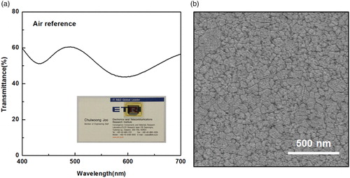
(a) shows the measured transmittance of the proposed TOLED in the visible range. The average transmittance is 53%. The transmittance oscillates slowly and becomes lower as the wavelength increases. The inset shows an actual image of the proposed TOLED placed on a namecard. The letter “R” is readily discernable, without blur. (b) shows the SEM image of the Ag surface. The surface is not totally smooth but is slightly granular. The domains, however, are not disconnected entities but contact one another to provide percolation paths. The domain size ranges from 50 to 150 nm. The formation of a granular structure is due to the wetting in relation to the Al layer underneath, on which the Ag layer was deposited. Technically, it is important to choose a material that bears wettability to Ag. Otherwise, a highly granular Ag structure will develop, leading to high sheet resistance and low transmittance [Citation11,Citation12].
Figure 2. (a) Measured transmittance of TOLED. (b) SEM image of an Ag surface.
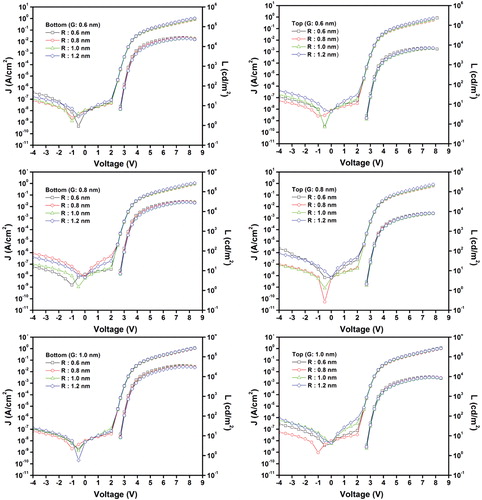
summarizes the J–V–L characteristics of the proposed TOLED. The variations in the thicknesses of the red and green emission layers do not significantly alter the J–V characteristics. The J–V lines are almost superimposed in the voltage range higher than 0 V. The J level increases rapidly up to approximately 5 × 10⁻² A/cm2, and is gradually saturated. The J level does not exceed 10−6 A/cm2 under reverse bias conditions, signaling the usefulness of the proposed Hat-CN/TAPCHTL structure. In all the cases, 103 cd/m2 L was achieved at a 3.5 V applied voltage, indicating facile and stable charge transport across the device structure. The Ls of the bottom emission are higher than those of the top emission due to the asymmetric internal optics and CL thickness. The CL thickness can be varied to either increase the total transmittance or enhance the total efficiency [Citation17,Citation18]. To achieve high total efficiency, 110 nm CL thickness was chosen, at which the reflection toward the bottom side is high. The reflective optical component can constructively couple with the bottom-direction traveling light to enhance the luminance. The highest achieved L was approximately 5 × 10⁴ cd/m2 in the bottom emission.
Figure 3. J–V–L characteristics of the bottom and top emissions as functions of the red and green emission layer thicknesses.
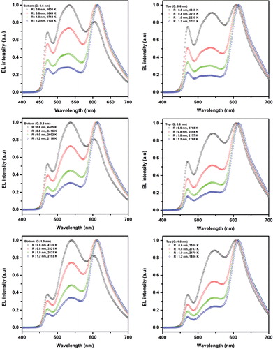
shows the normalized bottom and top EL spectra of the proposed white TOLEDs. As expected, increasing the thickness of either the red or green emission layer enhances the intensity of the corresponding color. The relative intensity increases, and the width at half maximum narrows. These effects are more pronounced in the green emission layer than in the red emission layer. The change in the thickness of the layer causes the physical repositioning of the recombination zone [Citation12,Citation13]. As a result of the repositioning of the recombination zone, the internal optical length and microcavity change, inducing peak shifts. These were observed as the main peak shifts toward a higher wavelength. The relative intensity enhancement due to the thickness increase was observed to be bigger in the green emission layer than in the red emission layer. The factors behind this observation imply a difference in charge transport and/or the possibility of developing a confined recombination zone [Citation12,Citation13]. The relative intensities ratio of blue to red was observed to be stable, removing the complexity involved in modulating CRIs. The changes in the relative intensities of red, green, and blue demonstrate the technical possibility of modulating the CRI values of the bottom and top emissions.
Figure 4. EL spectra of the bottom and top emissions as functions of the red and green emission layer thicknesses.
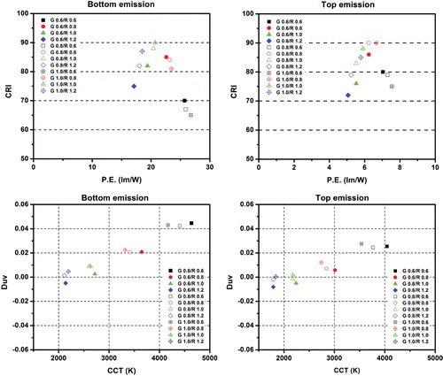
To relate the power efficiencies (PEs) and CRI values, relevant values were extracted using Figures and . (a) and 5(b) show the CRI and PE values as functions of the thicknesses of the green and red emission layers. The values were obtained at a constant J of 2 mA/cm2. PE was chosen as the efficiency measure because it allows not only the spectral characteristics but also the electrical power consumption to be considered. Both are important in assessing the performance of white OLEDs for lighting purposes. In the bottom-emission case, the CRI values tended to become lower as the PE became higher. A similar trend was observed in the top emission, but such correlation was not as obvious as in the bottom emission case. The PE of the bottom emission was higher by approximately a factor of three. The PE of the top emission was lower due to the optical engineering of the CL, the absorption at the Ag, and the glass encapsulation. The optical loss due to the glass encapsulation was reported to be approximately 10% [Citation10]. At the 1.0 nm green and red thicknesses, the highest PEs that were obtained in the bottom and top emissions were 20.5 and 6.8 lm/W, respectively. Coincidentally, the highest PE coincided with the highest CRI values. The corresponding CRI values for the bottom and top emissions were 90 and 87, respectively. These CRI values qualify for the light source for indoor lighting. The PEs of bottom-emission-type OLEDs with very high CRI values (>90) do not exceed 10 lm/W. The majority of CRI values lie within the range of 77–87, with a PE of approximately 25 lm/W [Citation12,Citation14]. (c) and 5(d) show the Duv and correlated color temperature (CCT) of the proposed TOLEDs. Generally, the CCT is low when the white emission is reddish, and high when the white emission is bluish. Duv is defined as the distance away from the Planckian locus in the 1960 chromaticity diagram. The method described by Ohno was used to extract the Duv values. This method is documented elsewhere [Citation19]. For the given thicknesses of the red and green emission layers, the top emissions showed lower CCT values than their counterparts. The results in show that the relative EL intensities of the red portion were stronger in the top emission, resulting in a lower CCT. The Duv and CCT values were observed to increase proportionally. In the red augmented samples, whose red emission layer thicknesses were either 1.0 or 1.2 nm, the Duv fell within ±0.01. In the green augmented samples, bigger Duv values were observed. Technically, these results imply the importance of controlling the green emission intensity to lower the deviation away from the Planckian locus, and to maintain high-quality white light.
Figure 5. CRI and PE values of the (a) bottom emission and (b) top emissions as functions of the red and green emission layer thicknesses. DuV and CCT values of the (c) bottom emission and (d) top emissions as functions of the red and green emission layer thicknesses.
To achieve both a high CRI and a high PE in TOLEDs, at least three factors must be considered: the charge transport, the positioning of the recombination zone, and the modulation of the transmittance. As such, the architecture of the TOLED is of prime interest. The results of this study show that adopting a CL-equipped TOLED architecture, in which the green and red emission layers are sandwiched between two blue emission layers, makes it possible to achieve both a high CRI and a high PE in both directions. Placing the blue emission layers close to the electrode with charge polarity matching made it possible to stabilize the blue. These give design freedom in choosing the thicknesses of the green and red emission layers and in addressing the objectivity of a high CRI and a high PE in the bottom and top emission directions.
4. Summary
In summary, white transparent organic light-emitting diodes (TOLEDs) with high CRI values were fabricated in the bottom and top emissions. The proposed CL-equipped TOLEDs have an emission layer structure in which the green and red emission layers are situated between two blue emission layers. The CCT values were tuned by varying the thicknesses of the green and red emission layers. The variations in the green and red emission layer thicknesses induced noticeable changes in the EL spectra and a marginal change in the electrical characteristic. The optimized TOLED can achieve high CRI values of 90 at a CCT of 2631 K, and 87 at a CCT of 2180 K, in the bottom and top emissions, respectively. The results of this study present a facile yet straightforward method of producing warm white light in TOLEDs. Also, the proposed approach can be readily used for the fabrication of OLED luminescent devices to produce a great variety of lighting environments.
Acknowledgement
This work was financially supported by the Development of a Key Technology for Interactive Smart OLED Lighting ITR&D program, which is a part of the ETRI Internal Research Fund from the South Korean Ministry of Science, ICT, and Future Planning.
Additional information
Chul Woong Joo received his B.S. and M.S. in Polymer Science and Engineering of Organic Electronics Devices degrees from Dankook University, Cheonan, South Korea in 2008 and 2010, respectively. He joined the Electronics and Telecommunications Research Institute in Daejeon, South Korea in 2011, and his current research interests include device architectures in OLEDs and next-generation displays.
Jaehyun Moon received his B.S. in Metal Engineering degree from Korea University, Seoul, South Korea in 1995, and his Ph.D. in Materials Science and Engineering degree from Carnegie Mellon University, Pittsburgh, PA, USA in 2003. From 2003 to 2004, he was a postdoctoral associate at the Max-Planck Institute, Stuttgart, Germany. He joined the Electronics and Telecommunications Research Institute in Daejeon, South Korea in 2004. His current research interests include flexible electronics, functional nanomaterials, and OLEDs.
Jun-Han Han received his B.S. and M.S. in Electronic Engineering degrees from Hanyang University, Seoul, South Korea in 2007 and 2009, respectively. He joined the Electronics and Telecommunications Research Institute in Daejeon, South Korea in 2009 and continues to research on OLED lighting applications and next-generation displays.
Jin Woo Huh worked for the Institute of Advanced Engineering and Orion Electric Co., Ltd. after receiving her M.S. in Physics degree from Ehwa Women's University in Seoul, South Korea in 1995. Then she earned her Ph.D. in Electrical Engineering degree from Korea University in Seoul, South Korea in 2010. Thereafter, she joined the OLED lighting team at the Electronics and Telecommunications Research Institute in Daejeon, South Korea. Her current research interests include transparent OLEDs and light extraction techniques.
Jin-Wook Shin received his B.S. in Electronic Engineering degree from Myongji University in Yongin, South Korea in 2007, and his M.S. in Electronic Materials Engineering degree from Kwangwoon University in Seoul, South Korea in 2009. He joined the Electronics and Telecommunications Research Institute in Daejeon, South Korea in 2009. His current research interests include light extraction technologies for OLEDs.
Doo-Hee Cho received his Ph.D. in Materials Chemistry degree from Kyoto University in Kyoto, Japan in 1996. He worked in the areas of float glass and low-e coating at KCC Corp., Seoul, South Korea from 1996 to 1998. Since he joined the Electronics and Telecommunications Research Institute in Daejeon, South Korea in 1998, he has been involved in specialty optical fiber, transparent oxide TFT, and OLED lighting research. His major research interests include the optical structure and light extraction of OLEDs. Since 2009, he has been working on the international standardization for OLED lighting as a member of IEC TC34.
Jonghee Lee received his B.S., M.S., and Ph.D. in Chemistry degrees from the Korea Advanced Institute of Science and Technology in Daejeon, South Korea in 2002, 2004, and 2007, respectively. He joined the Electronics and Telecommunications Research Institute in Daejeon, South Korea in 2007, and worked on white OLEDs for display and lighting applications. He then moved to the Institut für Angewandte Photophysik (IAPP, Prof. Karl Leo's group) at the Technische Universitat in Dresden, Germany in 2010, as a postdoctoral associate. After two years, he joined ETRI again. He has been working on new-concept display modes as well as light extraction techniques for OLEDs.
Nam Sung Cho received his B.S. in Chemistry degree from Chung-Ang University in Seoul, South Korea in 2000, and his M.S. and Ph.D. in Chemistry degrees from the Korea Advanced Institute of Science and Technology in Daejeon, South Korea in 2002 and 2006, respectively. From 2006 to 2008, he was a postdoctoral associate at the University of California Santa Barbara in Santa Barbara, CA, USA. From 2008 to 2012, he worked on materials development for OLEDs at LG Display R&D Center in Paju, South Korea. He joined the Electronics and Telecommunications Research Institute in Daejeon, South Korea in 2012. His current research interests include OLED structures, OLED materials, and white OLEDs.
Jeong-Ik Lee received his B.S., M.S., and Ph.D. in Chemistry degrees from the Korea Advanced Institute of Science and Technology in Daejeon, South Korea in 1992, 1994, and 1997, respectively. After graduating, he joined IBM Almaden Research Center in San Jose, CA, USA as a postdoctoral associate, and worked on organic light-emitting materials. He moved to the Electronics and Telecommunications Research Institute in Daejeon, South Korea in 1999 and continued his research on organic light-emitting materials and devices.
References
- C.W. Tang and S.A. Vanslyke, Appl. Phys. Lett. 51, 913 (1987). doi: 10.1063/1.98799
- M.A. Baldo, D.F. O'Brien, Y. You, S. Shoustikov, M. Sibley, E. Thompson, and S.R. Forrest, Nature. 395, 151 (1998). doi: 10.1038/25954
- B.W. D'Andrade and S.R. Forrest, Adv. Mater. 16, 1585 (2004). doi: 10.1002/adma.200400684
- Y. Sun, N.C. Giebink, H. Kanno, B. Ma, M.E. Thompson, and S.R. Forrest, Nature. 440, 908 (2006). doi: 10.1038/nature04645
- D.-H. Cho, J.-W. Shin, J. Moon, S.K. Park, C.W. Joo, N.S. Cho, J.W. Huh, J.-H. Han, J. Lee, H.Y. Chu, and J.-I. Lee, ETRI J. 36 (5), 847 (2014). doi: 10.4218/etrij.14.0113.0845
- J.-W. Lee, J. Lee, H.Y. Chu, and J.I. Lee, J. Inform. Display. 14, 57 (2013). doi: 10.1080/15980316.2013.783512
- V. Bulvoic, G. Gu, P.E. Burrow, M.E. Thomson, and S.R. Forrest, Nature. 380, 29 (1996). doi: 10.1038/380029a0
- J. Moon, J.W. Huh, C.W. Joo, J.-H. Han, J. Lee, H.Y. Chu, and J.-I. Lee, SPIE Newsroom, (November 2013). doi:10.1117/2.1201310.005197
- C.W. Joo, J. Moon, J.-H. Han, J.W. Huh, J. Lee, N.S. Cho, J. Hwang, H.Y. Chu, and J.-I. Lee, Org. Electron. 15, 189 (2014). doi: 10.1016/j.orgel.2013.10.005
- J.W. Huh, J. Moon, J.W. Lee, J. Lee, D.-H. Cho, J.-W. Shin, J.-H. Han, J. Hwang, C.W. Joo, J.-I. Lee, and H.Y. Chu, Org. Electron. 14, 2039 (2013). doi: 10.1016/j.orgel.2013.04.035
- G.W. Kim, R. Lampande, J. Boizot, G.H. Kim, D.C. Choe, and J.H. Kwon, Nanoscale. 6, 3810 (2014). doi: 10.1039/c3nr05861a
- Y. Li, K. Xu, X. Wen, L. Zhang, Y. Yin, S. Liu, X. Piao, and W. Xie, Org. Elec. 14, 1946 (2013). doi: 10.1016/j.orgel.2013.04.027
- J.-H. Jou, S.-M. Shen, C.-R. Lin, Y.-S. Wang, Y.-C. Chou, S.-Z. Chen, and Y.-C. Jou, Org. Elec. 12, 865 (2011). doi: 10.1016/j.orgel.2011.02.012
- C.-C. Fan, M.-H. Huang, W.-C. Lin, H.-W. Lin, Y. Chi, H.-F. Meng, T.-C. Chao, and M.-R. Tseng, Org. Elec. 15, 517 (2014). doi: 10.1016/j.orgel.2013.11.040
- Y.H. Son, S.H. Kim, and J.H. Kwon, J. Inform. Display. 15 (4), 185 (2014). doi: 10.1080/15980316.2014.963715
- W. Ji, J. Zhao, Z. Sun, and W. Xie, Org. Electron. 12, 1137 (2011). doi: 10.1016/j.orgel.2011.03.042
- J.W. Huh, J. Moon, J.W. Lee, D.-H. Cho, J.-W. Shin, J.-H. Han, J. Hwang, C.W. Joo, J.-I. Lee, and H.Y. Chu, IEEE Photonics Soc. 4, 39 (2012). doi: 10.1109/JPHOT.2011.2176478
- J.W. Huh, J. Moon, J.W. Lee, D.-H. Cho, J.-W. Shin, J.-H. Han, J. Hwang, C.W. Joo, H.Y. Chu, and J.-I. Lee, Org. Electron. 13, 1386 (2012). doi: 10.1016/j.orgel.2012.04.005
- Y. Ohno, LEUKOS 10, 47 (2014). doi: 10.1080/15502724.2014.839020