
Abstract
In this study, we investigated the use of biomaterials in optoelectronic applications. One of the most abundant biomaterials in nature is deoxyribonucleic acid (DNA). It was used in this study as an alignment layer to fabricate a twisted-nematic-mode (TN-mode) liquid crystal display (LCD). To create the LCD, a cheap DNA material extracted from salmon was used to coat an indium tin oxide glass substrate, and the DNA chains were aligned with a simple but effective mechanical shearing method at room temperature. Then small rod-type LC molecules were spread on top of the alignment layer, obliquely aligned with respect to the long axis of the DNA chains because of the polar and topographical interactions between the LC molecules and the DNA material. The electro-optical characteristics of the LCD device were examined to compare the properties of the DNA-based LCD with those of a TN-mode LCD fabricated with the conventional rubbed polymer alignment layer. We believe our method provides an easy and useful tool for the fabrication of biomaterial-based optoelectronic devices.
1. Introduction
Deoxyribonucleic acid (DNA) is a readily available and abundant biomolecule in nature that has been widely used in biosensing applications [Citation1–6]. Beyond this mature application, there has been increasing interest in using DNA as a dielectric material or a semiconductor in optoelectronic devices [Citation7–9], as well as for templating applications to guide guest materials, such as particles, biopolymers, and liquid crystals (LCs), because of its fine structure [Citation10–16]. DNA chains have topographic grooves and ridges because of their double helical structure and the rich supply of negative charges on their surface that interact with various nanomaterials. Despite these merits, the use of DNA has been limited in optoelectronic applications because of the high costs of the required synthetic and purification processes [Citation17]. Recently, a number of simple and inexpensive methods of extracting DNA have been introduced [Citation18,Citation19]. A large amount of DNA can be extracted from fish waste, such as salmon milt and roe, after which the impurities and unusable proteins are removed, with the DNA freeze-dried to make a raw DNA powder. However, this natural DNA is insoluble in organic solvents, which makes it difficult to use in optoelectronic applications. To overcome this problem, an acationic surfactant, such as cetyl trimethyl ammonium, is added to form a DNA-cationic complex that is soluble in organic solvents, which allows DNA to be readily used in many optoelectronic applications [Citation20].
While these crude DNA materials have a large distribution of dimensions that range from approximately 75 to 4000 nm, which corresponds to 200–12,000 base pairs, the typical intrinsic dimensions are fixed at 3.4 Å between the base pairs and are approximately 2.2 nm in diameter. In addition, while the sequence of the base pairs cannot be controlled with this method, the topographic characteristics of the DNA are enough to control the ordering and orientation of functional materials in practical applications [Citation13,Citation14].
Of the various kinds of functional materials, LCs are good candidates for what? Because they have a facile response to interfacial forces due to their liquid-like fluidity and structural anisotropy [Citation12,Citation21]. To use DNA in template applications, the DNA chains should be uniformly aligned in a certain direction on the electrodes of a glass or silicon wafer. There are many methods of obtaining such well-ordered DNA structures, such as molecular combing [Citation22], magnetic fields [Citation23], shear forces [Citation12], and topographic confinement [Citation24,Citation25]. However, these conventional methods require large experimental setups and are high-cost and time-consuming processes, which must be overcome so that DNA films could be used as a practical alignment layer in LC devices.
In this study, we successfully fabricated a twisted-nematic-mode (TN-mode) LC display (LCD) with a shear-aligned DNA film. To fabricate this device, a simple brushing method was developed that allowed us to achieve highly aligned DNA films over a large area [Citation26]. This method has several advantages over the conventional alignment processes because it is a one-step process that is performed in only a few minutes and can be implemented at room temperature [Citation27]. In addition, the electro-optical (EO) properties of our device are comparable to those of the conventionally fabricated LCDs. Thus, the application in this study of DNA as an alignment layer should encourage the use of other abundant and cheap biomaterials in optoelectronic applications in the future.
2. Results and discussion
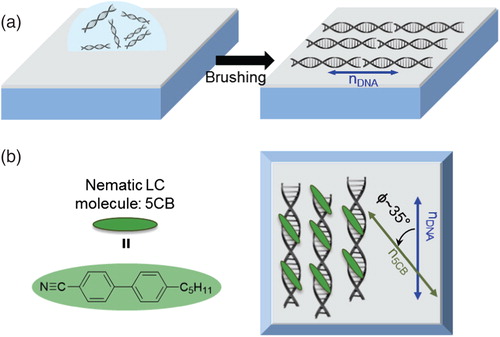
The synthetic procedure used to fabricate the LCD device is summarized in . To fabricate the TN-mode LCD with a DNA alignment layer, transparent electrode substrates were prepared by depositing indium tin oxide (ITO) on glass wafers. Then the double-strained DNA (dsDNA) solution (DNA dissolved in water, concentration = 20 wt%) was spread on the substrates and sheared in one direction with a commercially available makeup brush (Olive Young Shadow Brush, Korea) to produce a DNA film with uni-axially aligned chains (the direction of the chains was labeled ‘nDNA’) ((a)). After the water in the DNA film was evaporated, the two substrates were assembled to form a sandwich cell with a 3-µm gap. Then the nematic LC (NLC) material, 4-cyano-4′-pentylbiphenyl (5CB), was injected into the cell via capillary force, and the direction of the 5CB molecules (n5CB) was obliquely aligned with respect to nDNA because of the helical grooves of the dsDNA ((b)).
Figure 1. Schematic illustration of the preparation for the DNA alignment layer and well-oriented LC molecules. (a) The DNA molecules were aligned parallel to the brushing direction, resulting in the unidirectional DNA film on the ITO glass. (b) Molecular structure of the 5CB LC molecule and schematic sketches of aligned LC molecules on the brushed DNA layer.
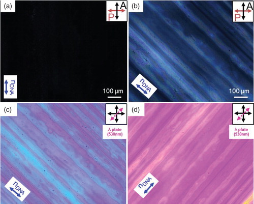
To investigate the orientation of the shear-aligned dsDNA on the substrates, depolarized transmitted light microscopy (DTLM) was performed. DNA is well known to have a negative birefringence because of its end-to-end-stacked base pairs that act as discotic molecules with an optical axis perpendicular to nDNA [Citation28]. The dark and bright domains that appear when the brushing direction is parallel ((a)) or tilted ((b)) with respect to the polarizer indicate that the dsDNA can be aligned either parallel or perpendicular to the brushing direction, respectively. To confirm the exact orientation of the dsDNA, a first-order retardation plate (λ = 530 nm) was inserted between the sample and the analyzer to observe the color changes depending on the retardation of the wavefront of the light passing through the sample. With this setup, the sample color appeared to have been magenta when the sample was isotropic or when the optical axis of the sample with birefringent characteristics was parallel to one of the polarizers in the DTLM setup. On the other hand, the sample appeared cyan or yellow when the optical axis was parallel or perpendicular to the slow axis of the retardation plate, as indicated by the dashed lines in (c) and 2(d), respectively. In our study, the cyan and yellow colors appeared when the brushing direction was perpendicular and parallel to the slow axis of the retardation plate, respectively, which indicates that the dsDNA is aligned parallel to the brushing direction ((c) and (d), respectively).
Figure 2. DTLM images of the DNA alignment layer on the ITO glass substrate. (a) DTLM image of the aligned DNA layer when the brushing direction was parallel to the analyzer and (b) at −45° with respect to the analyzer. A first-order retardation plate (λ = 530 nm) was inserted to investigate the direction of the DNA. (c) DTLM images of the sample when the brushing direction was at −45° and at (d) +45° with respect to the polarizer.
The TN-mode cell was fabricated using two DNA-coated substrates with 3-µm-thick ballspacers. Then the 5CB molecules were injected into the cell at approximately 40°C, which is the isotropic temperature of 5CB. When nDNA is parallel to the analyzer or the polarizer, the cell exhibits high light transmission, as shown in (a). On the contrary, the cell exhibits good extinction when nDNA is rotated by approximately 35° with respect to the analyzer ((b)) because the azimuthal angle (φ) between the LCs (n5CB) and the DNA chains (nDNA) is approximately 35° ((b)). The irregular white lines in (b) were caused by the birefringence of the underlying DNA alignment layer, which slightly affected the white level of the device because the DNA layer showed no light retardation. In addition, the typical degraded dark levels of the LCDs did not occur when the DNA layer was so thin so that the birefringence of the DNA on the substrate was not visible. For this, we will find the optimum process parameters, including the brushing force, DNA concentration, and water evaporating speed, under an appropriate humid condition.
Figure 3. DTLM images of the 5CB LC molecules on the brushed DNA alignment layer. (a) The sample exhibited high light transmission when the brushing direction was parallel to the analyzer and (b) good extinction when the brushing direction was at –35° with respect to the analyzer. The white lines are due to the non-existent light retardation of the underlying DNA layer. (c) Transmittance of the sample as a function of the rotation angle between the brushing direction and the analyzer (θ). The transmittance exhibited a periodicity of 90°.
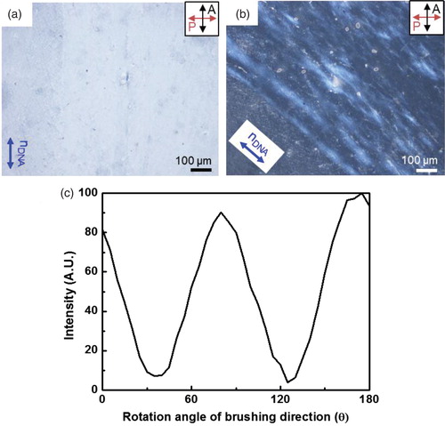
To verify the angle of the LC molecules (n5CB) with respect to the DNA chains (nDNA), the light transmittance of the sample was measured with a spectrometer (USB-2000+, Ocean Optics) and a light source (λ = 550.14 nm, SPECTRA X, Lumencor) as a function of the rotation angle between the nDNA and the analyzer. As shown in (c), the lowest transmittance intensity was measured at θ = 35°, and the highest was obtained at θ=80°. This is because the 5CB molecules were strongly anchored to the polar phosphate groups obliquely oriented with respect to the long axis of the DNA chains ((b)) [Citation12]. This indicates that the LC molecules were uniformly aligned with nDNA, i.e. that the brushed DNA layer aligned the NLCs well to fabricate the DNA-based LCD.
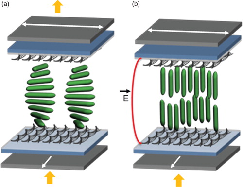
Regarding the investigation of the angle between n5CB and nDNA, a schematic of the TN-mode LC cell with a DNA layer is shown in . Our device is normally in the ‘bright mode’ ((a)) and, thus, the polarized light passing through the first polarizer is guided by the DNA-aligned 5CB LC molecules when no electric field is present [Citation29]. When the electric field (E) is applied to the cell, most of the 5CB molecules become vertically aligned parallel to E, which results in the ‘dark mode’, as shown in (b). Based on this strategy, the EO responses of the TN-mode LCD were measured as functions of the applied AC electric field with a frequency (f) of 1 kHz.
Figure 4. Schematic diagrams of the TN-mode LC cell with a DNA alignment layer. (a) Without an external electric field, the LC molecules had a twisted-nematic arrangement in the cell. Thus, the polarized light of the bottom polarizer was guided by the LCs and passed through the top polarizer, which resulted in a ‘bright mode’. (b) With an applied electric field (E), the LC molecules were realigned in the direction of E, and thus, the polarized light could not pass through the LCs, which were blocked by the top polarizer, and resulted in a ‘dark mode’. The total twisted angle was 70°.
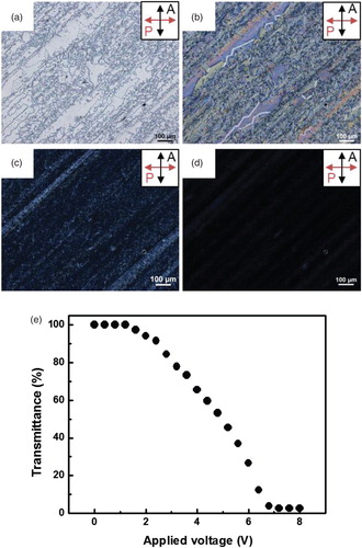
As mentioned in the preceding paragraph, our cell is normally in the bright mode, which allows light transmission when no electric field is applied to the cell. Thus, the DTLM image of the cell with no electric field present is very bright ((a)), with the optical axis of the bottom polarizer parallel to the brushing direction ((a)). The threshold voltage of the cell (Vth) is approximately 2.4 Vrms. As the applied voltage exceeds Vth, the transmittance decreases ((b–d)) because n5CB gradually aligns with E. The applied voltage–transmittance (V–T) plot for our cell showed this trend very clearly ((e)). As the applied voltage increased, the transmittance of the device gradually decreased [Citation30], which is important for grayscale LCDs. In addition, the saturation voltage was approximately 6.4 Vrms. Therefore, the driving voltage of our DNA-aligned LCD was slightly higher than that of the conventional LCDs that use a rubbed polyimide alignment layer in the TN-mode cell, because the manually applied DNA film has a relatively non-uniform thickness. An automatic system, such as a roll-to-roll coating method, would enhance the EO properties of our device, which will be very important in the use of other biomaterials in optoelectronic applications.
Figure 5. DTLM images of the TN-mode cell with a brushed DNA layer. (a) With no external electric field, the twisted-nematic mode of the LCs allowed a high level of transmission between the orthogonal polarizers. (b–d) As the applied voltage increased, the electric field caused more and more of the LC molecules to be oriented normal to the cell, which caused the extinction of the light transmission. (e) Voltage-dependent transmittance curve of the device.
3. Conclusions
In summary, the TN-mode LCD device with a DNA alignment layer was successfully fabricated, and its EO properties were investigated. The LC molecules were sufficiently aligned on the highly ordered DNA layer to be used in TN-mode LCDs. The well-aligned DNA film can be easily fabricated at room temperature, and is a rapid and convenient tool that overcomes the disadvantages of the conventional rubbed polymer alignment layer, which requires complex and high-temperature processing [Citation30]. In addition, our results will contribute to the effective use of biomaterials in various patterning applications.
4. Experiment details
4.1. Sample preparation
The DNA (received from the Chitose Institute of Science and Technology) was dissolved in deionized water to form the 20-wt% DNA solution used to fabricate the TN-mode LCD. The DNA solution was brushed over two cleaned ITO glass substrates. These two substrates were assembled with silica ball spacers to form a sandwich cell with a 3-µm-thick cell gap. After the assembly of the cell, 5CB (Sigma-Aldrich), an NLC, was injected into the cell via capillary force at its isotropic temperature (approximately 40°C).
4.2. Characterization
The optical textures of the LCD were characterized with DTLM. The transmittance of the LCs on the brushed DNA layer as a function of the rotation angle between the brushing direction and the analyzer was recorded with a USB-2000+ spectrometer (Ocean Optics) equipped with a solid-state light source (SPECTRA X, Lumencor). The EO performance was measured with a home-built setup that consisted of a halogen lamp, a function generator (33210A, Agilent), a voltage amplifier (A400, FLC Electronics), a silicon photodetector (S-025-H, Electro-optical Systems), and a lock-in amplifier (SR830, Stanford Research Systems). The AC electric field (rectangular pulses with a frequency f of 1 kHz) was applied to the cell to investigate the EO responses of our device.
Disclosure statement
No potential conflict of interest was reported by the authors.
Additional information
Funding
Yun Jeong Cha received her BS in Environment Engineering degree from the University of Seoul in South Korea in 2012. She is a PhD candidate at the Graduate School of Nanoscience and Technology of the Korea Advanced Institute of Science and Technology. Her research interest is the self-assembly behavior of biomaterials and lyotropic liquid crystals.
Min-Jun Gim received his BS (2011) and MS (2013) degrees from the Department of Chemical Engineering and the Department of Display Materials Engineering, respectively, of Kyung Hee University. He is a PhD candidate at the Graduate School of Nanoscience and Technology of the Korea Advanced Institute of Science and Technology. His research interests are chiral soft materials and photonic crystals.
Kyunghwan Oh received his BS and MS in Physics degrees from Seoul National University in 1986 and 1988, respectively. He further earned his MS in Engineering and PhD in Physics degrees from Brown University in 1991 and 1994. He has been studying guided wave optics, Fourier optics, and photonic device physics, and has published more than 160 journal articles, 220 conference papers, and 25 patents. He was a professor at the Gwangju Institute of Science and Technology from 1996 to 2006. Since 2006, he has been affiliated with the Department of Physics of Yonsei University. He is a Fellow of The Optical Society of America, an Alexander von Humboldt Research Fellow (Germany), a Chevening Scholar (UK), a JSPS Invitation Fellow (Japan), and a Tan Chin Tuan Exchange Fellow (Singapore). He has been serving the photonics community as a topical editor and an associate editor of major journals, which include Optics Letters, IEEE Photonics Technology Letters, Optics Communications, and Optical Fiber Technology.
Dong Ki Yoon received his BS in Chemical Engineering degree from Yonsei University in 2001, and his MS and PhD in Chemical and Biomolecular Engineering degrees from the Korea Advanced Institute of Science and Technology (KAIST) in 2003 and 2007, respectively. After working on the next-generation nanofabrication project at Samsung Electronics Co. for 2 years, he joined the Department of Physics of the University of Colorado in Boulder, Arizona for his post-doctoral research and focused on the study of the novel phenomena of liquid crystals in a marginal space and the laser-induced defects of liquid crystals. Then he joined the Graduate School of Nanoscience and Technology of KAIST as an assistant/associate professor in 2011. He leads the Soft Matter Nano-assembly Group, which is pioneering patterning applications based on soft matter such as liquid crystals, supramolecules, and polymers.
References
- Z. Junhui, C. Hong, and Y. Ruifu, Biotechnol. Adv. 15, 43 (1997). doi: 10.1016/S0734-9750(97)00003-7
- J. Wang, G. Liu, and A. Merkocüi, J. Am. Chem. Soc. 125, 3214 (2003). doi: 10.1021/ja029668z
- T.G. Drummond, M.G. Hill, and J.K. Barton, Nat. Biotechnol. 21, 1192 (2003). doi: 10.1038/nbt873
- H.-C. Yeh, Y.-P. Ho, and T.-H. Wang, Nanomed. Nanotechnol. Biol. Med. 1, 115 (2005). doi: 10.1016/j.nano.2005.03.004
- A. Sassolas, B.D. Leca-Bouvier, and L.J. Blum, Chem. Rev. 108, 109 (2008). doi: 10.1021/cr0684467
- T. Kaewphinit, S. Santiwatanakul, C. Promptmas, and K. Chansiri, Sensors 10, 1846 (2010). doi: 10.3390/s100301846
- J.G. Grote, J.A. Hagen, J.S. Zetts, R.L. Nelson, D.E. Diggs, M.O. Stone, P.P. Yaney, E. Heckman, C. Zhang, W.H. Steier, A.K.-Y. Jen, L.R. Dalton, N. Ogata, M.J. Curley, S.J. Clarson, and F.K. Hopkins, J. Phys. Chem. B. 108, 8584 (2004). doi: 10.1021/jp038056d
- A.J. Steckl, Nat. Photonics 1, 3 (2007). doi: 10.1038/nphoton.2006.56
- O. Krupka, A.E. Ghayoury, I. Rau, B. Sahraoui, J.G. Grote, and F. Kajzar, Thin Solid Films 516, 8932 (2008). doi: 10.1016/j.tsf.2007.11.089
- K. Tanaka and Y. Okahata, J. Am. Chem. Soc. 118, 10679 (1996). doi: 10.1021/ja9617855
- H. Nakao, H. Shiigi, Y. Yamamoto, S. Tokonami, T. Nagaoka, S. Sugiyama, and T. Ohtani, Nano Lett. 3, 1391 (2003). doi: 10.1021/nl034620k
- M. Nakata, G. Zanchetta, M. Buscaglia, T. Bellini, and N.A. Clark, Langmuir 24, 10390 (2008). doi: 10.1021/la800639x
- H.A. Becerril and A.T. Woolley, Chem. Soc. Rev. 38, 329 (2009). doi: 10.1039/B718440A
- M. Katarzyna and O.-B. Joanna, J. Nanophotonics 6, 064505 (2012).
- J.P.F. Lagerwall and G. Scalia, Cur. Appl. Phys. 12, 1387 (2012). doi: 10.1016/j.cap.2012.03.019
- A.M. Lowe and N.L. Abbott, Chem. Mater. 24, 746 (2012). doi: 10.1021/cm202632m
- W.J. Ansorge, New Biotechnology 25, 195 (2009). doi: 10.1016/j.nbt.2008.12.009
- F. Livolant and A. Leforestier, Prog. Polym. Sci. 21, 1115 (1996). doi: 10.1016/S0079-6700(96)00016-0
- J.B. Taggart, R.A. Hynes, P.A. Prodohl, and A. Ferguson, J. Fish Biol. 40, 963 (1992). doi: 10.1111/j.1095-8649.1992.tb02641.x
- E.M. Heckman, J.A. Hagen, P.P. Yaney, J.G. Grote, and F.K. Hopkins, Appl. Phys. Lett. 87, 211115 (2005). doi: 10.1063/1.2135205
- J.B. Lias, T.N. Oo, T. Yazawa, M. Kimura, and T. Akahane, J. Inf. Disp. 12, 101 (2011). doi: 10.1080/15980316.2011.567826
- A. Bensimon, A. Simon, A. Chiffaudel, V. Croquette, F. Heslot, and D. Bensimon, Science 265, 2096 (1994). doi: 10.1126/science.7522347
- H.C. Kung, K.Y. Wang, I. Goljer, and P.H. Bolton, J. Magn. Reson., Ser. B 109, 323 (1995). doi: 10.1006/jmrb.1995.9987
- D.K. Yoon, G.P. Smith, E. Tsai, M. Moranc, D.M. Walbac, T. Bellinid, I.I. Smalyukha, and N.A. Clark, Liq. Cryst. 39, 571 (2012). doi: 10.1080/02678292.2012.666809
- H. Xu, C.J. Minter, S. Nagasaka, T. Ito, and D.A. Higgins, J. Phys. Chem. B 118, 4151 (2014). doi: 10.1021/jp501175h
- Y.J. Cha, M.-J. Gim, K. Oh, and D.K. Yoon, ACS Appl. Mater. Interfaces 7, 13627 (2015). doi: 10.1021/acsami.5b03321
- H. Kamada, I. Ihara, H.D. Kim, T. Nakayama, M. Kimura, and T. Akahane, J. Inf. Disp. 12, 173 (2011). doi: 10.1080/15980316.2011.621310
- N. Morii, G. Kido, H. Suzuki, and H. Morii, Biopolymers 77, 163 (2005). doi: 10.1002/bip.20203
- J. Kim, D.W. Kim, C.-J. Yu, and S.-D. Lee, J. Inf. Disp. 5, 14 (2004).
- E.J. Jeon, A.K. Srivastava, M. Kim, K.-U. Jeong, J. Choi, G.-D. Lee, and S.H. Lee, J. Inf. Disp. 10, 175 (2009). doi: 10.1080/15980316.2009.9652103