
Abstract
Proposed herein is a single-panel liquid crystal device that is switchable between the transmissive and reflective modes without subpixel division. Dye-doped liquid crystals were used to eliminate the image inversion caused by a reflective polarizer. The splay and π-twist states of the bistable chiral splay nematic mode, which has two stable states, were employed for a good dark state in both the transmissive and reflective modes. Operation in the transmissive mode can be achieved by applying an in-plane field, whereas a vertical field is applied for operation in the reflective mode. It is expected that the proposed device can be used as a highly efficient transflective device for outdoor as well as indoor environments.
1. Introduction
Although the outdoor use of liquid crystal displays (LCDs) is increasing rapidly, it is difficult to achieve a high display performance under outdoor environments due to the surface reflections. For high visibility under outdoor as well as outdoor environments, transflective LCDs have been developed [Citation1,Citation2]. Transflective LCDs, however, in which each pixel is divided into reflective and transmissive subpixels, suffer from a low-light-efficiency problem.
To obtain high efficiency, devices switchable between the reflective and transmissive modes have been proposed. For operation in both modes without subpixel division, such devices require an additional liquid crystal (LC) layer for mode switching [Citation3,Citation4]. The additional LC layer, however, will make the devices thicker and may bring about the parallax problem [Citation5]. To overcome this problem, a device with a single-panel structure must be developed. If a reflective polarizer (R-polarizer) will be used as the bottom polarizer, the R-polarizer will lead to image inversion because of the polarization difference between the transmitted and reflected lights [Citation6]. To avoid image inversion, a single-panel device using dye-doped liquid crystals (DDLCs) was proposed [Citation7]. In this device, the ambient light is absorbed by the DDLCs, which are aligned parallel to the reflection axis (RA) of the R-polarizer in the absence of the applied field. The reflectance of the dark state, however, is high because it relies only on the absorption by dichroic dyes.
In this paper, an LC device based on the bistable chiral splay nematic (BCSN) mode is proposed to reduce the reflectance of the dark state. The two stable states of the BCSN mode, the splay and the π-twisted states, are used for the dark state of the transmissive and reflective modes, respectively. The dark state of the reflective mode is improved using the π-twist state, thanks to the simultaneous light absorption by both the polarizer and dichroic dyes.
2. Device structure and operating mechanism
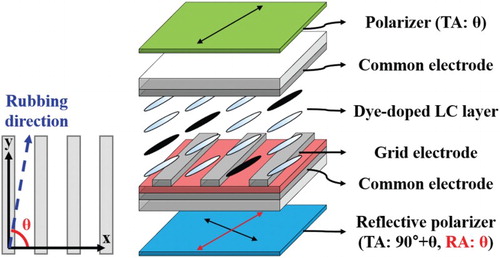
The structure of the proposed device is shown in Figure . The transmission axis (TA) of the top polarizer is perpendicular to the TA of the R-polarizer and parallel to the RA of the R-polarizer. A DDLC cell is placed between the top polarizer and the bottom R-polarizer, in which LC molecules are aligned parallel to the RA of the R-polarizer. The LC molecules are also aligned along angle θ. A three-terminal electrode, which includes the top common electrode, is used in this structure [Citation8–10]. The structure of the bottom substrate is the same as that of the conventional fringe-field-switching LC cell, which has grid electrodes and a bottom common electrode [Citation11]. A vertical electric field is applied between the top and bottom electrodes, and a fringe electric field is applied between the grid and bottom electrodes.
Figure 1. Structure of the proposed device.
The dichroic dye, which is doped to the host LC, absorbs the light polarized along the molecular axis and transmits the light polarized perpendicular to the molecular axis. The dye molecules that are doped to the host LC follow the movement of the LC directors. Based on the Beer–Lambert law, the normalized transmittance of a homogeneous DDLC cell is given by
(1)
(2)
where
and
are the transmittance and absorption coefficients for the directions parallel and perpendicular to the absorption axis of the dichroic dye material, respectively; c is the concentration of the dichroic dye; and d is the cell gap [Citation12]. Absorption coefficients
and
affect the dark and bright states, respectively. The contrast ratio can be expressed as follows:
(3)
As shown in Equation (3), the contrast ratio is determined by the difference between the absorption coefficients of the dichroic dye.
The operation of the proposed device in the transmissive and reflective modes is shown in Figure . To explain the operation of the proposed device, it is assumed that the angle θ is 90°. In the dark state of the transmissive mode, the light from the backlight unit passes through the R-polarizer and becomes linearly polarized along angle 0°. When it passes through the DDLC layer, the polarization state is not changed because the DDLCs are aligned parallel to the TA of the top polarizer. After passing through the DDLC layer, the polarization direction of the light is perpendicular to the TA of the top polarizer so that the dark state is obtained. The ambient light is also absorbed by the DDLC layer in the dark state.
Figure 2. Operating principles of the proposed device.
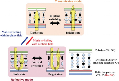
The bright state is achieved by applying an in-plane field between the grid electrodes and the bottom common electrode. The LC molecules are twisted along the field direction. As the light that is linearly polarized along angle 0° passes through the cell with polarization perpendicular to the molecular axis of the dichroic dye, little light absorption is expected.
When the device is operated in the reflective mode, the ambient light is linearly polarized along a 90° angle after passing through the top polarizer. The light is elliptically polarized after passing through the π-twisted DDLCs, and is partially reflected by the R-polarizer. At the same time, the linearly polarized light also passes through the cell with polarization perpendicular to the molecular axis of the dichroic dye, and the light is strongly absorbed simultaneously. After reflection by the R-polarizer, the polarization state is changed, and the light is absorbed by the polarizer. The reflected light is linearly polarized along a 90° angle, and the light is again strongly absorbed, whereby the dark state of the reflective mode can be obtained.
To achieve the bright state, the LCs are vertically aligned by applying a vertical field to the DDLC layer. Then, the polarization state does not change, and there is little absorption of the ambient light by the DDLC layer because the dye molecules are also aligned vertically. The light is reflected intact by the R-polarizer because the RA of the R-polarizer and the TA of the top polarizer are parallel to each other, so that the bright state is obtained.
In the transmissive mode, the dark state can be obtained by aligning the homogeneously aligned DDLC layer along the TA of the top polarizer. The dark state can be obtained in the reflective mode because the ambient light passes through the absorption axis of the DDLCs and is strongly absorbed by the dichroic dyes. As the reflectance of the dark state, however, depends on the mixing ratio of the dye, there is a need to dope a large amount of dichroic dye for a good dark state. Changing the polarization state also helps reduce the reflectance of the dark state. To be absorbed by the polarizer, the polarization direction has to be changed to from 90° to 0° when passing through the R-polarizer. A 90°-twisted LC layer can change the polarization direction from 90° to 0°, but it cannot maintain the 90°-twisted state when the applied electric field is removed. It returns to the homogeneously aligned deformation. Therefore, another stable LC deformation is needed for the dark state of the reflective mode.
For this concept, the BCSN mode can be a proper mode because it has two stable states: the splay state, in which the LCs are aligned in one direction; and the π-twist state, in which the LCs are twisted by 180° [Citation13,Citation14]. The π-twist state can be used for the dark state of the reflective mode because it can change the polarization state and maintain its deformation. This is the reason that the splay and π-twist states of the BCSN mode are employed for the transmissive and reflective modes, respectively.
As mentioned earlier, to reduce the reflectance of the dark state in the reflective mode, the LC deformation has to be different from that of the transmissive mode. The splay state of the BCSN mode is used as the initial state of the transmissive mode whereas the π-twist state of the BCSN mode is used as the initial state of the reflective mode. For mode switching between the transmissive and reflective modes, an appropriate electric field is applied for texture transition, as shown in Figure . When a switch is made to the transmissive mode from the reflective mode, a vertical field is required for transition from the splay state to the π-twist state. When a vertical field is applied for a short duration, the bend state is relaxed to the π-twist state. For switching to the reflective mode from the transmissive mode, an in-plane field is needed for transition from the π-twist state to the splay state. When an in-plane field is applied, the π-twist state returns to the initial splay state in the region affected by the applied in-plane field. After removing the in-plane field, entire region of the device is relaxed to the splay state.
When the ratio between the cell gap and the pitch length (d/p) is 0.25 in the BCSN mode, the 0°- and 180°-twist states have the same minimum free energy so that the splay and the π-twist state can be maintained permanently [Citation15]. When the d/p is 0.25, however, it is hard to make a transition from the π-twist state to the splay state over the entire region because the in-plane field exerts an influence only locally. Therefore, the π-twist and splay states coexist at the same time. To make a transition from the π-twist state to the splay state over the entire region, the d/p is set to 0.2. The π-twist state with the d/p set to 0.2, however, cannot be maintained permanently. To maintain the dark state in the reflective mode for a long time, a vertical electric field must be applied for 10 min [Citation16,Citation17].
3. Design of the proposed device
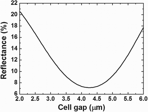
To find the optimum cell gap, the cell gap value that leads to the lowest reflectance at the π-twisted state in the proposed structure was calculated using the Jones matrix method [Citation18]. The parallel rubbing direction was set to 80°. The reflectance of the proposed structure when it is in the π-twist state, in which the LCs on each substrate are aligned along the RA of the R-polarizer, can be expressed without considering the light absorption by the dichroic dye, as follows:
(4)
where Δn, d, and λ are the optical anisotropy of the LC, the cell gap, and the wavelength of the incident light, respectively. The design was made at a 550 nm wavelength for the optical anisotropy of 0.1322. Through numerical calculation using Equation (2), the lowest reflectance of 7.1% was obtained for a cell gap of 4.3 µm, as shown in Figure . A perfect dark state could not be obtained because the π-twisted deformation of the LC layer could not perfectly change the polarization direction from 80° to −10°.
Figure 3. Calculated reflectance of the reflective mode in the π-twist state vs. the cell gap.
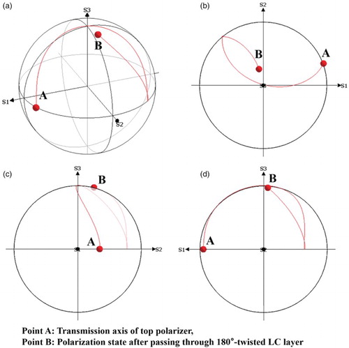
To confirm the change of the polarization state by the π-twisted deformation, numerical calculation was performed using the commercial software TechWiz LCD 1D (Sanayi System Co., Ltd., South Korea). Figure shows the polarization change on the Poincaré sphere without considering the light absorption by the dichroic dye. Under the calculated condition, when the ambient light passes through the top polarizer and the π-twisted LC layer, the 80°-polarized light at point A moves to the elliptical polarization state at point B around the -S3 axis. After passing through the LC layer once, the polarization state of the ambient light is changed to near the circular polarization state, and then about half of the light is reflected by the R-polarizer. After the round trip through the proposed structure, 92.9% of the ambient light is absorbed by the polarizer because of the change in the polarization state. Moreover, as the dye molecules also absorb the light, a good dark state can be obtained.
Figure 4. Change of polarization on the Poincaré sphere without considering the light absorption by the dichroic dye. (a) Poincaré sphere; (b) S1–S2 plane; (c) S2–S3 plane; and (d) S1–S3 plane.
To evaluate the electro-optic characteristics of the proposed device, a unit cell employing the structure shown in Figure was investigated both numerically and experimentally. The width of the bottom grid electrodes and the gap between them were chosen to be 2.8 and 4 m, respectively. A positive LC (ZLI-2293; Δε: 10; Δn: 0.1322) was mixed with black dichroic dye (S-428;
: 30.45;
: 2.78) and a chiral material (S811) to produce an LC mixture. The mixing ratios of the dye were 1.5 and 3 wt%, and the d/p of the chiral material was set to 0.2. A homogenous alignment layer (PIA-5310) was spin-coated onto the top and bottom substrates. The parallel rubbing direction was set to 80°. The fabricated device was maintained at a cell gap of 4.3 µm.
4. Results and discussion
4.1. Transmittance and reflectance vs. voltage
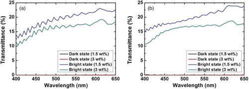
Figures and show the calculated and measured voltage-transmittance/reflectance curves of the proposed device, respectively. In the transmissive mode, the measured transmittances agreed well with the calculated values. When the mixing ratios of the dichroic dye were 1.5 and 3 wt%, the calculated transmittances of the bright state were 21 and 17.3% at 8.5 V, as shown in Figure (a). The calculated transmittances were 0% in both cases. The measured transmittances of the bright state were 19.9% and 16.1% at 6.2 V, as shown in Figure (b). The measured transmittances of the dark state were 0.02% in both cases. Figure (a) and (b) shows the calculated and measured transmission spectra of the proposed device in the transmissive mode. The transmittance spectra were obtained using the MCPD-3000 spectrometer (Photal). It was found that the measured transmittance spectra were similar to the calculated ones.
Figure 5. (a) Calculated and (b) measured transmittances vs. the applied voltage of the proposed device with the mixing ratio of the dichroic dye as a parameter.
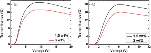
Figure 6. (a) Calculated and (b) measured reflectances vs. the applied voltage of the proposed device with the mixing ratio of the dichroic dye as a parameter.
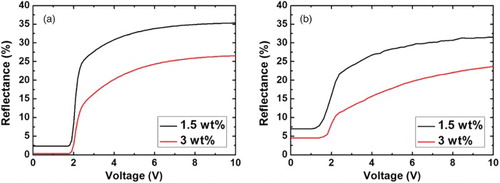
Figure 7. (a) Calculated and (b) measured transmittance spectra of the proposed device with the mixing ratio of the dichroic dye as a parameter.
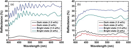
Contrary to the transmissive mode, the measured reflectances were quite different from the calculated results. When the mixing ratios were 1.5 and 3 wt%, the calculated reflectances of the dark state were 2.29% and 0.36%, respectively, and those of the bright state were 35.32% and 26.54% at 10 V. The measured reflectances of the dark state, however, were 7% and 4.5% when the mixing ratios were 1.5% and 3%, respectively. The measured results were different from the calculated ones due to the surface reflection by the glass substrate. The measured reflectances of the bright state were 31.4% and 23.7% at 10 V when the mixing ratios were 1.5% and 3%, respectively. Figure (a) and (b) shows the calculated and measured reflectance spectra of the proposed device in the reflective mode. It was found that measured reflectance spectra were similar to the calculated ones. As shown in Figures and , the maximum transmittance and reflectance decreased as the mixing ratio of the dichroic dye was increased.
Figure 8. (a) Calculated and (b) measured reflectance spectra of the proposed device with the mixing ratio of the dichroic dye as a parameter.
4.2. Reflectance of the dark state under the homogeneously aligned and π-twisted deformation
To confirm the improvement of the dark state in the reflective mode, the reflectance of the π-twisted deformation was compared with that of the homogeneously aligned deformation reported in [Citation7]. The DDLCs are aligned parallel to the RA of the R-polarizer in homogeneously aligned deformation whereas they are twisted by 180° and the LCs on each substrate are aligned parallel to the RA of the R-polarizer in π-twisted deformation. Figure (a) and (b) shows the calculated and measured reflectances, respectively. When the mixing ratios of the dichroic dye were 1.5 and 3 wt%, the calculated reflectances were 7.84% and 1.37% in the homogeneously aligned deformation and 2.29% and 0.36% in the π-twisted deformation. The measured reflectances were 12.94% and 5.2% in the homogeneously aligned deformation, and 7% and 4.5% in the π-twisted deformation.
Figure 9. Dependence of the (a) calculated and (b) measured reflectances of the dark state in the homogeneously aligned and π-twisted deformation on the mixing ratio of the dichroic dye.
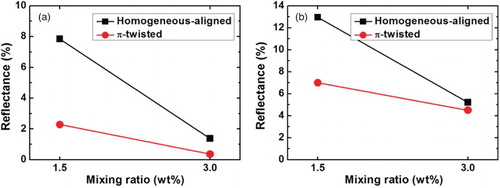
As expected, the π-twisted deformation has lower reflectance than the homogenously aligned deformation. When the DDLC layer is in the homogeneously aligned deformation, the dark state is obtained only by the light absorption of the dichroic dyes. As a homogeneously aligned DDLC layer could not lead to phase retardation, the light that passed through the TA of the top polarizer is reflected intact by the R-polarizer. On the contrary, the light is simultaneously absorbed by the dichroic dyes and the polarizer in the π-twisted deformation. After passing through the π-twisted deformation, the linearly polarized light is changed to elliptically polarized light and is partially reflected by the R-polarizer. For the round trip, the light absorption by the polarizer and the dichroic dye occurs twice, but despite the improvement of the dark state, further improvement of the dark state is still needed. As the linearly polarized light is changed to elliptically polarized light by the π-twisted deformation, there is a remaining component that can be reflected by the R-polarizer. Another reason for the poor dark state in the reflective mode is the surface reflection by the glass substrate. To overcome this problem, anti-reflection coating of the panel is needed.
5. Conclusion
Proposed herein is a single-panel DDLC device without subpixel division that is switchable between the transmissive and reflective modes. The BCSN mode, which has two stable states, was employed for the device. The splay and π-twist states of the BCSN mode were used as the dark states of the transmissive and reflective modes, respectively. As a result, a good dark state was obtained in both the transmissve and reflective modes. It is believed that the proposed device can be applied in various display devices that can be used under outdoor as well as indoor environments.
Additional information
Notes on contributors

Ahn-Ki Kim
Ahn-Ki Kim received his B.S. in Electronics Engineering degree in 2014 from Pusan National University in Busan, South Korea, where he is currently working towards an M.S. degree in the same field. His major research interest is LCD design.

Tae-Hoon Yoon
Tae-Hoon Yoon received his B.S. in Electronics Engineering degree from Seoul National University in 1979, and his M.S. and Ph.D. in Electrical Engineering degrees from Korea Advanced Institute of Science and Technology (KAIST) in 1982 and 1986, respectively. Since 1986, he has been with the Department of Electronics Engineering of Pusan National University in Busan, South Korea, where he is currently a professor. In 1990, he worked as a research scientist at the Optical Sciences Center of the University of Arizona, and in 1997, he worked as a visiting scholar at the Department of Electrical and Computer Engineering of the University of California in Santa Barbara, USA. From 2001 to 2003, he served as the full-time program director for the Information & Electronics Program of the Korea Institute of S & T Evaluation and Planning. He has authored/co-authored 199 international journal papers to date, and currently has 78 issued and pending patents. His current research interests include optical design of LCDs, LC light shutter, and fast switching of LCs.
Dr Yoon chaired the Program Committee of IMID (International Meeting on Information Display)/IDMC (International Display Manufacturing Conference)/Asia Display 2010. He also chaired the Executive Committee of IMID (International Meeting on Information Display) 2011. In 2012, he served as the President of the Optical Society of Korea. He has been the editor-in-chief of the Journal of Information Display since 2014. He is also the Organizing Committee chair of ACLC (Asian Conference on Liquid Crystals) 2015. He was awarded Best Researcher of Pusan National University in 2012.
References
- G.-S. Lee, J.-C. Kim, and T.-H. Yoon, Jpn. J. Appl. Phys. 46 (1), 289 (2007). doi: 10.1143/JJAP.46.289
- J.-H. Lee, X. Zhu, Y.-H. Lin, W.-K. Choi, T.-C. Lin, S.-C. Hsu, H.-Y. Lin, and S.-T. Wu, Opt. Express. 13 (23), 9431 (2005). doi: 10.1364/OPEX.13.009431
- K.-H. Kim, H.-J. Jin, B.-H. Cheong, H.-Y. Choi, S.-T. Shin, J.-C. Kim, and T.-H. Yoon, Appl. Opt. 49 (25), 4774 (2010). doi: 10.1364/AO.49.004774
- H.-J. Jin, K.-H. Kim, H. Jin, J.-C. Kim, and T.-H. Yoon, J. Inf. Disp. 12 (1), 17 (2011). doi: 10.1080/15980316.2011.555510
- T. Maeda, T. Matsushima, E. Okamoto, H. Wada, O. Okumura, and S. Iino, J. Soc. Inf. Disp. 7 (1), 9 (1999). doi: 10.1889/1.1985264
- Y. Li, X. Wu, and S.-T. Wu, J. Disp. Technol. 5 (8), 335 (2009). doi: 10.1109/JDT.2009.2027033
- K.-H. Kim, D.-H. Song, H.-J. Jin, and T.-H. Yoon, J. Phys. D: Appl. Phys. 44 (29), 295101 (2011). doi: 10.1088/0022-3727/44/29/295101
- J.-I. Beak, K.-H. Kim, J.-C. Kim, T.-H. Yoon, H.-S. Woo, S.-T. Shin, and J.-H. Souk, Jpn. J. Appl. Phys. 48, 104505 (2009). doi: 10.1143/JJAP.48.104505
- T.-H. Choi, J.-W. Kim, and T.-H. Yoon, J. Disp. Technol. 10 (12), 1088 (2014). doi: 10.1109/JDT.2014.2346175
- T.-H. Choi, Y.-J. Park, J.-W. Kim, and T.-H. Yoon, Liq. Cryst. 42 (4), 492 (2015). doi: 10.1080/02678292.2014.1000987
- S.-H. Lee, S.-L. Kim, and H.-Y. Kim, Appl. Phys. Lett. 73 (20), 2881 (1998). doi: 10.1063/1.122617
- S.-T. Wu and D.-K. Yang, Reflective Liquid Crystal Displays (Wiley, Hoboken, NJ, 2001).
- S.-H. Lee, K.-H. Park, T.-H. Yoon, and J.-C. Kim, Appl. Phys. Lett. 82 (24), 4215 (2003). doi: 10.1063/1.1581368
- T.-H. Kim, J.-H. Lee, T.-H. Yoon, and S.-W. Choi, Opt. Express. 20 (14), 15522 (2012). doi: 10.1364/OE.20.015522
- C.-G. Jhun, C.-P. Chen, S.-L. Lee, J.-I. Baek, T.-H. Yoon, and J.-C. Kim, Jpn. J. Appl. Phys. 45 (6A), 5063 (2006). doi: 10.1143/JJAP.45.5063
- C.-G. Jhun, C.-P. Chen, U.-J. Lee, S.-R. Lee, T.-H. Yoon, and J.-C. Kim, Appl. Phys. Lett. 89 (12), 123507 (2006). doi: 10.1063/1.2354430
- S.-R. Lee, J.-H. Lee, C.-G. Jhun, S.-B. Kwon, T.-H. Yoon, and J.-C. Kim, J. Appl. Phys. 108 (07), 074508 (2009). doi: 10.1063/1.3103769
- P. Yeh, Optics of Liquid Crystal Displays (Wiley, New York, 1999).