
ABSTRACT
A pixel circuit that compensates for the non-uniform thin-film transistor (TFT) characteristics across a display panel is inevitably used in the organic light-emitting diode (OLED) display to exhibit uniform brightness. The existing pixel circuits aim to compensate only for the non-uniformity of the threshold voltage (Vth). They do not compensate for the deviation of the other parameters, such as the mobility and the subthreshold swing. In this study, how the OLED current changes when the mobility of a TFT in the Vth compensation circuit increases was examined. If the mobility increases, the enhanced drain current drives the TFT into a deeper subthreshold mode during the Vth compensation phase, and the |VGS| of the TFT decreases compared with the normal mobility case. The resultant OLED current, however, can be higher or lower than the normal mobility case depending on the gray level because the effects of the current increase due to the higher mobility and of the current decrease due to the reduced |VGS| appear simultaneously but differently depending on the VGS value of the TFT. The analysis results show that the OLED current increases for the high gray level but decreases for the low gray level. It remains almost unaffected by the mobility increase for the mid-gray level.
1. Introduction
The organic light-emitting diode (OLED) displays recently replaced the liquid crystal displays (LCDs) for mobile devices such as smartphones, owing to the high flexibility, better image quality, and lower power consumption of OLED. It is troublesome, however, to exhibit uniform brightness on the OLED display panel compared with the LCD because the brightness of the OLED pixel is determined by the current in each pixel rather than by the voltage stored in a capacitor, which is the method used in the LCD. The pixel of the OLED display also stores the data voltage supplied by a driver IC, which is very uniform. In the case of the OLED display; however, an additional conversion process from the data voltage to the pixel current is required. This voltage-to-current conversion is carried out by a thin-film transistor (TFT) in each pixel. In the process of conversion, severe mura appears when the characteristics of the TFT are not sufficiently uniform. Therefore, a pixel circuit is needed to compensate for the TFT non-uniformity and to have a uniform voltage-to-brightness relation.
For example, in the case of the low-temperature polycrystalline silicon (LTPS) TFT, the device parameters such as the carrier mobility, threshold voltage (Vth), and subthreshold swing vary depending on the random distribution of the grain boundaries in the polycrystalline silicon (poly-Si) film [Citation1,Citation2]. The conventional pixel circuits are designed to compensate only for the variation of the Vth of the TFT [Citation3–8]. The Vth compensation is more effective than the compensation of other parameters, such as the mobility and subthreshold swing, because the OLED-driving TFT operates around the threshold point to realize a high contrast ratio, and the variation of Vth critically affects the TFT current in this bias range. The mobility variation, however, may also influence the uniformity of the TFT current, but the effects of the mobility variation on the TFT current in the Vth compensation circuit have not yet been investigated. Reported in this paper is how the compensated-for OLED current varies when the mobility of the TFT increases in the conventional Vth compensation circuit.
2. Operation of the Vth compensation pixel circuit
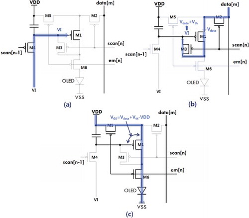
shows Choi’s 6T1C Vth compensation circuit, which was used in the analysis [Citation1]. This circuit has been used in the Samsung smartphones for nearly 10 years. The operation of the pixel circuit consists of three phases, as shown in the timing diagram in (b). First, in the initializing phase, the OLED-driving TFT M1 is turned on by the initialization voltage (VI), which is supplied through M4, as shown in (a). Therefore, the previous data stored in the capacitor are deleted. Then, in the programing phase, a new data voltage is supplied to the source terminal of M1 through M2, as shown in (b). During this phase, current flows through M1 because the gate potential of M1 is VI, which is sufficiently lower than the data voltage that is the source potential of M1. The current that flows through M1 raises the potential of the gate node of M1. At the end of the programing phase, the VGS of M1 approaches the Vth of M1, and the current decreases sharply. Accordingly, the gate potential of M1 becomes Vdata + Vth. Finally, it turns into the emission phase, and the VGS of M1 becomes Vdata + Vth − VDD, which is stored in the storage capacitor, as shown in (c). As a result, the OLED current that is identical to the current of M1 is determined independently of the Vth of M1, as expressed by Equation (1). Other Vth compensation circuits work in a similar way [Citation3–8].
(1)
Figure 1. (a) PMOS 6T1C Vth compensation pixel circuit in Ref. [Citation1]; (b) its timing diagram.
![Figure 1. (a) PMOS 6T1C Vth compensation pixel circuit in Ref. [Citation1]; (b) its timing diagram.](/cms/asset/6d9af6f3-69a1-4680-adde-9a5fa5030186/tjid_a_1259128_f0001_c.jpg)
Figure 2. (a) Initializing phase, (b) programing phase, and (c) emission phase of the 6T1C circuit operation process.
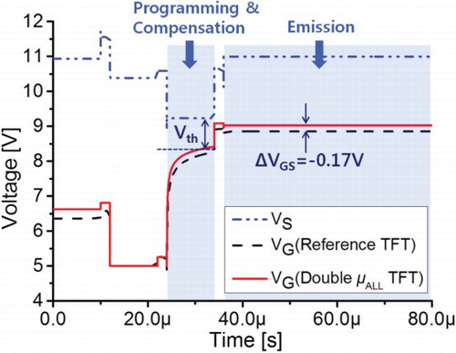
shows the waveforms of gate voltage VG and source voltage VS of M1 during the operation shown in . It should be noted that VG (red solid and black dashed lines) approaches VS (blue dash-dot-dot line) with a voltage gap corresponding to the Vth of M1 during the programing and compensation phase. At the end of this phase, the speed of VG change slows down because the current of M1 decreases as it enters the subthreshold mode. In , it can also be verified that the rate of VG change depends on the carrier mobility of M1. VG changes faster when the mobility is higher (red solid line). From this result, it can be expected that mobility deviation may affect the compensated-for VGS value.
Figure 3. Waveforms of the gate and source voltages of M1 TFT during the operation phases for the different mobility cases.
3. Mobility parameters in the spice model
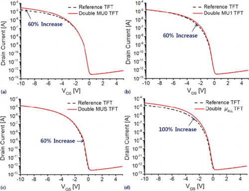
To investigate the effects of TFT mobility on the Vth compensation circuit, a SmartSpice simulator and the Rensselaer Polytechnic Institute (RPI) poly-Si TFT model (level 36) were used. shows the device parameters constituting the TFT model. These parameters determine the current-to-voltage characteristics of the device synthetically according to the bias condition. In this analysis, only three parameters were controlled: MU0, MU1, and MUS, which are directly related to the mobility of the TFT. MU0 means high-field mobility and influences the current of TFT when VGS is high. MU1 means low-field mobility and influences the current of TFT when VGS is close to Vth. MUS means subthreshold mobility and influences the current of TFT in the subthreshold mode.
Table 1. RPI poly-Si TFT model parameters for spice simulation.
How these three parameters affect the transfer characteristics of the TFT model was examined. shows the transfer characteristics when MU0, MU1, and MUS are doubled, respectively. The simulation condition was VDS = −10 V, and the channel width and length of the TFT were 2 and 10 μm, respectively. Each parameter increased a different part of the transfer characteristics. When only MU0 was doubled, the TFT current noticeably increased for VGS < −3 V, and by as much as 60% for VGS < −9 V, as shown in (a). As can be seen in (b), when only MU1 was doubled, the TFT current increased for the VGS close to the Vth, and the maximum increase was 60% for the VGS slightly above the Vth. As shown in (c), when only MUS was doubled, only the subthreshold current increased, and by about 60%. When all the three parameters were doubled at the same time, the overall TFT current increased by more than 80%, except for the leakage current, as shown in (d). The maximum increase of the TFT current was about 100% for the VGS slightly above the Vth. In the following analysis, only the case in which all the three mobility parameters were doubled were considered because the overall current could increase if the poly-Si film quality of the fabricated TFT was better than the reference.
Figure 4. Transfer characteristics of the TFT models for (a) high-field mobility (MU0) doubling, (b) low-field mobility (MU1) doubling, (c) subthreshold mobility (MUS) doubling, and (d) all the mobilities’ (MU0, MU1, and MUS) doubling when VDS = −10 V and TFT’s W/L = 2 μm/10 μm.
4. Results
As shown in , during the programing and compensation phase, the VG of the double-mobility TFT rose faster than the VG of the reference TFT because the current of the double-mobility TFT was higher. At the end of this phase, the difference between the two VG’s was about 0.17 V. This difference, in principle, was almost independent of the data voltage (i.e. the gray level) because the VGS of M1 approached Vth irrespective of the data voltage. In the next phase, the VS of M1 for both cases became VDD, and the difference of the VGS between the different mobility cases remained as 0.17 V. In other words, the absolute value of VGS, |VGS|, was smaller during the emission phase, when the mobility was higher.
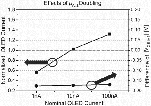
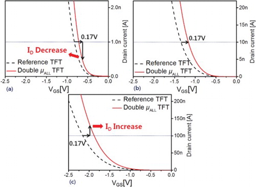
shows how the OLED current changed when the mobility was doubled compared with the reference case. As mentioned earlier, the difference of |VGS.M1| between the two cases had an almost constant value (0.17 V) in all the OLED current cases (1, 10, and 100 nA). The OLED current of the double-mobility case, however, could be larger or smaller compared with the reference case because the mobility as well as the VGS determined the current simultaneously according to Equation (1). When the OLED current of the reference case was 10 nA, there was little difference, although the mobility was doubled. The effect of the mobility increase was canceled out by the |VGS.M1| decrease. In the case of 1 nA, however, although the difference of |VGS.M1| was the same (0.17 V), the current of the double-mobility case decreased by more than 40% compared with the reference case because the current-increasing effect due to the mobility increase was smaller than the effect of the |VGS.M1| decrease. In contrast, in the case of 100 nA, the difference of |VGS.M1| was also 0.17 V, but the current increased by about 32% because the current-increasing effect due to the mobility increase was larger than the effect of the |VGS.M1| decrease.
Figure 5. Effects of all the mobilities’ doubling on the programed |VGS.M1| values, and resultant OLED currents vs. the various target currents.
shows the transfer characteristics of M1 for the cases when the OLED current was 1, 10, and 100 nA. For the low gray level (1 nA, (a)), the TFT was in the subthreshold mode, and the effect of the |VGS.M1| decrease was stronger (exponentially proportional) than the effect of the mobility increase. Therefore, the current decreased for the 1 nA case. For the mid-gray level (10 nA, (b)), the TFT was slightly above the threshold condition, and the effect of the mobility increase was almost compensated for by the |VGS.M1| decrease during the Vth compensation phase. For the high gray level (100 nA, (c)), the bias condition of the TFT was sufficiently above the threshold voltage, and the effect of the mobility increase was stronger than that of the |VGS.M1| decrease because the current was proportional merely to the square of VGS (not in the exponential proportion). Accordingly, the current increased for the 100 nA case.
Figure 6. Different effects of the programed |VGS.M1| decrease on the OLED currents for various target currents: (a) 1 nA; (b) 10 nA; and (c) 100 nA.
5. Conclusion
The pixel current of the OLED display employing a Vth compensation circuit can be affected by the mobility variation of the TFTs. The compensated-for OLED current tends to decrease for the low gray level but to increase for the high gray level when the mobility increases because the effect of the current increase due to the higher mobility and that of the current decrease due to the reduced |VGS| during the emission phase appear simultaneously but differently depending on the VGS value of the TFT. When the TFT is in the deep subthreshold mode, the effect of a reduced |VGS| is stronger than that of mobility increase. The effect of mobility increase is stronger, however, than that of |VGS| decrease when the TFT is sufficiently above the threshold point.
Reported in this paper is only the effect of double-mobility increase on the operation of the Vth compensation pixel circuit. The same trend of current variation was also verified, however, when the mobility increase is less than twofold, although it is not presented in this paper.
Disclosure statement
No potential conflict of interest was reported by the author.
Additional information
Notes on contributors

YoungHa Sohn
YoungHa Sohn received his B.S. Electronics Engineering degree from Konkuk University in 2015 and is now an M.S. candidate in the same university. His main interests are characterization of LTPS TFTs, the pixel compensation circuit of the OLED display, and the driving circuit of the display panel.

GeumJu Moon
GeumJu Moon received his B.S. Electronics Engineering degree from Konkuk University in 2015 and is now an M.S. candidate in the same university. His main interests are analyses of the TFT characteristics and of power devices such as IGBT.

KwangHyun Choi
KwangHyun Choi received his B.S. Nano-Science and Mechanical Engineering degree from Konkuk University Glocal Campus in 2016 and is now an M.S. candidate in Konkuk University, Seoul. He has been researching on the analysis of the driving circuit for displays, and on designing the layout of a pixel circuit for mobile displays.

YongSang Kim
YongSang Kim received his B.S., M.S. and Ph.D. Electrical Engineering degrees from Seoul National University, Seoul, South Korea in 1988, 1990, and 1994, respectively. He was a professor at Myongji University from 1995 to 2013, and at Sungkyunkwan University from 2013. His research interests are the organic-transistor-based biosensor, organic solar cells, oxide TFTs, and solution-processing technologies for organic electronic devices.

KeeChan Park
KeeChan Park received his B.S., M.S. and Ph.D. Electrical Engineering degrees in 1997, 1999, and 2003, respectively, from Seoul National University, Seoul, South Korea. He worked as a senior engineer at Samsung Electronics from 2003 to 2007. From 2007 to the present, he has been a professor at Konkuk University. His research areas include the design of display panels, circuit integration using TFTs, and device characterization.
References
- S.H. Jang, B.T. Son, S.H. Choi, D.J. Kim, G.S. Kim and M.H. Yoo, SID Symp. Dig. Tech. Pap. 47, 1162 (2016). doi: 10.1002/sdtp.10856
- C.W. Yang and P. Su, IEEE Trans. Electron Dev. 61, 1211 (2014). doi: 10.1109/TED.2014.2308951
- S.M. Choi, O.K. Kwon, N. Komiya and H.K. Chung, IDW 4, 535 (2003).
- Y.W. Kim, W.K. Kwak, J.Y. Lee, W.S. Choi, K.Y. Lee, S.C. Kim and E.J. Yoo, SID Symp. Dig. Tech. Pap. 40, 85 (2009). doi: 10.1889/1.3256930
- J.H. Lee, J.H. Kim and M.K. Han, IEEE Electron Dev. Lett. 26, 897 (2005). doi: 10.1109/LED.2005.859625
- C.L. Lin and Y.C. Chen, IEEE Electron Dev. Lett. 28, 129 (2007). doi: 10.1109/LED.2006.889523
- H.Y. Lu, T.C. Chang, Y.H. Tai, P.T. Liu and S. Chi, J. Display Technol. 3, 398 (2007). doi: 10.1109/JDT.2006.890696
- D.W. Park, C.K. Kang, Y.S. Park, B.Y. Chung, K.H. Chung, K.N. Kim, B.H. Kim and S.S. Kim, J. SID 19, 329 (2011).