
ABSTRACT
Curvature is an important concept for understanding layering structures in soft matters, ranging from complex macromolecular self-assembled structures to simple lipid bilayers. Among the various kinds of soft matters, smectic liquid crystal (LC) phases have been widely studied because of their periodic featured curvatures under various external forces. Generally, their curvatures are on the micron-scale due to the bulk elasticity of smectic LC materials. In this review, a combination of sublimation and recondensation of smectic LC materials generates a variety of curvatures at the nanometer scale, which cannot be achieved by self-assembly under thermal equilibrium conditions. In particular, we have focused on the change of curvatures in focal conic domains under non-equilibrium conditions, in which negative and zero Gaussian curvatures in the micron-scale transform to positive Gaussian curvatures in the micron- and nanometer scales. Finally, the review closes with applications using such non-equilibrium self-assembly of smectics.
1. Introduction
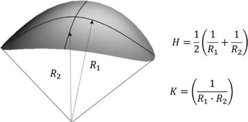
Curvatures of soft matters are of interest for both fundamental scientific research and a number of potential applications. Common examples of curvatures are found in cell membranes, organelles, proteins, block copolymers, and liquid crystals (LCs) [Citation1–7]. Curvatures of soft matters are varied depending on intermolecular interactions and stimuli-responsive characteristics [Citation8–13]. Generally, a curvature can be described by its mean curvature H and Gaussian curvature K, which are given by two principal radii of curvature, R1 and R2, as shown in . Thus, curved surfaces of differential geometries in soft matters allow us to define the topological features and symmetry, and understand structural functions for practical applications. For example, the biconcave disc-like shape of a red blood cell, consisting of a phospholipid bilayer and the underlying two-dimensional network of spectrin molecules, plays a crucial role for the fast gas exchange between hemoglobin and the surrounding medium, enabling flexible migration into various vessels including capillary vessels of smaller size than the red blood cells [Citation14]. Block copolymers are another example, being a material frequently used in the fabrication and engineering of nanostructures. These can show a variety of curvatures such as spheres, cylinders, and lamella are gyroids depending on the volume fraction of each block, which can be used in patterning applications [Citation15–22].
Figure 1. Local geometry and interfacial curvature described by mean and Gaussian curvatures (H, K).
The curvatures of soft matters have been extensively studied in biology, polymer science, and other related fields. However, the understanding and control of soft matter curvatures is still limited because of the poor orientation control of bulk curvatures and extremely complicated morphogenesis mechanisms. Thus, many platforms have been suggested to simplify and control complex curvatures, the most representative involving the use of low molecular weight LC materials that can easily and quickly form various curvatures [Citation22–26]. Among these LC phases, smectic phases having layers between bulk molecules can show dramatic changes in morphogenesis compared to a nematic phase that has only orientation order, showing a variety of curvatures in various boundary conditions [Citation27,Citation28]. Furthermore, complex architectures in biological systems are similar to the layering structures of smectics that can have specific topologies and textures; thus, this platform can provide a more intimate understanding of morphogenesis in biomaterials [Citation29–35].
In general, smectic LCs show viscous but fluid behavior that enables layers to bend depending on the container shape, showing a very broad range of interesting morphologies as well as defects [Citation36–54]. One of the most well-known examples of these LCs is in focal conic domain arrays (FCDs) that have conjugated ellipse and hyperbola defect lines made of smectic layers. In particular, FCDs can show cusp-like structures when smectic LC materials are placed on a planar aligned solid substrate as a droplet exposed to air (or free surface conditions), which are known as toric FCDs (TFCDs) [Citation17,Citation44–53]. Unlike previously reported self-assembling materials that were geared toward defect-free structures of ordered molecules and components, in recent years, TFCD defects have been recognized as a promising candidate for building blocks in realizing many lithographic applications such as templates of colloidal assembly, micro lens arrays, soft lithography, functional surfaces, and photo masks [Citation50,Citation54–61]. Furthermore, researchers have attempted to develop new types of hierarchical arrangements of LC molecules in two or three dimensions by using modulated substrates that act as topographical templates [Citation48–52]. However, the featured curvature in TFCD shows a cusp-like shape in the equilibrium state, limiting the applications of TFCDs to micro-fabrication systems [Citation54]. In order to progress the application space even further using smectic layers in optoelectronics, biology, membranes, and novel nano-patterning, fundamental studies into the topology of soft matter, size reduction, and new types of curvatures in smectic LC phases are necessary, as pattering applications using block copolymers have been well developed in the sub-100 nm range [Citation62–66].
Recently, thermal treatment of smectic materials at the smectic LC phase temperature was shown to change the mean and Gaussian curvatures of smectic structures, in which negative to positive Gaussian curvature transformation was achieved via gradual peeling off and recondensation of smectic layers [Citation67]. Based on this phenomenon, three dimensional bent layered structures have emerged at the nanoscale, having quite different morphologies compared with original LC textures [Citation67,Citation68]. This kind of self-assembling behavior of soft matter systems under thermally non-equilibrium conditions could open a route to create such small feature structures as well as more exotic curvatures.
In this review, the smectic curvatures formed under thermal equilibrium will be discussed in Section 2, in which the basic smectic curvatures will be introduced. The sublimation property of semi-fluorinated materials, which is a key to achieve the nano-curvatures, and the morphogenesis of various curvatures of the smectics through sublimation and recondensation process will be discussed in Section 3. Last, we will introduce applications using these nano-curvatures, including fabrication of superhydrophobic surfaces, nanoparticle cluster arrays for illumination, and surface-enhanced Raman spectroscopy (SERS).
2. Curvatures in smectic LCs
The smectic phase is one of the primary LC phases, where the term, ‘Smectic,’ comes from the Latin ‘smecticus,’ meaning a sort of soap bubble. Among the various kinds of smectics, the smectic A phase has layers where LC molecules (rod-like or otherwise) are arranged in an almost perpendicular manner between layer planes ((a)), which emerges by cooling from an isotropic melt. Other smectic phases exist that have different molecular arrangement within the layers, which vary by the molecular structures and intermolecular interactions including π–π interactions, dipole–dipole interactions, and van der Waals forces [Citation69]. For example in the smectic C phase, molecules are tilt-arranged in the layer planes, which makes the layer structures in this phase more dense than those in the smectic A phase ((b)) [Citation70]. A biaxial smectic A phase is also possible, in which the layer normal vector described by the molecular director n, as found in the smectic phase, at the same time the smectic layers exhibit in an in-plane orientation order with the spontaneous breaking of rotational symmetry, which is known as the McMillan phase SmCM as suggested by de Gennes [Citation71]. Among the biaxial smectic phases, “B” phases are comprised bent core molecules [Citation72–74], with a chiral layering smectic phase B4 known as helical nanofilament being the most complex but interesting phase because the bent core molecules in the B4 phase do not have chiral centers unlike other chiral chemical compound systems ((c,d)) [Citation75–77]. This results from the saddle-splay deformation generated by the different molecular packing behaviors of aromatic core groups and alkyl tails, which are orthogonally tilted from the layer normal ((c)) [Citation75]. This sub-layer level of molecular packing enables the formation of helical smectic phases at the nanometer scale, with width (w) in the range of 20 < w < 54 nm and half pitch (hp) in the range of 100 < hp < 125 nm ((d)) [Citation77].
Figure 2. Schematic representation of molecular orientations of (a) smectic A phase and (b) smectic C phase. (c) Molecular structure of bent core LC known as NOBOW. The molecule has an inherent polar direction p and the tilt of the molecular plane, n, from the layer normal, s. (d) The scheme and transmission electron micrograph of the helical nano filament, having 5–8 twisted smectic layers of layer distance, d ∼ 4.5 nm, width of filament, w ∼ 35 nm and the half pitch, hp ∼ 110 nm. The layer edge (LE) region and layer surface (LS) region were observed by Kim et al. [Citation77].
![Figure 2. Schematic representation of molecular orientations of (a) smectic A phase and (b) smectic C phase. (c) Molecular structure of bent core LC known as NOBOW. The molecule has an inherent polar direction p and the tilt of the molecular plane, n, from the layer normal, s. (d) The scheme and transmission electron micrograph of the helical nano filament, having 5–8 twisted smectic layers of layer distance, d ∼ 4.5 nm, width of filament, w ∼ 35 nm and the half pitch, hp ∼ 110 nm. The layer edge (LE) region and layer surface (LS) region were observed by Kim et al. [Citation77].](/cms/asset/fc91dab4-a69d-4cde-a157-5e0f722c9b1a/tjid_a_1410500_f0002_c.jpg)
2.1. Periodic curvatures in SmA film: FCDs
Among the defect structures in smectics, the most common is FCDs, modeled as families of the so-called Dupin cyclides that appear like asymmetric donut shapes. Borrowing the expression of Lavrentovich and Kleman, in order to understand the morphogenesis of layers in FCDs, it is necessary to consider a simple saddle-like smectic layer and parallel additions of the same featured layers, Si, where their normals surround two focal surface F1 and F2, having centers of principal curvature C1 and C2 and normals indicating the molecular director, n ((a)) [Citation27]. These focal surfaces show singularities of the director field, where the order parameter of the smectic layers is broken, and the energy associated with the singularities scales with the area of the focal surfaces. Because the elastic energy is concentrated around the focal surfaces, the smectic layers want to have smaller areas. Therefore, focal surfaces are degenerated into two lines which are a paired hyperbola and ellipse (the ellipse is perpendicular to the plane including hyperbola), or even smaller, a point ((b)) [Citation71]. The shrinkage of the focal surfaces into a point results in a concentric packing of layers with spherical shapes, which is rarely found during the formation of FCDs with free surfaces but appears in the sublimable smectics that will be discussed in Section 3 [Citation68].
Figure 3. (a) Schematic illustration of a set of parallel layers Si, their normal n, the loci of centers of curvature C1 and C2, the focal surfaces F1 and F2. (b) The focal surfaces reduced into two conjugated line of ellipse and hyperbola by forming cyclides. The straight lines are layer normal vectors in the cyclides. Schematic sketches of (c) FCD-type 1, (d) FCD-type 2, and (e) FCD-type 3 [Citation27].
![Figure 3. (a) Schematic illustration of a set of parallel layers Si, their normal n, the loci of centers of curvature C1 and C2, the focal surfaces F1 and F2. (b) The focal surfaces reduced into two conjugated line of ellipse and hyperbola by forming cyclides. The straight lines are layer normal vectors in the cyclides. Schematic sketches of (c) FCD-type 1, (d) FCD-type 2, and (e) FCD-type 3 [Citation27].](/cms/asset/19b2c907-e22c-4d42-bcfe-73ff09b0e901/tjid_a_1410500_f0003_c.jpg)
There are three representative FCDs depending on the Gaussian curvatures of smectic layers [Citation27]. FCDs with negative Gaussian curvature that has R1·R2 < 0 are most commonly found in thermotropic smectic phases, classified as FCD-1 ((c)). The elastic free energy density of such FCDs can be described using the following equation [Citation71]:
(1)
is the saddle-splay elastic constant,
is a compression modulus and γ = (d − do) is a relative layer thickness change from its equilibrium value, do. The elastic free energy in FCDs prohibits bending and twisting the molecular director n. According to Equation (1), the minimum splay energy state is achieved with a negative Gaussian curvature. In contrast, FCD-2 has a positive Gaussian curvature and an onion-like shape ((d)). Although Sierro et al. reported FCD-2 in lyotropic smectic phase in 1997, FCD-2 has not yet been observed in thermotropic smectics [Citation78,Citation79]. FCD-3 takes the form of cyclides with both positive and negative Gaussian curvature layers, as introduced by Klemen and Lavrentovich ((e)) [Citation28].
Bidaux et al. have reported a special form of FCD-1, the TFCD, where the ellipse line is reduced into a circle and the hyperbola straightens and passes through the center of the circle [Citation80]. According to this work, TFCDs are generated when a smectic A LC material is placed in a hybrid aligned cell, where the Dupin cyclides are evolved to tori. In these conditions, the LC molecules prefer to align parallel to the bottom substrate, while they are perpendicularly aligned to the top substrate or LC/air interface. These conflicting anchoring conditions can be resolved by curving the smectic layers from the free surface to the bottom with a radius of curvature R1 ((a)). The curved layer is additionally folded in the horizontal plane to avoid wall defects with a radius of curvature R2 circling along with the axis of rotational symmetry. As a result of these curvatures, the folded layers are accommodated by two defect lines: a straight line perpendicular to the substrate and circular line at the base of TFCDs; the translational order of layering with equidistant thickness is broken at the two defect lines. For the curvatures in each TFCD, the layers adopt saddle-like shapes with a Gaussian curvature K = 1/(R1·R2) < 0. Each TFCD is smoothly connected to the flat layers of the peripheral part of TFCD (K = 0) as the cylindrical lateral borders of the TFCD meet each other in a hexagonal arrangement. (b) shows scanning electron microscopy (SEM) images presenting that the LC/free surface interface has a non-flat profile with cusp-like depressions at the straight line defect in the core of each TFCD. Characteristic Maltese cross-patterns are observed for each TFCD using optical microscopy, demonstrating that the projection of molecular orientation on the bottom substrate is radial with the borderline of the basis of the TFCDs (inset of (b)). Within the border area between the circular bases, the molecules are homeotropically aligned to the substrate. The hexagonally close-packed Maltese cross-patterns correspond to the hexagonal lattice of the cusps of TFCDs, in which the packing of TFCDs is unwilling to allow the existence of gaps between TFCDs, similar to the well-known Apollonius packing of circles [Citation81,Citation82].
Figure 4. (a) Diagram of a single TFCD cross-section. R1 and R2 are the principal radii of layer curvatures. The LC molecules are aligned along the layer normal line such as that connect the point of straight line defect with the point of circular line. Every layer adopts the negative Gaussian curvature, K = R1·R2 < 0. a is the radius of the TFCD. (b) Top-view SEM image of the TFCD film in equilibrium with hexagonal arrangement. The inset depicts the POM image corresponding to the TFCD, showing the projection of radial orientation of LC molecules at the basis of TFCD. (c–e) POM and SEM images (left column and right column, respectively) of TFCDs in microchannels of different depths h = 2, 5, 10 µm, and fixed width ∼50 µm [Citation47].
![Figure 4. (a) Diagram of a single TFCD cross-section. R1 and R2 are the principal radii of layer curvatures. The LC molecules are aligned along the layer normal line such as that connect the point of straight line defect with the point of circular line. Every layer adopts the negative Gaussian curvature, K = R1·R2 < 0. a is the radius of the TFCD. (b) Top-view SEM image of the TFCD film in equilibrium with hexagonal arrangement. The inset depicts the POM image corresponding to the TFCD, showing the projection of radial orientation of LC molecules at the basis of TFCD. (c–e) POM and SEM images (left column and right column, respectively) of TFCDs in microchannels of different depths h = 2, 5, 10 µm, and fixed width ∼50 µm [Citation47].](/cms/asset/7f4cea40-f5fd-4523-839f-3f008967c60e/tjid_a_1410500_f0004_c.jpg)
2.2. Energy of TFCDs: general remarks
Tangential orientation of smectic layers and molecules in TFCDs is resolved by the formation of TFCDs with radial configuration at the bottom substrate, where the molecules are preferentially oriented parallel to the substrate as mentioned previously. The free energy of TFCD formation is closely related to surface energy (Fs) and elastic energy (Fe), expressed as the difference ΔF = Fe + Fs. The surface energy, Fs, of TFCD is reduced by , in which a is the radius of TFCD,
and
are the surface energy densities for molecular orientation parallel and perpendicular to the bottom substrate, respectively, and
and
correspond to the surface energy density of the smectic LC/air interface associated with the depression of the free surface. However, the tangential configuration carries the elastic energy of the curved layers and defect cores, in which the free energy can be approximated as aαK (K is the curvature elastic constant of the smectic A phase, and α is a numerical factor between 1 and 10) [Citation28]. As a result of the equalization between two terms, the minimum size of a TFCD can be determined by
, which is on the order of 1–10 µm for typical estimates of K (∼10−11 N) and σsubs (∼10−5 J m−2) [Citation36,Citation37]. Thus, for a typical smectic A phase made of rod-like molecule, the hybrid anchoring condition generates TFCDs of size a ≥ a* at the micron-scale. For example, confinement experiments carried out in microchannels show there is a critical depth to form TFCDs arrays, which is hc ∼ 2.15 µm for Y002 materials (Figures (c–e) and ) [Citation47], in which the <2 µm thick film of smectic A cannot form TFCDs ((c)). It is noted that the size of TFCD (a) is highly dependent on the film thickness, which can be easily determined by the center to center distance (diameter, 2a) of TFCDs in the microchannel varying from 10 to 5 µm ((d,e)). Based on the free energy calculation of the confined TFCDs, it is difficult to obtain self-assembled LC structures at the nanometer scale under common thermal equilibrium conditions.
3. Sublimable smectic LCs
3.1. Sublimation and recondensation phenomena in nature
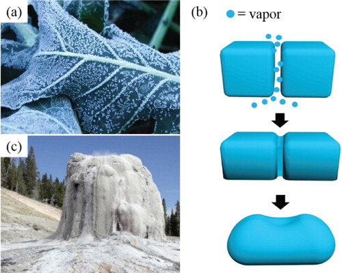
Thermal phase transitions of thermotropic soft matters show various kinds of structures as a function of temperature. Among them, the isotropic liquid to LC phase transition is the most common in LC materials and is known as a clearing point because it does not fully become “solid”. Sublimation is commonly known as a phase transition between the solid to gas phases without passing through the liquid phase, as observed in dry ice (carbon dioxide) at room temperature. More generally, when temperature falls below 0°C in the early morning, gaseous water molecules in air kinetically deposit onto the substrate as observed in frost on plants, in which water vapor-deposition sublimates to frost (Figure (a)). Another example is that slightly separated ice cubes in humid conditions are merged together by sublimation/condensation of nearby water vapor ((b)). Such sublimation/condensation on each surface can be considered as sintering processes, where the term sintering can be broadly defined as a process of compacting, forming, and shaping a solid mass of materials by heat or pressure without melting. For example, sintering occurs naturally in the deposition of minerals [Citation83,Citation84], and geyser cones are occasionally formed as a result of such depositions of incrusted minerals (such as amorphous silica or opaline) near hot springs or petrifying springs, referred to as a “siliceous sinter” ((c)). However, this kind of morphogenesis is not controllable, making it difficult to obtain desired patterns at the micron or nanometer scale during the sintering process.
Figure 5. Sublimation and recondensation in nature (a) Frost on a leaf. (b) Sketches of the process of merging ice cubes in humid conditions. (c) Geyserite at Crater Hills Geyser, formed wherever relatively alkaline hot springs percolate out of the ground.
3.2. Sublimable semi-fluorinated smectic LCs
As an intermediate phase between solid and liquid, the LC phase is commonly composed of supramolecules having molecular weights larger than that of generally sublimable small molecules such as water, carbon dioxide, and naphthalene, meaning that there is a relatively high interactive force between LC molecules preventing sublimation. To control the intermolecular interactions in the LC phase, the substitution of fluorinated groups into supramolecular structures has been extensively studied due to the fascinating properties of such modified species, including their monoatomic nature, high electronegativity, and low polarizability. A very strong carbon-fluorinated (C–F) bond contributes to the high stability of fluoro-substituted compounds [Citation85–87]. In several studies reported by R. E. Banks et al. and P. Kirsch et al., the influence of fluoro-substituents on supramolecular properties was well exemplified compared with normal hydrocarbon compounds and semi-fluorinated carbon compounds [Citation88–90]. The C–F bond is highly polar, but local dipoles are canceled out if the fluorine is symmetrically substituted within the molecular structure, resulting in an overall non-polar system. This low polarizability causes a lower boiling point compared to non-fluorinated molecules and also confers weak intermolecular forces, inducing low surface tension in the liquid state. For example, the fluorinated fullerene, a carbon allotrope with a hollow shape, can be sublimated in contrast to the hydrogenated fullerene which is likely to be degraded rather than sublimated during thermal treatment [Citation91,Citation92]. Therefore, the intrinsic chemical and physical properties of fluorinated groups are important to realize the sublimation and recondensation of supramolecular LC materials.
Recently, it was reported that the sublimation and subsequent recondensation of semi-fluorinated LC materials can occur in the smectic phase of synthetic semi-fluorinated molecules, labeled Y001 to Y006, composed of a rigid biphenyl group with semi-fluorinated alkyl tails ((a)) [Citation67,Citation68]. These molecules show the smectic A phase in a broad temperature range upon cooling from isotropic liquid, and maintain LC structures even after they go to the smectic E phase and into the soft crystal or crystal phase at room temperature (), which is very useful behavior for investigating the nanometer-scale morphology of smectic phases [Citation67]. Similar to other smectics, TFCDs are generated at smectic A phase on the free surface due to the conflicting anchoring conditions, resulting in geometrical depression and cusp-like structures accommodated by the formation of TFCDs, which can be easily observed to show Maltese cross-patterns by polarized optical microscopy (POM) [Citation50,Citation67,Citation68]. The main concept of this work is that the sublimation of semi-fluorinated LC molecules can lead to peeling off of TFCD layers. Meanwhile, LC molecules are re-condensed to reorient perpendicular to the LC/air interface in a local manner, resulting in hierarchical pyramid-like dome structures with hemi-cylindrical decorations made of rolled smectic layers [Citation67].
Figure 6. TGA of LC materials. (a) Chemical structures of Y001–Y006. (b) TGA plots for Y001–Y006 as a function of temperature during heating (heating rate: 1°C/min) shows that sublimation of Y001–Y004 occurs before the material reaches their respective isotropic temperatures; Y005 and Y006 show no sublimation in the SmA phase [Citation68].
![Figure 6. TGA of LC materials. (a) Chemical structures of Y001–Y006. (b) TGA plots for Y001–Y006 as a function of temperature during heating (heating rate: 1°C/min) shows that sublimation of Y001–Y004 occurs before the material reaches their respective isotropic temperatures; Y005 and Y006 show no sublimation in the SmA phase [Citation68].](/cms/asset/a33aa742-e1f5-4d0e-8435-50525b6e8d70/tjid_a_1410500_f0006_c.jpg)
Table 1. Phase transition temperatures of materials during cooling at a rate 5°C/min (Cr = crystal, SmE = smectic E, SmA = smectic A, I = isotropic phase) [Citation68].
To achieve comprehensive understanding and practical use of this unusual LC material phenomenon, the sublimation properties of the LC molecules were analyzed by thermogravimetric analysis (TGA) measurements as a function of temperature while heating at 1°C/min. Based on the TGA plots, mass loss occurs at the smectic A phases of Y001–Y004, meaning that the LC molecules are sublimated or evaporated; the term “sublimation” is used here because the resultant LC textures are more solid than liquid. Y005 and Y006 molecules show mass loss in the isotropic phase over 200°C, which can be considered as evaporation. Increased alkyl chain lengths in the carboxylate groups decrease the sublimation characteristics. The longer aliphatic groups, the more relative polar regions in the molecule, resulting in suppression of thermal sublimation of LC materials.
3.3. Morphological transformation of smectic A phase by sintering
Among synthetic semi-fluorinated LC molecules, Y002 has been studied extensively with regards to its curvatures because this molecule can form large and regular TFCDs. As shown in Figures (a) and (a–c), the layers are of a saddle-like shape with a negative Gaussian curvature, K < 1/(R1·R2) < 0. Each TFCD is smoothly embedded into the surrounding system of flat horizontal layers (K = 0) as the layers cross the cylindrical lateral boundary of the TFCD in a perpendicular fashion. When the smectic film with a hexagonal array of TFCDs is sintered at elevated temperature to reveal the smectic A phase, it experiences dramatic restructuring of its smectic layers. Although a fascinating concept in the morphogenesis of soft matters, such behavior has not been extensively studied. In 2013, Yoon et al. reported that TFCD films can be transformed into a three dimensional layer structure revealing the internal TFCD structure by sintering at 180°C for ∼2 min, during which the uppermost layers are peeled off layer by layer through sublimation and recondensation with anisotropic orientation preferences of the molecules at the free surface [Citation67]. Figure shows POM and SEM images and schematic cross-sectional views for the continuously evolved TFCDs during the sintering process, in which the layers are removed predominantly from the periphery of each TFCD with a progressive loss of birefringence ((a,d,g)). As a result, the final layering structure presents concentric tori patterns with pyramidal dome shapes ((h,i)). The layering-evolution forms many vector edge dislocations at the lateral side of the TFCD on the order of 102 µm during the sintering process, which is caused by layer orientation preferences normal to the solid interface and parallel to the air interface ((f,i)). The internal layers are exposed to the LC/air interface by partial sublimation at the peripheral TFCD regions, creating a new LC/air interface and terminating the deformed layers by rapidly curving down to the solid interface to minimize the energy of the local layer/interface interaction, leading to the conversion of the Gaussian curvature from negative and zero to positive at the nanometer scale. Based on the observations and analysis of the sintered structures, the sublimation and recondensation processes are highly susceptible to sintering temperatures and time, factors that determine the final morphology depending on sublimation and recondensation rate.
Figure 7. Morphology changes of TFCDs during the sintering process. POM textures of TFCD film subject to thermal sublimation at 180°C as a function of time. (a) 0 min, (d) 6 min, (g) 12 min. SEM images of the evolved LC films during sintering and their cross-sectional schemes; (b,c) original TFCDs. (e,f) Dome-like structures. (h,i) Concentric tori patterns with pyramidal dome shape. The film thickness is reduced from ∼5 to <2 µm during the process [Citation67].
![Figure 7. Morphology changes of TFCDs during the sintering process. POM textures of TFCD film subject to thermal sublimation at 180°C as a function of time. (a) 0 min, (d) 6 min, (g) 12 min. SEM images of the evolved LC films during sintering and their cross-sectional schemes; (b,c) original TFCDs. (e,f) Dome-like structures. (h,i) Concentric tori patterns with pyramidal dome shape. The film thickness is reduced from ∼5 to <2 µm during the process [Citation67].](/cms/asset/0ec1aa05-5b42-4e78-8778-3aef72dab245/tjid_a_1410500_f0007_c.jpg)
Very recently, Kim et al. have systematically investigated the morphogenesis of the smectic Y002 film during the sintering process, in which profound changes were observed in terms of the morphology, altering shape, mean, and Gaussian curvature of the layers; this is an improvement over previous reports that only showed a concentric tori pattern with pyramidal dome shapes [Citation67,Citation68]. The emerging structures vary with different sublimation and recondensation rates, much different from the sintered crystalline and amorphous materials and from smectic A textures made under thermal equilibrium conditions.
We will now discuss the general morphological transformations of TFCD films and their reproducibility using sintering diagrams and the corresponding SEM images. These diagrams were constructed with experiments in a temperature range of 130–190°C with a 10°C increment, for different sintering times ranging from 1 to 106 s. Figures and show the resulting diagram, revealing eight distinct types of structures created by sintering: (1) TFCDs with cusp-like depressions at the center, which is similar to the original TFCDs before the sintering process ((m)). All sintered structures passed through this form; (2) TFCDs with spherical caps at the depressions formed at 130–160°C and relatively short sintering times ((n,m,p,s,t)). During cap formation, the uppermost layer of the material first sublimates at different rates within a single TFCD, but condensation is relatively stronger than sublimation within the core of the depression. As a result, the layer ruptures into a curvilinear triangle and then shrinks into a spherical cap by closing up to the depression where the LC molecules are re-condensed from the air, accompanied by diffusion within the smectic A structure. The diffusion only occurs at the core of the central defect where the layered structure of the smectic A phase is broken [Citation68]. (3) Instead of forming spherical caps at the depression, conical pyramids with cusp-like depressions at the defect core ((d–l)) formed at 150–190°C and low-to-moderate sintering times. (4) Conical pyramids with spherical caps at the centers ((q,t)), formed at 130–150°C and low-to-moderate sintering times. The coexistence of (3) and (4) was observed at 150°C (Figures and (n,o)), indicating the transition regime from the cusp to the caps at the defect core. (5) Concentric rings with cusp-like depressions ((i,l,o)), emerged by further sintering of the conical pyramids with cusp-like depressions at high temperatures; (6) concentric rings with spherical caps ((r)), formed from the conical pyramids with spherical caps at low temperatures as the sintering time increases; (7) the spherical caps with central stalks, similar to Udumbara flowers ((u)), emerged at low temperatures (∼130°C) after relatively long sintering times of 105–106 s; further sintering results in disappearance of the stalks and formation of concentric rings at the substrate, with the Udumbara stalk being reduced to a small cap [Citation68]. (8) Domes, formed at 190°C ((a–c)), in which the film loses ∼90% of its volume within less than 1 min of the sintering time, meaning that sublimation is dominant over recondensation.
Figure 8. Sintering diagram of morphological changes of the SmLC films. Eight distinct types of resulting structures as a function of sintering temperatures and times. (1) TFCDs, (2) TFCDs with caps, (3) conical pyramid with depressions, (4) Conical pyramid with caps, (5) concentric patterns with depressions, (6) concentric patterns with caps in centers, (7) Udumbara flower, and (8) Domes. Each structure is marked by a colored box in the diagram and its SEM image is displayed under the diagram [Citation68].
![Figure 8. Sintering diagram of morphological changes of the SmLC films. Eight distinct types of resulting structures as a function of sintering temperatures and times. (1) TFCDs, (2) TFCDs with caps, (3) conical pyramid with depressions, (4) Conical pyramid with caps, (5) concentric patterns with depressions, (6) concentric patterns with caps in centers, (7) Udumbara flower, and (8) Domes. Each structure is marked by a colored box in the diagram and its SEM image is displayed under the diagram [Citation68].](/cms/asset/d6e0807f-a446-4fa9-b860-5c343daa7514/tjid_a_1410500_f0008_c.jpg)
Figure 9. SEM images corresponding to the sintering diagram [Citation68].
![Figure 9. SEM images corresponding to the sintering diagram [Citation68].](/cms/asset/df19ef85-f796-4e8d-a010-92a5d110bb8d/tjid_a_1410500_f0009_c.jpg)
Several morphologies in this diagram are systematically related to each other. For example, during the formation of the Udumbara flower-like structures, its intermediate state (130°C and 80 h) shows a similar structures to the conical pyramids with spherical caps (4) ((q,t)). After sintering for 100 h, LC molecules sublimate from both the conical side surface and the area around the pyramid, resulting in the hemi-tori shrinking into small beads and forming a stalk structure with a spherical cap ((u)). If the sintering exceeds 120 h, these flowers disappear and leave spherical caps in the centers of the TFCDs, which seems to be patterns that form immediately before complete evaporation of the SmA films after prolonged sintering at 130–180°C and concentric rings ((i,l,o,r)).
For all resultant structures, it is noted that sublimation, recondensation, and reconstruction of the layers lead to soaring structures surrounding the cusp of TFCD in (2–4) and (7,8) in ; such features are possibly associated with local vapor pressure within the TFCD along with the curvature of the bending layers. Kim et al. explained the underlying physics of the observed features by relating it to the Kelvin equation, in which the sublimation of molecules is enhanced as a/2 < ρ ≤ a (a is the radius of TFCD and ρ is a normal distance to the defect line, varying along with the surface curvature), and recondensation of molecules is enhanced as 0 < ρ ≤ a/2 ((b)).
Figure 10. Reconstruction of layering in the smectic films during thermal sintering. (a) The mean curvature within the TFCD varies along with ρ from negative inside the cylinder of radius r = a/2 to positive within the region a/2 < r < a. (b) Excess sublimation rate (arbitrary units) versus normalized distance ρ/a from the TFCD axis for three ratio of film thickness (h/a) = 0.5; 1; 2. (c) Harmonious inosculation of equidistant layers between a TFCD remnant with K < 0 and spherical packing system with K > 0. The pair (R1, R2) characterize a point at the smectic layer in spherical cap (R1 = R2) while (,
) corresponds to a point at the layer that is close to vertical axis of rotational symmetry of the TFCD. (d) Inosculation between a TFCD remnant with K < 0 and a hemi-toroidal packing of equidistant smectic layers with K > 0. The toroidal caps with positive Gaussian curvature are pre-Udumbara flower stalks [Citation68].
![Figure 10. Reconstruction of layering in the smectic films during thermal sintering. (a) The mean curvature within the TFCD varies along with ρ from negative inside the cylinder of radius r = a/2 to positive within the region a/2 < r < a. (b) Excess sublimation rate (arbitrary units) versus normalized distance ρ/a from the TFCD axis for three ratio of film thickness (h/a) = 0.5; 1; 2. (c) Harmonious inosculation of equidistant layers between a TFCD remnant with K < 0 and spherical packing system with K > 0. The pair (R1, R2) characterize a point at the smectic layer in spherical cap (R1 = R2) while (, ) corresponds to a point at the layer that is close to vertical axis of rotational symmetry of the TFCD. (d) Inosculation between a TFCD remnant with K < 0 and a hemi-toroidal packing of equidistant smectic layers with K > 0. The toroidal caps with positive Gaussian curvature are pre-Udumbara flower stalks [Citation68].](/cms/asset/9470cf08-55e3-443f-8523-0901b3215666/tjid_a_1410500_f0010_c.jpg)
The experiment demonstrates that there is a preferential molecular orientation perpendicular to the smectic–air interface that induces a Gaussian curvature conversion from negative in TFCDs to positive in the hemi-toroidal (3), (5), (6) and spherical (4), (6–8) structures shown in . The transformed positive Gaussian curvatures with spherical packing are smoothly matched to remnants of the toroidal layers of TFCDs, in which geometry rules that the normal vectors to the SmA layers are straight lines everywhere facilitate the matching between the positive and negative curvatures ((c,d)). This kind of combinative assembly was suggested in 1982 by Sethna and Kleman [Citation93]. Regions of different Gaussian curvatures are separated by interfaces that induce elastic energy. This energy, however, is much smaller than the anisotropic surface anchoring energy gain (see the discussion in [Citation68]). In addition to these sintered structures based on TFCD films, Yoon et al. have also shown nano-sized linear hemi-cylinder patterns using vertically aligned lamella layers prepared using sandwich cells of two glass plates to give planar anchoring forces to the molecules. When one glass plate is removed, a new LC/air interface emerges in which the molecules are normal to the layers, and parallel to the air boundary. Sintering of the sample then leads to formation of linear hemi-cylinders on the order of 102 nm through sublimation and reconstruction [Citation67]. Although Lacaze et al. reported similar hemi-cylinder structures in very thin films of octylcyanobiphenyl on MoS2 (exerting planar anchoring), these hemi-cylinder structures were formed on the micron-scale [Citation94]. As mentioned in Section 2.1, in spite of the formation of TFCDs on the micron-scale, the sintering process develops deviated nano-sized layer structures through the sublimation and recondensation of LC molecules. Accordingly, the morphogenesis of curvatures in smectic LCs during the sintering process is an important indicator that sublimation and recondensation can facilitate a curvature layering on the nanoscale, which is difficult for LC materials when forming bulk curvature on the micron-scale.
4. Applications
4.1. Superhydrophobic surfaces
Superhydrophobic surfaces have been extensively studied due to their self-cleaning applications; one example is in “lotus leaves”, where the most important characteristic is a dual-scale roughness that has coarse-scale feature sizes of around 10–20 µm co-existing with finer structures of 100 nm to 1 µm [Citation95,Citation96]. Soft building blocks such as block copolymers, colloids, and LCs have been attractive in micro-or nanofabrication processes because their self-assembling characteristics facilitating spontaneous and reversible formation of periodic dual-scale structures over a large area [Citation58,Citation97–99].
In 2013, Kim et al. demonstrated the simple fabrication of surfaces with dual roughness by sintering of micro-pillar substrates. In this process, smectic materials are loaded on micro-pillar patterned substrates above the isotropic temperature, followed by cooling to the smectic A phase to generate TFCDs. The defect lines at the TFCD cores were mostly attracted to the pillar edges, inducing the edge-arrangement of TFCDs with the micro-pillars [Citation100]. The samples were then sintered at 140°C for 30 h to generate nano-hemi-cylinders on the micro-pillars (5–10 µm) with a certain film thickness, where the feature size of hemi-cylinder is 100 nm high and 200 nm wide. As result of this process, dual-scale patterns mimicking lotus leaves were successfully formed ((a,b)). The superhydrophobicity of the surface was evaluated by measuring contact angles (CAs) of water droplets. After sintering at 140°C, the CA values of both surfaces were dramatically increased ((c)). In the final step ((d)), nanoscale hemi-cylinders were generated on the pillars, and the CA values reached a maximum of ∼150° with small hysteresis of 9° after 36 h, showing the typical superhydrophobicity of sintered patterns. Based on these results, sintered smectic films on micro-pillars effectively repel water droplets to reduce water-to-substrate contact area, and this system can provide a simple and useful platform to create micro–nano hybrid structures.
Figure 11. Nanoscale hemi-cylinders on micro-patterned substrate and CA measurements on the patterns. (a) The SEM images showing that hemi-cylinders were conformal coated with pillar arrays after thermal sintering at 140°C for 30 h. (b) Magnified SEM images of single micro-pillar (l = 10 µm) clearly showing dual-scale roughness. (c) The plots of CA measurements on the micro-patterns (red line, l = 10 µm and black line, l = 5 µm) as a function of thermal sintering durations. (d–f) SEM images of hierarchically evolved TFCDs on the pattern with l = 10 µm during sintering and each inset is optical image of the water droplet for each state [Citation100]. All scale bars are 10 µm.
![Figure 11. Nanoscale hemi-cylinders on micro-patterned substrate and CA measurements on the patterns. (a) The SEM images showing that hemi-cylinders were conformal coated with pillar arrays after thermal sintering at 140°C for 30 h. (b) Magnified SEM images of single micro-pillar (l = 10 µm) clearly showing dual-scale roughness. (c) The plots of CA measurements on the micro-patterns (red line, l = 10 µm and black line, l = 5 µm) as a function of thermal sintering durations. (d–f) SEM images of hierarchically evolved TFCDs on the pattern with l = 10 µm during sintering and each inset is optical image of the water droplet for each state [Citation100]. All scale bars are 10 µm.](/cms/asset/34e78013-68a5-45f6-8736-90186ff03884/tjid_a_1410500_f0011_c.jpg)
4.2. Nanoparticle clustering arrays
Nanoparticles (NPs) that self-assemble into ordered nanostructures present unusual structural and opto-electric characteristics [Citation101–103]. In particular, creation of periodic and uniform NP cluster (NPC) arrays over large areas is an important interdisciplinary topic in optoelectronics for the purpose of tuneable photonic devices [Citation104,Citation105]. A variety of methods have been described to achieve well-ordered arrays of NPCs, but there is still demand to make processes more simplified and cost-effective.
Recently, it was suggested that periodic array of NPCs can be fabricated over a large area using sublimable smectic materials. On free surfaces, LC materials can produce highly periodic topographical cusp-like patterns of TFCDs, where the cusp-like depressions provide a confinement effect to trap NPs. The NPs in the cusp site are then synergistically assembled into spherical NPCs with morphological changes in the TFCDs during sintering in the smectic A phase, resulting in periodic arrays of NPCs over large areas. Using this method, Kim et al. have demonstrated that in a hexagonal array of quantum dots (QDs) for fluorescent displays, the arrangement of the QD clusters is determined by highly periodic TFCD defect arrays [Citation106]. Fabrication was performed by spin-coating the NP suspension on the TFCD film, followed by sintering at moderate smectic A temperatures. As a proof-of-concept, two kinds of NPs were used, being fluorinated silica NPs (F-SiO2; diameter ∼ 100 nm), and QDs (CdSe/CdS/ZnS, diameter ∼4 nm); these NPs were directly investigated by POM and SEM [Citation106]. After spin-coating of NPs, F-SiO2, clear hexagonal Maltese cross-patterns appear in the SEM images, where NPs were dispersed and irregularly aggregated on the cusp-like depressions of TFCDs ((a,b)). When the NP smectic film was sintered at 160°C, the macroscopic reconstruction to form conical pyramid ((q)) was not found, but concentric ring patterns were generated with LC/NP protrusions in the center of ring patterns after 1–2 h of sintering ((c–f)). After 4 h of sintering, all LC materials were sublimated, leaving only the spherical aggregates of F-SiO2 NPs at the original cusp site of TFCD ((g,h)). This is also observed using POM, showing no birefringence ((g)), which implies complete removal of the LC molecules. The size of the NPC is reduced to ∼ 800 nm, and SEM images clearly show highly ordered NPC arrays (inset of (g)) over a large area (500 × 500 µm2). A series of illustrations show that the layers of the cusp-like depression regions are mixed with NPs, whereas the interconnecting layers between cusps were gradually removed during thermal annealing. Finally, the NPs accumulate together to form NPCs on the substrate without the LC material. A wider arrow denotes a faster sublimation rate in (d,f).
Figure 12. POM and SEM images of the TFCDs top-coated by F-SiO2 NPs during thermal sintering at 160°C and sketches of the cross-section view of the corresponding TFCD. (a, b) The initial state of the TFCDs coated by F-SiO2. (c–f) The images of TFCDs are taken after 1 and 2 h sintering of 160°C, respectively. Layers are sublimed and partially reconstructed to spherically cluster NPs at the defect region of the TFCD but molecular arrangement at peripheral part of TFCDs retains. (g) The POM shows no birefringence after 4 h sintering, meaning that all the LC molecules were evaporated. The inset of (g) and (h) shows the remained NPC without LC material. The illustration shows how the NPs are clustered together into a spherical assembled one as a function of sintering [Citation104].
![Figure 12. POM and SEM images of the TFCDs top-coated by F-SiO2 NPs during thermal sintering at 160°C and sketches of the cross-section view of the corresponding TFCD. (a, b) The initial state of the TFCDs coated by F-SiO2. (c–f) The images of TFCDs are taken after 1 and 2 h sintering of 160°C, respectively. Layers are sublimed and partially reconstructed to spherically cluster NPs at the defect region of the TFCD but molecular arrangement at peripheral part of TFCDs retains. (g) The POM shows no birefringence after 4 h sintering, meaning that all the LC molecules were evaporated. The inset of (g) and (h) shows the remained NPC without LC material. The illustration shows how the NPs are clustered together into a spherical assembled one as a function of sintering [Citation104].](/cms/asset/4d6514ac-c177-4541-b5c9-6b1b61b9e1b1/tjid_a_1410500_f0012_c.jpg)
In this system, the different sublimation rates within a single TFCD play a crucial role in forming NPCs. The fast sublimation rate of the peripheral TFCD region induces topographical differences within the central region, and the NPs on the cusps can effectively block the molecular sublimation at the center region. As results of these factors, the geometry of LC/NPs is much differently evolved from the previous case () during sintering. Thus, the spherical assembly of NPCs is a representative application showing the obvious role of different sublimation and recondensation rates in TFCDs.
4.2.1. Illumination panel
Based on this preliminary result, an illuminating system consisting of a hexagonal array of QDs was fabricated (). The semiconductor QDs present unusual opto-electric properties owing to quantum confinement effects, a promising characteristic for many applications. Although many methods for QD arrays including templating, inkjet printing, and transfer printing have been introduced [Citation107–110], conditions of pre-patterning the templates, low cost, and simple fabrication were not fully satisfied. Accordingly, a hexagonal array of QD clusters was easily fabricated over a large area (500 × 500 µm2) after ∼4 h of sintering via spontaneous assembly of QDs and LC (). The fast Fourier transform (FFT) (inset in ) clearly shows well-ordered QD cluster arrays with hexagonal symmetry. Moreover, it is possible to realize various types of NPC arrays including QD clusters by using the topographical confinement of LCs [Citation48–50,Citation52].
Figure 13. The illumination of QD cluster arrays. A fluorescent microscopy image shows the hexagonal arrays of QD clusters as TFCDs were formed. Inset is two-dimensional FFT image [Citation106].
![Figure 13. The illumination of QD cluster arrays. A fluorescent microscopy image shows the hexagonal arrays of QD clusters as TFCDs were formed. Inset is two-dimensional FFT image [Citation106].](/cms/asset/3071dc8d-284d-45ef-ac9f-98eb2bbfdf32/tjid_a_1410500_f0013_c.jpg)
4.2.2. SERS application
Clustering of gold nanorods (GNRs) leads to extremely high electromagnetic fields that produce enhanced optical signals, facilitating sensing applications. For this application, GNR cluster arrays were fabricated via the approach outlined above and they could be successfully used for SERS. Among the various techniques to assemble GNRs, solution-evaporative assembly has thus far been used extensively [Citation111–113]. However, regular solute assembly on the substrate during solvent evaporation is not easy to manipulate, requiring extremely sensitive experimental conditions. Furthermore, the process is time consuming because the assembly proceeds through thermodynamic processes, where particle–particle, particle–solvent, and suspension–substrate interactions must be considered [Citation111–115]. In contrast, the method based on sublimable LCs only requires surface affinity between the NPs and LC molecules, because the morphological evolution of TFCDs during thermal annealing can effectively make well-arrayed NPCs [Citation116]. In addition, the entire process takes less than 1 h.
The SERS activity of the fluorinated GNR (F-GNR) clusters arrays fabricated using the method was investigated by employing them for the analysis of Malachite green (MG), a typical banned fish pesticide (). For this purpose, two kinds of samples were prepared, with the same amount of F-GNRs in each: (1) monolayer of F-GNRs on a bare silicon wafer, which was prepared by the conventional solvent-evaporation method; and (2) F-GNR clusters prepared by the outlined method. The two kinds of samples were immersed overnight in a 1.0 × 10⁻⁸ M aqueous solution of MG, and then completely dried prior to the SERS measurement. For each SERS experiment, a Raman spectrometer with a probe laser (wavelength = 531 nm) was used. The silicon wafer was used as the bottom substrate, and shows the typical Raman peaks at 450 and 900 cm−1 (green line in (a)), which can be ignored when comparing the two sample types. The spectrum of the arranged GNR clusters (red line in (a)) shows a significant amplification of the peak intensity of the Raman peak at ∼1544 cm−1 when compared to the GNR monolayer (blue line) on Si wafer. The intensity ratio at 1544 cm−1 for the two spectra was calculated to be IR/IB ∼10 (IR is the red line for the F-GNR cluster and IB is the blue line for monolayer F-GNR), indicating that the peak intensity on the F-GNR array was amplified by an order of magnitude compared to the GNR monolayer. This result clearly demonstrates that clustering of GNRs significantly enhances Raman signals compared to unpatterned GNRs. Moreover, the spectrum from the F-GNR array shows the characteristic Raman peaks of MG at the concentration of 1.0 × 10⁻⁸ M, indicating that its SERS performance satisfies the detection limit of 1.0 × 10⁻⁸ M required by the European Commission and the US Food and Drug Administration [Citation111]. This result shows the quite striking cost effectiveness of our platform because the same amount of the nanorod sample was used on both the experiments, despite the large difference between the SERS spectra of the GNR cluster array and the monolayer.
Figure 14. GNR clusters array for SERS application (a) Typical SERS spectra (λex = 531 nm) of MG (1.0 × 10⁻⁸ M) on the GNR cluster array (red), GNR monolayer (blue), and bare silicon substrate (green). (b) Histogram for the SERS intensity at the 1544 cm−1 peak of MG from 20 different GNR clusters, which are indicated in the inset (the scale bar of inset is 5 µm) [Citation116].
![Figure 14. GNR clusters array for SERS application (a) Typical SERS spectra (λex = 531 nm) of MG (1.0 × 10⁻⁸ M) on the GNR cluster array (red), GNR monolayer (blue), and bare silicon substrate (green). (b) Histogram for the SERS intensity at the 1544 cm−1 peak of MG from 20 different GNR clusters, which are indicated in the inset (the scale bar of inset is 5 µm) [Citation116].](/cms/asset/168e8301-561c-4fb7-8ec8-7d1a0f855dc5/tjid_a_1410500_f0014_c.jpg)
For the reproducibility of the SERS performance of the arranged GNR clusters, the laser was focused on each GNR cluster, and the corresponding Raman peak intensities were compared from cluster to cluster. (b) shows the histogram of each SERS intensity at 1544 cm−1 from 20 different GNR clusters (inset of (b)), confirming good reproducibility.
5. Conclusion
In this review, we have discussed the general features and concepts of curvature morphogenesis in SmLC films and TFCDs through sublimation and recondensation phenomena, and its application to the fabrication of micro/nano hybrid patterns as well as assembly of NPCs. The complex morphological changes are related to many contributing mechanisms, such as sublimation rate, that vary with sintering temperature, anisotropic surface energies, bulk elasticity, and anisotropic diffusion of matter. Yoon and Kim et al. have attempted to understand the key observed features based on many sintering experiments and a theoretical approach using the classic Kelvin equation. However, many issues must still be resolved in both experimental and theoretical studies to describe the dynamics of the underlying morphogenesis of the curvatures via sublimation and condensation.
In fact, the thermodynamic term ‘sublimation’ was not associated with supramolecular chemistry because sublimation is unlikely to occur in such highly correlated molecular systems in bulk. Moreover, the conversion of Gaussian curvature from negative to positive is rarely met in equilibrium smectic films with free surface because a positive Gaussian curvature increases the mean curvature and thus a higher energy cost of the layering. Thus, the sublimation and recondensation of the fluorinated SmLC presents a very interesting field encompassing many topics from molecular design to controlling curvature of layers and interfaces in soft matter. Furthermore, this sublimation and recondensation system can be an intelligent solution for several issues in applications of LC defects regarding size reduction on the nanoscale and manipulation of new types of defect orders.
Additional information
Funding
Notes on contributors

Dae Seok Kim
Dae Seok Kim received her B.S. degree in Department of Chemistry from Chungnam National University, Daejeon, South Korea, in 2012, and Ph.D. degree in Graduate School of Nanoscience and Technology (GSNT) from KAIST in 2017. He currently joined in EC2M, UMR 7083 Gulliver of Centre National de la Recherche Scientifique (CNRS) in ESPCI Paris for postdoctoral research and study about functionalization of topological defects of soft matters such as liquid crystals, polymers, and colloids.

Dong Ki Yoon
Dong Ki Yoon received his B.S. degree in chemical engineering from Yonsei University in 2001, and M.S. and Ph.D. degrees in chemical and biomolecular engineering from KAIST in 2003 and 2007, respectively. After working on the next-generation nanofabrication project in Samsung Electronics Co. for 2 years, he joined the Department of Physics at the University of Colorado, Boulder, for his postdoctoral research and focused on the study of the novel phenomena of liquid crystals in marginal space and laser induced defects of liquid crystals. Following this, he joined KAIST as an assistant/associate professor in both the GSNT and department of chemistry in 2011 and 2017, respectively. Currently, he leads ‘Soft Matter nano-Assembly group’ to pioneer the patterning applications based on soft matters such as liquid crystals, supramolecules, and polymers.
References
- S. Förster and M. Konrad, J. Mater. Chem. 13, 2671 (2003). doi: 10.1039/B307512P
- I. Saraogi, C.D. Incarvito and A.D. Hamilton, Angew. Chem. 120, 9837 (2008). doi: 10.1002/ange.200803778
- N. Stoop, R. Lagrange, D. Terwagne, P.M. Reis and J. Dunkel, Nat. Mater. 14, 337 (2015). doi: 10.1038/nmat4202
- T. Kirchhausen, Nat. Cell Biol. 14, 906 (2012). doi: 10.1038/ncb2570
- J. Zimmerberg and M.M. Kozlov, Nat. Rev. Mol. Cell Biol. 7, 9 (2006). doi: 10.1038/nrm1784
- C.C. Conwell, I.D. Vilfan and N.V. Hud, Proc. Natl. Acad. Sci. 100, 9296 (2003).
- G.W. Orr, L.J. Barbour and J.L. Atwood, Science, 285, 1049 (1999). doi: 10.1126/science.285.5430.1049
- R. Parthasarathy and J.T. Groves, Soft Matter 3, 24 (2007). doi: 10.1039/B608631D
- S. Granick, A.L. Demirel, L.L. Cai and J. Peanasky, Isr. J. Chem. 35, 75, (1995). doi: 10.1002/ijch.199500013
- J. Kopeček, Biomaterials 28, 5185 (2007). doi: 10.1016/j.biomaterials.2007.07.044
- J. Genzer and J. Groenewold, Soft Matter. 2, 310 (2006). doi: 10.1039/b516741h
- V. Shenoy and A. Sharma, Phys. Rev. Lett. 86, 119 (2001). doi: 10.1103/PhysRevLett.86.119
- I. Tokarev and S. Minko, Soft Matter. 5, 511 (2009). doi: 10.1039/B813827C
- M.D. Silva, M. Dao, J. Han, C.T. Lim and S. Suresh, MRS Bull. 35, 382 (2010). doi: 10.1557/mrs2010.571
- S.-M. Yang, S.G. Jang, D.-G. Choi, S. Kim and H.K. Yu, Small, 2, 458 (2006). doi: 10.1002/smll.200500390
- T. Thurn-Albrecht, J. Schotter, G.A. Kastle, N. Emley, T. Shibauchi, L. Krusin-Elbaum, K. Guarini, C.T. Black, M.T. Tuominen and T.P. Russell, Science 290, 2126 (2000). doi: 10.1126/science.290.5499.2126
- W.A. Lopes and H.M. Jaeger, Nature 414, 735 (2001). doi: 10.1038/414735a
- Y. Knag, J.J. Walish, T. Gorishnyy and E.L. Thomas, Nat. Mat. 6, 957 (2007). doi: 10.1038/nmat2032
- B.R. Sveinbjörnsson, R.A. Weitekamp, G.M. Miyake, Y. Xia, H.A. Atwater and R.H. Grubbs, Proc. Natl. Acad. Sci. 109, 14332 (2012). doi: 10.1073/pnas.1213055109
- K. Thorkelsson, J.H. Nelson, A.P. Alivisatos and T. Xu, Nano Lett. 13, 4908 (2013). doi: 10.1021/nl402862b
- C. Knorowski and A. Travesset, Europhys. Lett. 100, 56004 (2012). doi: 10.1209/0295-5075/100/56004
- S. Zhang, K.H. Lee, C.D. Frisbie and T.P. Lodge, Macromolecules 44, 940 (2011). doi: 10.1021/ma102435a
- D. Demus, J. Goodby, G.W. Gray, H.-W. Spies, V. Vill, Eds. Handbook of Liquid Crystals (Wiley-VCH, Weinheim, 1998), Vol. 3.
- C. Fong, T. Le and C.J. Drummond, Chem. Soc. Rev. 41, 1297 (2012). doi: 10.1039/C1CS15148G
- G.M. Whitesides and B. Grzybowski, Science 295, 2418 (2002). doi: 10.1126/science.1070821
- T. Kato, N. Mizoshita and K. Kishimoto, Angew. Chem. Int. Ed. 45, 38 (2006). doi: 10.1002/anie.200501384
- M. Kleman and O.D. Lavrentovich, Liquid Crystals 36, 1085 (2009). doi: 10.1080/02678290902814718
- M. Kleman and O.D. Lavrentovich, Soft Matter Physics: An Introduction (Springer, New York, 2003), p. 104.
- Y. Bouligand, C. R. Chimie 11, 281 (2008). doi: 10.1016/j.crci.2007.10.001
- M.W. Matsen and F.S. Bates, Macromolecules 29, 7641 (1996). doi: 10.1021/ma960744q
- S.A. Langer and S.C. Glotzer, Physica A 239, 358 (1997). doi: 10.1016/S0378-4371(97)00030-7
- G.M. Whitesides, J.P. Mathias and C.T. Seto, Science 254, 1312 (1991). doi: 10.1126/science.1962191
- S.J. Woltman, G.D. Jay and G.P. Crawford, Nat. Mater. 6, 929 (2007). doi: 10.1038/nmat2010
- C. Zhou and Z. Yi, Biomaterials 20, 2093 (1999). doi: 10.1016/S0142-9612(99)00080-0
- J.J. Hwang, S.N. Iyer, L.-S. Li, R. Claussen, D.A. Harrington and S.I. Stupp, Proc. Natl. Acad. Sci. 99, 9662 (2002). doi: 10.1073/pnas.152667399
- J.B. Fournier, I. Dozov and G. Durand, Phys. Rev. A 41, 2252 (1990). doi: 10.1103/PhysRevA.41.2252
- O.D. Lavrentovich, Sov. Phys. JETP 64, 984 (1986).
- O.D. Lavrentovich, Mol. Cryst. Liq. Cryst. 151, 417 (1987).
- A. Adamczyk, Mol. Cryst. Liq. Cryst. 170, 53 (1989).
- S.L. Aroraa, P. Palffy-Muhoraya, R.A. Voraab, D.J. Davidb and A.M. Dasguptac, Liquid Crystals 5, 133 (1989). doi: 10.1080/02678298908026356
- R. Pratibha and N.V. Madhusudana, J. Phys. II France 2, 383 (1992). doi: 10.1051/jp2:1992140
- C. Blanc and M. Kleman, Eur. Phys. J. E. 4, 241 (2001). doi: 10.1007/s101890170134
- Y. Iwashita and H. Tanaka, Phys. Rev. Lett. 98, 289 (2007). doi: 10.1103/PhysRevLett.98.145703
- J.B. Fournier and G. Durand, J. Phys. II France 1, 845 (1991). doi: 10.1051/jp2:1991113
- H. Naito, M. Okuda and O.-Y. Zhong-Can, Phys. Rev. E 52, 2095 (1995). doi: 10.1103/PhysRevE.52.2095
- W. Guo and C. Bahr, Phys. Rev. E 79, 273 (2009).
- Y.H. Kim, D.K. Yoon, M.C. Choi, H.S. Jeong, M.W. Kim, O.D. Lavrentovich and H.-T. Jung, Langmuir 25, 1685 (2009). doi: 10.1021/la802870z
- A. Honglawan, D.A. Beller, M. Cavallaro, R.D. Kamien, K.J. Stebe and S. Yang, Adv. Mater. 23, 5519 (2011). doi: 10.1002/adma.201103008
- A. Honglawana, D.A. Beller, M. Cavallaro, Jr., R.D. Kamien, K.J. Stebe and S. Yang, Proc. Natl. Acad. Sci. 110, 34 (2013). doi: 10.1073/pnas.1214708109
- D.K. Yoon, M.C. Choi, Y.H. Kim, M.W. Kim, O.D. Lavrentovich and H.T. Jung, Nat. Mater. 6, 866 (2007). doi: 10.1038/nmat2029
- D.A. Beller, M.A. Gharbi, A. Honglawan, K.J. Stebe, S. Yang and R.D. Kamien, Phys. Rev. X 3, 041026 (2013).
- T. Ohzono, Y. Takenaka and J.-I. Fukuda, Soft Matter 8, 6438 (2012). doi: 10.1039/c2sm25416f
- B. Zappone, C. Meyer, L. Brunoc and E. Lacaze, Soft Matter 8, 4318 (2012). doi: 10.1039/c2sm07207f
- Y.H. Kim, D.K. Yoon, H.S. Jeong, O.D. Lavrentovich and H.-T. Jung, Adv. Funct. Mater. 21, 610 (2011). doi: 10.1002/adfm.201001303
- H.-W. Yoo, Y.H. Kim, J.M. Ok, H.S. Jeong, J.H. Kim, B.S. Son and H.-T. Jung, J. Mater. Chem. C 1, 1434 (2013). doi: 10.1039/c2tc00089j
- L. Wang and Q. Li, Adv. Funct. Mater. 26, 10 (2016). doi: 10.1002/adfm.201502071
- L. Pelliser, M. Manceau, C. Lethiec, D. Coursault, S. Vezzoli, G. Leménager, L. Coolen, M. DeVittorio, F. Pisanello, L. Carbone, A. Maitre, A. Bramati and E. Lacaze, Adv. Funct. Mater. 25, 1719 (2015). doi: 10.1002/adfm.201403331
- Y.H. Kim, D.K. Yoon, H.S. Jeong, J.H. Kim, E.K. Yoon and H.-T. Jung, Adv. Funct. Mater. 19, 3008 (2009). doi: 10.1002/adfm.200901135
- Y.H. Kim, D.K. Yoon, H.S. Jeong and H.-T. Jung, Soft Matter 6, 1426 (2010). doi: 10.1039/b924401h
- Y.H. Kim, J.-O. Lee, H.S. Jeong, J.H. Kim, E.K. Yoon, D.K. Yoon, J.-B. Yoon and H.-T. Jung, Adv. Mater. 22, 2416 (2010). doi: 10.1002/adma.200903728
- Y.H. Kim, H.S. Jeong, J.H. Kim, E.K. Yoon, D.K. Yoon and H.-T. Jung, J. Mater. Chem. 20, 6557 (2010). doi: 10.1039/c0jm00910e
- S.O. Kim, H.H. Solak, M.P. Stoykovich, N.J. Ferrier, J.J. de Pablo and P.F. Nealey, Nature 424, 411 (2003). doi: 10.1038/nature01775
- E. Kim, H. Ahn, S. Park, H. Lee, M. Lee, S. Lee, T. Kim, E.-A. Kwak, J.H. Lee, X. Lei, J. Huh, J. Bang, B. Lee and D.Y. Ryu, ACS Nano. 7, 1952 (2013). doi: 10.1021/nn3051264
- I. Bita, J.K.W. Yang, Y.S. Jung, C.A. Ross, E.L. Thomas and K.K. Berggren, Science 321, 939 (2008). doi: 10.1126/science.1159352
- R. Ruiz, H. Kang, F.A. Detcheverry, E. Dobisz, D.S. Kercher, T.R. Albrecht, J.J. de Pablo, P.F. Nealey, Science 321, 936 (2008). doi: 10.1126/science.1157626
- H. Arora, P. Du, K.W. Tan, J.K. Hyun, J. Grazul, H.L. Xin, D.A. Muller, M.O. Thompson, U. Wiesner, Science 330, 214 (2010). doi: 10.1126/science.1193369
- D.K. Yoon, Y.H. Kim, D.S. Kim, S.D. Oh, I.I. Smalyukh, N.A. Clark and H.-T. Jung, Proc. Natl. Acad. Sci. 110, 19263 (2013). doi: 10.1073/pnas.1317922110
- D.S. Kim, Y.J. Cha, M.H. Kim, O.D. Lavrentovich, D.K. Yoon, Nat. Comm. 7, 10236 (2016). doi: 10.1038/ncomms10236
- G.W. Grey and J.W.G. Goodby, Smectic Liquid Crystals: Textures and Structures (Leonad Hill, Glasgow, 1984), p. 97.
- L. Bourdon, J. Sommeria and M. Kleman, J. Phys. France 43, 77 (1982). doi: 10.1051/jphys:0198200430107700
- P.G. de Gennes and J. Prost, The Physics of Liquid Crystals (Clarendon Press, Oxford, 1993), p. 52.
- H. Takezoe and Y. Takanishi, Jpn. J. Appl. Phys. 45, 597 (2006). doi: 10.1143/JJAP.45.597
- L.E. Hough, M. Spannuth, M. Nakata, D.A. Coleman, C.D. Jones, G. Dantlgraber, C. Tschierske, J. Watanabe, E. Körblova, D.M. Walba, J.E. Maclennan, M.A. Glaser and N.A. Clark, Science 325, 452 (2009). doi: 10.1126/science.1170028
- D.R. Link, G. Natale, R. Shao, J.E. Maclennan, N.A. Clark, E. Körblova, D.M. Walba, Science 278, 1924 (1997). doi: 10.1126/science.278.5345.1924
- K. Yamada, S. Kang, K. Takimoto, M. Hattori, K. Shirata, S. Kawauchi, K. Deguchi, T. Shimizu and J. Watanabe, J. Phys. Chem. B 117, 6830 (2013). doi: 10.1021/jp402237y
- L.E. Hough, H.T. Jung, D. Krüerke, M.S. Heberling, M. Nakata, C.D. Jones, D. Chen, D.R. Link, J. Zasadzinski, G. Heppke, J.P. Rabe, W. Stocker, E. Körblova, D.M. Walba, M.A. Glaser, N.A. Clark, Science 325, 456 (2009). doi: 10.1126/science.1170027
- H. Kim, S. Lee, T.J. Shin, E. Korblova, D.M. Walba, N.A. Clark, S.B. Lee and D.K. Yoon, Proc. Natl. Acad. Sci. 111, 14342 (2014). doi: 10.1073/pnas.1414840111
- Ph. Boltenhagen, O.D. Lavrentovich and M. Kleman, Phys. Rev. A 46, R1743 (1992). doi: 10.1103/PhysRevA.46.R1743
- P. Sierro and D. Roux, Phys. Rev. Lett. 78, 1496 (1997). doi: 10.1103/PhysRevLett.78.1496
- R. Bidaux, N. Boccara, G. Sarma, L. de Seze, P.G. de Gennes and O. Parodi, J. Phys. France 34, 661 (1973). doi: 10.1051/jphys:01973003407066100
- C. Meyer, L.L. Cunff, M. Belloul and G. Foyart, Materials, 2, 499 (2009). doi: 10.3390/ma2020499
- M. Kleman, J. Phys. France 38, 1511 (1977). doi: 10.1051/jphys:0197700380120151100
- B.Y. Lynne, K.A. Campbell, J. Moore and P.R.L. Browne, Sediment. Geol. 210, 111 (2008). doi: 10.1016/j.sedgeo.2008.07.006
- J.D. Rimstidt and D.R. Cole, Am. J. Sci. 283, 861 (1983). doi: 10.2475/ajs.283.8.861
- M. Hird, Chem. Soc. Rev. 36, 2070 (2007). doi: 10.1039/b610738a
- V. Percec, M. Glodde, T.K. Bera, Y. Miura, I. Shiyanovskaya, K.D. Singer, V.S.K. Balagurusamy, P.A. Heiney, I. Schnell, A. Rapp, H.-W. Spiess, S.D. Hudsonk and H. Duan, Nature 417, 384 (2002). doi: 10.1038/nature01072
- D.A. Tomalia, Nat. Mater. 2, 711 (2003). doi: 10.1038/nmat1004
- R.E. Banks, Fluorine Chemistry at the Millennium (Elsevier, Oxford, 2000), p. 72.
- R.E. Banks, B.E. Smart and J.C. Tatlow, Organofluorine Chemistry: Principles and Commercial Applications (Plenum Press, New York, 1994), p. 118.
- P. Kirsch, Modern Fluoroorganic Chemistry (Wiley-VCH, Weinheim, 2004), p. 66.
- O.V. Boltalina, V.Y. Markov, A.Y. Borschevskiy, L.N. Sidorov and A. Popovich, Mendeleev Commun. 6, 253 (1996). doi: 10.1070/MC1996v006n06ABEH000749
- O.V. Boltalina, V. Yu, A. Markov, Ya. Borschevskii, N.A. Galeva and L.N. Sidorov, J. Phys. Chem. B 103, 3828 (1999). doi: 10.1021/jp983786k
- J.P. Sethna, Phys. Rev. A 26, 3037 (1982). doi: 10.1103/PhysRevA.26.3037
- B. Zappone, E. Lacaze, H. Hayeb, M. Goldmann, N. Boudet, P. Barois and M. Alba, Soft Matter 7, 1161 (2011). doi: 10.1039/C0SM00747A
- L. Feng, S. Li, Y. Li, H. Li, L. Zhang, J. Zhai, Y. Song, B. Liu, L. Jiang and D. Zhu, Adv. Mater. 14, 1857 (2002). doi: 10.1002/adma.200290020
- T. Nakanishi, T. Michinobu, K. Yoshida, N. Shirahata, K. Ariga, H. Möhwald and D.G. Kurth, Adv. Mater. 20, 443 (2008). doi: 10.1002/adma.200701537
- J.Y. Cheng, A.M. Mayes and C.A. Ross, Nat. Mater. 3, 823 (2004). doi: 10.1038/nmat1211
- G. Zhang, D. Wang, Z.-Z. Gu and H. Möhwald, Langmuir 21, 9143 (2005). doi: 10.1021/la0511945
- H. Kim, Y. Yi, D. Chen, E. Korblova, D.M. Walba, N.A. Clark and D.K. Yoon, Soft Matter 9, 2793 (2013). doi: 10.1039/c3sm27221d
- D.S. Kim, Y.J. Cha, H. Kim, M.H. Kim, Y.H. Kim and D.K. Yoon, RSC Adv. 4, 26946 (2014). doi: 10.1039/C4RA03005B
- S.M. Spillane, T.J. Kippenberg and K.J. Vahala, Nature 415, 621 (2002). doi: 10.1038/415621a
- J.A. Fan, C. Wu, K. Bao, J. Bao, R. Bardhan, N.J. Halas, V.N. Manoharan, P. Nordlander, G. Shvets and F. Capasso, Science 328, 1135 (2010). doi: 10.1126/science.1187949
- J. Lacava, P. Born and T. Kraus, Nano Lett. 12, 3279 (2012). doi: 10.1021/nl3013659
- B. Yan, A. Thubagere, W.R. Premasiri, L.D. Ziegler, L.D. Negro and B.M. Reinhard, ACS Nano 3, 1190 (2009). doi: 10.1021/nn800836f
- A. Gopinath, S.V. Boriskina, N.-N. Feng, B.M. Reinhard and L.D. Negro, Nano Lett. 8, 2423 (2008). doi: 10.1021/nl8013692
- D.S. Kim, A. Honglawan, K. Kim, M.H. Kim, S. Jeong, S. Yang and D.K. Yoon, J. Mater. Chem. C 3, 4598 (2015). doi: 10.1039/C5TC00687B
- W. Cheng, N. Park, M.T. Walter, M.R. Hartman and D. Luo, Nat. Nanotech. 3, 682 (2008). doi: 10.1038/nnano.2008.279
- V. Wood, M.J. Panzer, J. Chen, M.S. Bradley, J.E. Halpert, M.G. Bawendi and V. Bulovic, Adv. Mater. 21, 2151 (2009). doi: 10.1002/adma.200803256
- C.B. Murray, C.R. Kagan and M.G. Bawendi, Annu. Rev. Mater. Sci. 30, 545 (2000). doi: 10.1146/annurev.matsci.30.1.545
- T.-H. Kim, K.-S. Cho, E.K. Lee, S.J. Lee, J. Chae, J.W. Kim, D.H. Kim, J.-Y. Kwon, G. Amaratunga, S.Y. Lee, B.L. Choi, Y. Kuk, J.M. Kim and K. Kim, Nat. Photon. 5, 176 (2011). doi: 10.1038/nphoton.2011.12
- J.K. Stolarczyk, A. Deak, D.F. Brougham, Adv. Mater. 28, 5400 (2016). doi: 10.1002/adma.201505350
- P. Li, Y. Li, Z.-K. Zhou, S. Tang, X.-F. Yu, S. Xiao, Z. Wu, Q. Xiao, Y. Zhao, H. Wang, P.K. Chu, Adv. Mater. 28, 2511 (2016). doi: 10.1002/adma.201505617
- E. Rabani, D.R. Reichman, P.L. Geissler, L.E. Brus, Nature 426, 271 (2003). doi: 10.1038/nature02087
- V.R. Dugyala, M.G. Basavaraj, Langmuir 30, 8680 (2014). doi: 10.1021/la500803h
- Y.-F. Li, Y.-J. Sheng, H.-K. Tsao, Langmuir 29, 7802 (2013). doi: 10.1021/la400948e
- D.S. Kim, A. Honglawan, S. Yang, D.K. Yoon, ACS Appl. Mater. Interfaces. 9, 7787 (2017). doi: 10.1021/acsami.6b15343