
Abstract
Al2O3 films have long been widely used as inorganic encapsulation or passivation layers. The Al2O3 single layer, however, exhibits not only a relatively low barrier performance but also poor environmental stability under harsh conditions due to its hydrolysis reaction with water vapor. Thus, to further improve its environmental reliability and barrier performance as a gas diffusion barrier (GDB), the GDB should be newly designed by forming a nanolaminate structure with ultra-thin sublayers. In addition, through the use of a multilayer based on nanolaminate/organic layers, the nanolaminate film can be effectively protected by a SiO2-inserted organic layer. In this study, alternately stacked nanolaminate/silane-based organic layers are proposed. The nanolaminate-based multilayer achieved a water vapor transmission rate (WVTR) of 5.94 × 10⁻⁵ g/m2/day under 60°C/90% accelerated conditions. In addition, after a bending test, the nanolaminate-based multilayer showed a WVTR increase by a magnitude of one order under a 0.63% bending strain. The proposed environmentally and mechanically stable hybrid thin-film encapsulation offers a strong potential for the realization of washable, wearable, or flexible displays in the future.
1. Introduction
Transparent flexible organic light-emitting diodes (TFOLEDs) are currently considered a next-generation display that will not only revolutionize the current display industry but will also create various free-form displays. A thin-film encapsulation (TFE) process should be applied above and below OLEDs to protect devices on flexible substrates composed of highly reactive organic and metal films from exposure to the factors in the external environment, such as ultraviolet (UV) light, dust, moisture, and oxygen [Citation1–3]. In general, the barrier requirements for encapsulation are less than 10−6 g/m2/day water vapor transmission rate (WVTR) and a 10−3 cc/m2/day oxygen transmission rate to reach a minimum OLED lifetime of 10,000 h [Citation4]. One of the major difficulties in the realization of TFOLEDs, however, has been the absence of impermeable and flexible TFE [Citation5,Citation6]. Therefore, for application as a TFE for TFOLEDs, beyond the conventional rigid glass encapsulation, flexible encapsulation consisting of flexible thin films is required.
Vitex proposed a TFE technology using an inorganic/organic multilayer for flexible TFE; this is known as the Barix™ technology [Citation1,Citation7,Citation8]. The previously reported TFEs have been demonstrated to induce barrier performance and long lifetime for OLEDs, comparable to that achieved with glass encapsulation [Citation1,Citation6]. In particular, atomic layer deposition (ALD)-based TFEs have made it possible to guarantee a long lifetime and an excellent barrier performance at low temperatures of less than 100°C without OLED degradation [Citation9,Citation10]. Al2O3 ALD films have been used for organic electronics as a gas diffusion barrier (GDB) due to their good barrier performance at a low temperature of less than 100°C for multilayers based on inorganic/organic layers [Citation2,Citation5,Citation11,Citation12]. Han et al. reported multilayers based on Al2O3/organic layers as a flexible TFE [Citation11]. In addition, Kwon et al. reported heat-transferable TFE combining Al2O3, Ag, and organic layers [Citation5]. In spite of the usefulness of Al2O3 as a GDB, however, there have been many reports of the corrosion of Al2O3 films in harsh environments [Citation13–15]. Also, Al2O3 ALD films do not show good reliability as a result of the degradation of the film quality due to hydrolysis, resulting in poor barrier performances [Citation2,Citation5]. Therefore, to improve the environmental stability of Al2O3 films, the nanolaminate (NL) system has been introduced for the formation of aluminate phases at the interfaces between ultra-thin Al2O3 sublayers and other sublayers [Citation2,Citation12,Citation14,Citation16]. Chemically stable aluminate phases make the GDB more environmentally reliable and stable against water vapor and oxygen.
Using MgO and ZnO ALD films as GDBs has been proven to be difficult due to their poor barrier properties resulting from their crystallinity [Citation2]. The NL system, however, enables the ALD film to inhibit crystal growth with an increase in thickness [Citation17]. MgO ALD films have good water absorption ability, and aluminate phases form at the interfaces, resulting in the corrosion inhibition of the Al2O3 film. Moreover, ZnO ALD films have a high density and a low elastic modulus [Citation17–19]. The NL system designed with synergistic effects among Al2O3, MgO, and ZnO can be used as an impermeable and flexible GDB for TFOLEDs.
Demonstrated in this study is a highly stable, impermeable, and flexible hybrid TFE layer formed by combining an NL-based GDB and a silane-based polymer (silamer) layer. The proposed functional GDB film has a multi-period NL structure with respective 2-nm-thick sublayers forming a sequential ZnO/Al2O3/MgO (ZAM) unit structure in one period. The 30-nm-thick ZAM NL film exhibited a better barrier performance than the Al2O3 film with an identical thickness, and a multilayer was fabricated based on ZAM/silamer to improve the barrier performance, mechanical flexibility, and environmental stability. The multilayer showed little WVTR change in a bending test with a 10 mm radius. In addition, the silamer layers effectively protected the ZAM NL against harsh conditions, resulting in a WVTR value of 5.94 × 10⁻⁵ g/m2/day under 60°C/90% accelerated conditions.
2. Experiment
2.1. Fabrication of NL and organic layers
Prior to the ALD film deposition, the PET substrate was cleaned with acetone, isopropyl alcohol, and de-ionized water in an ultrasonic sonicator. The ZAM NL film was then deposited using thermal ALD at a low temperature of 70°C (Lucida D 100, NCD). Al2O3, ZnO, and MgO films were deposited by chemically reacting precursors of trimethylaluminum, dimethylzinc (DEZ), and bis-ethyl-cyclopentadienyl-magnesium (Mg(EtCp)2) with an H2O reactant. The ALD chamber was continuously purged with a 50 sccm flow of nitrogen (N2) gas after source exposures, and was then maintained at a base pressure of 0.33 Torr. The growth rates of Al2O3, ZnO, and MgO at a chamber temperature of 70°C were 0.85, 1.00, and 1.03 Å/cycle, respectively; the purge time and precursor exposure times were 10 and 0.2 s in the cases of Al2O3 and ZnO. The Mg(EtCp)2 precursor for MgO deposition was heated at 90°C for easy vaporization; assist pulses of 0.3 s consisting of N2 were additionally used to thoroughly drag the Mg(EtCp)2 out of the canister. The pulse and purge time for Mg(EtCp)2 were 0.8 and 15 s, respectively.
The organic–inorganic hybrid layer based on tetraethoxy silane synthesized by the sol–gel method, named ‘silamer’ in this paper, was thermally cured at 70°C under 5 × 10⁻² Torr for 10 min, resulting in a three-dimensional SiO2-embedded organic layer. The 1-µm-thick silamer layer was spin-coated using an acceleration period of 30 s and a maintenance period of 3 s for 5000 rpm.
2.2. WVTR measurement using the Ca test
The electrical calcium (Ca) test is an effective method of comparing the WVTR values of barrier films [Citation20]. The conductive Ca layer is easily oxidized by the water vapor and oxygen penetrating the barrier film, resulting in the real-time change of resistance over time. Therefore, the WVTR values are calculated using the initial resistance and the resistance change of the Ca layer.
2.3. TEM and EDS analysis
Transmission electron microscopy (TEM) images of the cross-section of the TFE structure were obtained using cs-TEM, and then energy-dispersive spectroscopy (EDS) measurements were carried out for elemental analysis.
2.4. Fluorescent blue OLED fabrication
To demonstrate the applicability to OLEDs, fluorescent OLEDs (FOLEDs) with a structure of indium tin oxide (ITO, 150 nm) as an anode, HAT-CN (5 nm) as a hole injection layer, N,N0-di-1-naphthyl-N,N0-diphenylbenzidine (NPB, 45 nm) as a hole transport layer, 2-methyl-9,10-di(2-naphthyl)anthracene (MADN):p-bis(p-N,N-di-phenyl-aminostyryl) (DSA-ph) (25 nm, 3%) as an emission layer, tris(8-hydroxyquinoline) aluminum (Alq3, 10 nm) as an electron transport layer, lithium quinolate (Liq, 1 nm) as an electron injection layer, and Al (100 nm) as a cathode were fabricated using thermal evaporation. Before and after the TFE application, the electro-optical characteristics of the OLEDs were measured.
3. Results and discussion
3.1. GDB properties and environmental stability of the ZAM NL and hybrid multilayer
Before the ZAM NL structure was used as an inorganic layer, the ZAM NL structure was optimized according to the sublayer thickness. As each sublayer had a different ALD growth rate, the sublayer thicknesses were controlled by the cyclic ratios of ZnO:Al2O3:MgO. (a) shows the WVTR values of the approximately 50-nm-thick ZAM NL film with a variation of the sublayer thickness. The sublayer thicknesses were varied as 0.25, 0.5, 2, 5, 10, and 17 nm, where increasing the sublayer thickness means decreasing the number of interfaces between the sublayers. The interfaces in NL structures work as effective diffusion barriers against water vapor and oxygen. In the ZAM NL structure, the Al2O3 sublayers work as a key GDB to obtain an excellent barrier performance (Figure S1). The ZM NL film, which does not contain Al2O3 sublayers, showed much poorer barrier performance than the ZAM NL film. Therefore, although the NL structure helps improve the barrier performance of the barrier film, the Al2O3 sublayer is required as a key GDB for a highly impermeable NL film. In particular, the Al2O3 sublayers chemically react at the interfaces with the MgO and ZnO sublayers. The chemical reaction forms aluminate phases such as Al-Mg-O and Al-Zn-O bonding. Due to the aluminate phases, the ZAM NL becomes densely packed and environmentally stable. On the other hand, the ZnO/MgO (ZM) NL structure without Al2O3 sublayers exhibited a poor barrier performance. Therefore, although the Al2O3 ALD single layer showed a corrosion problem under a harsh environment, the Al2O3 sublayers should be used for impermeable and stable NL fabrication. The proposed ZAM NL films were designed to improve the barrier performance, environmental stability, and flexibility through the synergistic combination of the sublayers. The proposed ZAM NL structure was a defect-decoupling and multi-interfacial film consisting of ZnO, Al2O3, and MgO sublayers. The GDB properties of the ZAM film and the ZAM-based multilayer were evaluated using a Ca test. (b) shows the Ca test results of the various barrier structures. The amorphous Al2O3 film, compared to the MgO and ZnO films, showed better barrier properties for a 30-nm-thick film under 30°C/90%. When the Al2O3 film was kept in a harsher environment of 60°C/90%, however, the barrier performance of the Al2O3 film was rapidly degraded due to the accelerated hydrolysis. On the other hand, the proposed ZAM NL film exhibited improved barrier properties compared to the Al2O3 film. This improvement is attributed to the multi-interfacial and defect-decoupling effects induced by the introduction of the NL system, resulting in chemical bonding at the interfaces between the sublayers. In addition, the NL structure reduces the dependency on Al2O3 in the GDB. Therefore, the NL-based GDB is very effective for fabricating highly impermeable and stable TFE.
Figure 1. (a) WVTR values according to the sublayer thickness under 30°C/90% RH. (b) Ca test results of the 30-nm-thick ZAM and Al2O3 films under 30°C/90% and 60°C/90% RH, respectively. AFM images of (c) PET and (d) PET/silamer. (e) Surface roughness and peak-to-valley surface roughness values of the layers deposited on a PET substrate. (f) Normalized conductance curves vs. time of the ZAM, ZAM/silamer, 1.5-dyad ZAM/silamer, and 2.5-dyad ZAM/silamer structures.
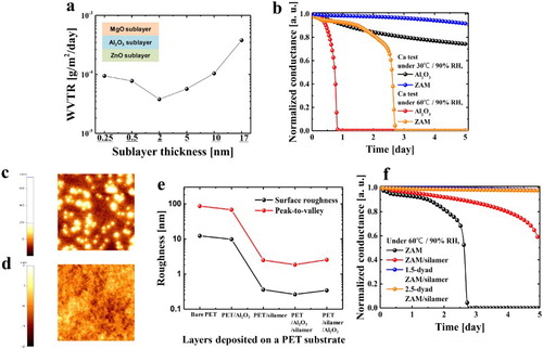
To fabricate a more moisture-resistant, stable, and flexible TFE, organic–inorganic hybrid layers were introduced between the ZAM NL films. In general, the bare PET surface was very rough, and hence, it was difficult to directly fabricate the organic electronic devices thereon. Therefore, for stable and reliable device fabrication, the PET surface should be planarized by a planarization layer. (c,d) shows the atomic force microscope images of the PET surfaces before and after planarization. The PET surface with high surface roughness and peak-to-valley values was smoothed by a 1-µm-thick silamer layer. In addition, the change in the PET surface roughness resulting from the formation of layers was investigated ((e)). Although the ALD system deposits a uniform ALD film, the condition of the surface to be formed is very important. From the measurement results, the bare PET and PET/Al2O3 showed little differences in surface roughness. The coating of the silamer layer, however, reduced the surface roughness to less than 1 nm, resulting in a defect-free and uniform ALD film in forming the multilayer system.
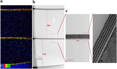
Furthermore, the silamer works not only as a planarization layer but also as a protective layer against harsh environmental conditions. Although the silamer layer showed a poor barrier performance of 10−1 g/m2/day in this study, it effectively inhibited the degradation of the inorganic layer as a capping layer. (f) shows the Ca test results with an increasing number of layers for the multilayers. The introduction of a silamer layer on the ZAM NL film improved the environmental stability, resulting in a significant decrease in the WVTR. In addition, the 1.5- and 2.5-dyad multilayers based on ZAM/silamer exhibited a better barrier performance or barrier performance comparable to that of the best reported TFEs based on Al2O3, MgO, Al2O3/TiO2 nanolaminates, etc. [Citation5,Citation6,Citation13]. The fabricated 2.5-dyad Al2O3 (30 nm)/silamer (1 µm) multilayer is shown in . The cross-sectional TEM and EDS images show that the ZnO, Al2O3, and MgO sublayers are formed separately in the ZAM NL film.
Figure 2. (a) Elemental analysis and (b) cross-sectional TEM images of the 2.5-dyad ZAM/silamer multilayer formed on a Si wafer. (c) Enlarged TEM image of the ZAM NL film (inset: enlarged TEM images of the ZAM NL films in scale).
3.2. Evaluation of the mechanical properties of the hybrid multilayer
The mechanical properties of TFE layers are important for reliable and flexible TFE application to TFOLEDs. In particular, although the Al2O3 ALD films are the most studied GDB films for various applications, they cannot withstand high bending stress due to their brittleness [Citation21]. To improve the limited flexibility of the Al2O3 film, the NL structure provides a good solution. The mechanical properties of the ZAM NL film and multilayer were investigated through a comparison of the nanoindentation and WVTR results before and after bending. First, the hardness and elastic modulus of the Al2O3, ZAM, and silamer layers were measured, as shown in (a). The hardness (H) and the elastic modulus (E) of the ZAM NL films with sublayer thickness variation were obtained to investigate the correlation between the sublayer thickness and the mechanical properties. The E values of the Al2O3 and ZAM NL films with a 2 nm sublayer thickness were 134.36 and 82.7 GPa, respectively, and the H values were 8.58 and 6.25 GPa. The E and H values of the ZAM NL film tended to decrease with a decrease in sublayer thickness. The decreasing elastic modulus and hardness are attributed to the structural transition from the nanocrystalline to amorphous nature of the ZnO and MgO sublayers [Citation18]. In general, the Al2O3 ALD films have an amorphous state, and the ZnO and MgO ALD films show crystalline growth with an increase in thickness [Citation2,Citation5]. Therefore, the sublayer thickness of the ZnO and MgO films mainly affects the E and H values in the ZAM NL film. The ZAM film with a 2 nm sublayer thickness exhibited significantly improved mechanical properties. A softer multi-stacking structure compared to the Al2O3 single layer, consisting of ultra-thin sublayers, was realized with the ALD system, through structural control. In addition, the E and H values of the silamer layer (1.8 and 0.1 GPa, respectively) were much lower than those of the ZAM NL film. Therefore, the mechanical reliability of the multilayer structure with a different modulus of elasticity between the two materials can be enhanced [Citation22].
Figure 3. (a) Elastic modulus and hardness values of the Al2O3, ZAM, and silamer layers (inset: elastic modulus and hardness values of silamer). (b) Changes in the WVTR values of the 2.5-dyad ZAM/silamer and 2.5-dyad Al2O3/silamer multilayers before and after the bending tests with 0.63% bending strain. (c) WVTR values of the 2.5-dyad ZAM/silamer multilayer after the bending tests as a function of the bending strain (0% strain means the unbent multilayer).
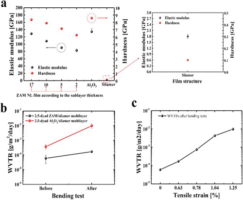
In addition, the WVTR change was evaluated through the measurement of the WVTR values of the thin films before and after the bending tests. Bending tests with tensile strain were conducted to compare the mechanical reliability of the 2.5-dyad ZAM/silamer multilayer with that of the 2.5-dyad Al2O3/silamer multilayer ((b)). The WVTR value of the 2.5-dyad ZAM/silamer multilayer changed slightly within a magnitude of one order before and after the bending test with a 1 cm bending radius, corresponding to 0.63% strain. In contrast, the 2.5-dyad Al2O3/silamer multilayer showed a significant increase in WVTR due to the cracking in the Al2O3 film. This consequent difference shows that an NL structure can be introduced to overcome the brittleness of the oxide single layer, achieving improved flexibility due to the reduced elastic modulus resulting from the formation of multi-stacked sublayers. In addition, the WVTR values of the 2.5-dyad ZAM/silamer multilayer as a function of the bending strain are shown in (c) to investigate the critical strain, and a significant increase in WVTR can be observed. The WVTR of the bent 2.5-dyad ZAM/silamer at a bending strain of more than 1% was two orders of magnitude higher than that of the unbent ZAM-based multilayer due to the cracking of the ZAM NL film. In other words, a threshold for the onset of crack formation can be determined at a critical strain of about 1.0%. This mechanical stability is comparable to the critical strain reported for other TFEs.
Therefore, the structurally designed ZAM-based multilayer showed an excellent barrier performance and mechanical stability suitable for TFOLEDs.
3.3. Electrical-optical characteristics of the thin-film-encapsulated blue OLED
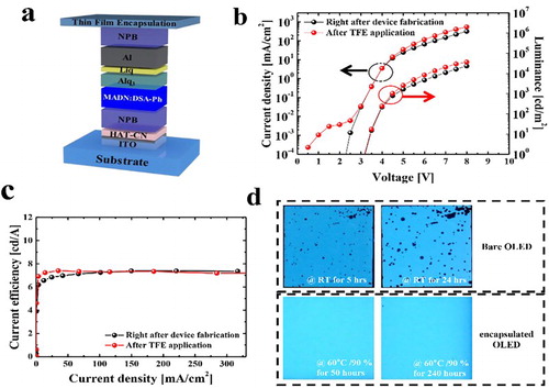
To demonstrate the feasibility of the ZAM-based multilayer, a blue OLED was fabricated on an ITO-coated glass substrate, and was then passivated with TFE ((a)). To evaluate the process reliability and barrier properties induced by the passivation of the ZAM-based multilayer, the current density–voltage–luminance (J–V–L) characteristics of the bare and encapsulated OLEDs were measured. The OLED device did not show performance degradation after the encapsulation process to form TFE consisting of Al2O3 and silamer layers, presenting almost identical J–V–L characteristics ((b,c)). In other words, the process temperature and materials for the formation of the ZAM and silamer layers did not damage the performance of the OLED devices. The FOLEDs had a turn-on voltage of around 3.2 V, a maximum luminance of 36649 cd/m2, and a maximum efficiency of 7.38 cd/A. To investigate the passivation effect of the ZAM NL film, the cell images of the unencapsulated and encapsulated FOLEDs obtained over time were observed. As shown in (d), in the case of the unencapsulated FOLED stored at room temperature, many dark spots were generated by the penetrating water vapor and oxygen within a few hours. On the other hand, although the FOLED encapsulated with the effective TFE was exposed to a harsh environment of 60°C/90% for 240 h, its cell image was almost clear. Therefore, the ZAM-based multilayer film showed good potential as a TFE for practical application to OLED devices.
Figure 4. (a) Schematic structure of blue-emitting FOLEDs. (b) J–V–L characteristics of FOLEDs before and after TFE to OLEDs. (c) Current efficiency vs. current density. (d) Cell images of bare and encapsulated OLEDs under 60°C/90% conditions.
4. Conclusion
In summary, the ZnO/Al2O3/MgO nanolaminate (ZAM NL) films formed with alternating 2-nm-thick ZnO, Al2O3, and MgO sublayers using ALD exhibited significantly improved barrier properties and environmental stability compared to the Al2O3 film. In addition, a 1-µm-thick silane-based inorganic/organic hybrid layer helped protect the ZAM film upon exposure to harsh conditions of 60°C/90%, and effectively planarized the rough PET surface, providing less than 0.4 nm surface roughness and less than 3 nm peak-to-valley values. The 2.5-dyad ZAM/silamer multilayer exhibited a very low WVTR value of 5.94 × 10⁻⁵ g/m2/day and good mechanical stability under 0.63% strain, as measured through an electrical calcium (Ca) test and a bending test. In addition, the proposed multilayer showed stable electrical-optical characteristics after TFE application to an OLED, without performance degradation. Therefore, after further work towards practical application, the proposed TFE layer is expected to be a viable candidate for use as a water-resistant, impermeable, and flexible encapsulation technology in transparent, flexible, and wearable displays based on organic electronics.
Supplemental Material
Download MS Word (72 KB)Disclosure statement
No potential conflict of interest was reported by the authors.
Additional information
Funding
Notes on contributors

Jeong Hyun Kwon
Jeong Hyun Kwon received his B.S. degree in electrical engineering from Hanyang University, Seoul, South Korea in 2013, and his M.S. degree from Korea Advanced Institute of Science and Technology (KAIST), Daejeon, South Korea in 2015. He is currently pursuing his Ph.D. degree in KAIST. His current research interests include thin-film encapsulation (TFE) for flexible and transparent OLEDs.

Yongmin Jeon
Yongmin Jeon, received his B.S. degree in information display from Kyung Hee University, Seoul, South Korea in 2015, and his M.S. degree in electrical engineering from KAIST in 2017. He is currently a Ph.D. candidate in KAIST. His major field of research is flexible OLEDs and its medical applications.

Seungyeop Choi
Seungyeop Choi received his B.S. degree in information display from Kyung Hee University in 2014, and his M.S. degree in electrical engineering from KAIST in 2016. He is currently a Ph.D. candidate in KAIST. He has been researching on fabric-based wearable displays utilizing organic light-emitting diodes (OLEDs).

Hyuncheol Kim
Hyuncheol Kim, received his B.S. degree in electrical engineering from Sungkyunkwan University, Suwon, South Korea in 2013, and his M.S. degree in electrical engineering from KAIST in 2015. He is currently a Ph.D. candidate in KAIST. His major field of research is solution-processed OLEDs for photo-biomodulation.

Kyung Cheol Choi
Kyung Cheol Choi, received his Ph.D. degree from Seoul National University, Seoul, South Korea in 1993. He is currently a professor at the School of Electrical Engineering of KAIST.
Related Research Data
References
- S.M. Lee, J.H. Kwon, S. Kwon, and K.C. Choi, IEEE Trans. Electron Devices 64, 1922 (2017). doi: 10.1109/TED.2017.2647964
- J.H. Kwon, Y. Jeon, S. Choi, J.W. Park, H. Kim, and K.C. Choi, ACS Appl. Mater. Interfaces 9, 43983 (2017). doi: 10.1021/acsami.7b14040
- Y. Jeon, H.-R. Choi, M. Lim, S. Choi, H. Kim, J.H. Kwon, K.-C. Park, and K.C. Choi, Adv. Mater. Technol 3, 1700391 (2018). doi: 10.1002/admt.201700391
- J. Lewis, Mater. Today 9, 38 (2006). doi: 10.1016/S1369-7021(06)71446-8
- J.H. Kwon, S. Choi, Y. Jeon, H. Kim, K.S. Chang, and K.C. Choi, ACS Appl. Mater. Interfaces 9, 27062 (2017). doi: 10.1021/acsami.7b06076
- E. Kim, Y. Han, W. Kim, K.C. Choi, H.G. Im, and B.S. Bae, Org. Electron 14, 1737 (2013). doi: 10.1016/j.orgel.2013.04.011
- R.J.V.X. Chu, L. Moro, and N. Rutherford, IMID 07, 1699–1702 (2007).
- J. Hyun Kwon, E. Kim, H.-G. Im, B.-S. Bae, K. Soo Chang, S.-H. Ko Park, and K. Cheol Choi, J. Inf. Disp. 16, 123 (2015). doi: 10.1080/15980316.2015.1046959
- L. Wang, C. Ruan, M. Li, J. Zou, H. Tao, J. Peng, and M. Xu, J. Mater. Chem. C 5, 4017 (2017). doi: 10.1039/C7TC00903H
- A. Behrendt, J. Meyer, P. Van De Weijer, T. Gahlmann, R. Heiderhoff, and T. Riedl, ACS Appl. Mater. Interfaces 8, 4056 (2016). doi: 10.1021/acsami.5b11499
- Y.C. Han, E.G. Jeong, H. Kim, S. Kwon, H.-G. Im, B.-S. Bae, and K.C. Choi, RSC Adv. 6, 40835 (2016). doi: 10.1039/C6RA06571F
- J.H. Kwon, J.H. Park, M.K. Lee, J.W. Park, Y. Jeon, J. Bin Shin, M. Nam, C. Kim, Y. Choi, and K.C. Choi, ACS Appl. Mater. Interfaces 10, 15829 (2018). doi: 10.1021/acsami.8b01438
- L.H. Kim, K. Kim, S. Park, Y.J. Jeong, H. Kim, D.S. Chung, S.H. Kim, and C.E. Park, ACS Appl. Mater. Interfaces 6, 6731 (2014). doi: 10.1021/am500458d
- J. Meyer, P. Görrn, F. Bertram, S. Hamwi, T. Winkler, H.H. Johannes, T. Weimann, P. Hinze, T. Riedl, and W. Kowalsky, Adv. Mater. 21, 1845 (2009). doi: 10.1002/adma.200803440
- J. Meyer, H. Schmidt, W. Kowalsky, T. Riedl, and A. Kahn, Appl. Phys. Lett. 96, 243308 (2010). doi: 10.1063/1.3455324
- Y. Baek, S. Lim, L.H. Kim, S. Park, S.W. Lee, T.H. Oh, S.H. Kim, and C.E. Park, Org. Electron. 28, 139 (2016). doi: 10.1016/j.orgel.2015.10.025
- M. Li, M. Xu, J. Zou, H. Tao, L. Wang, Z. Zhou, and J. Peng, Nanotechnology 27, 494003 (2016). doi: 10.1088/0957-4484/27/49/494003
- R. Raghavan, M. Bechelany, M. Parlinska, D. Frey, W.M. Mook, A. Beyer, J. Michler, and I. Utke, Appl. Phys. Lett. 100 (2012).
- J.W. Elam, D. Routkevitch, and S.M. George, J. Electrochem. Soc. 150, G339 (2003). doi: 10.1149/1.1569481
- R. Paetzold, A. Winnacker, D. Henseler, V. Cesari, and K. Heuser, Rev. Sci. Instrum. 74, 5147 (2003). doi: 10.1063/1.1626015
- Y.C. Han, E. Kim, W. Kim, H.G. Im, B.S. Bae, and K.C. Choi, Org. Electron. 14, 1435 (2013). doi: 10.1016/j.orgel.2013.03.008
- W. Kim, I. Lee, D. Yoon Kim, Y.-Y. Yu, H.-Y. Jung, S. Kwon, W. Seo Park, and T.-S. Kim, Nanotechnology 28, 194002 (2017). doi: 10.1088/1361-6528/aa6a44