
 ?Mathematical formulae have been encoded as MathML and are displayed in this HTML version using MathJax in order to improve their display. Uncheck the box to turn MathJax off. This feature requires Javascript. Click on a formula to zoom.
Abstract
Demonstrated herein is a fast in-plane switching (IPS) cell with positive dielectric anisotropy liquid crystals using crossed patterned electrodes in three different conditions. The ineffectiveness of one of these three structures due to the ‘Faraday cage’ effect was shown. With another structure, a fast response time was also shown to be impossible to achieve due to several contrast issues. In the third structure, a fast response time was achieved due to a combination of high-driving and crossed patterned electrodes allowing fast turn-off. Two of the three structures was manufactured. With the first one, an experiment confirmed the ‘Faraday cage’ effect. In the second structure, a response time four to eight times faster than the conventional IPS mode was experimentally demonstrated using two different kinds of liquid crystal.
1. Introduction
1.1. Context
Liquid crystal (LC) microdisplays are liquid crystal displays (LCDs) with micron-scaled pixels (<10 µm). They are used in a wide range of applications, such as near-to-the-eyes applications or projectors [Citation1]. Nowadays, liquid crystal on silicon (LCOS) microdisplays with extremely small pixels, a high fill factor (pixel aperture ratio), and a low fabrication cost are being created [Citation2]. The recent relevant research has proven, however, that all the improvements offered by the complementary metal-oxide semiconductor (CMOS) process can be applied to transmissive microdisplays by transferring the integrated circuit processed on silicon onto a glass wafer [Citation3]. Moreover, transmissive microdisplays are more compact than the reflective ones.
With all these improvements, several LC modes, such as twisted nematic, vertical alignment, and in-plane switching (IPS), still compete against each other in the LCD market [Citation4–6]. Among all these modes, the IPS mode, with all its advantages, such as excellent viewing angle characteristics and good contrast, make it a good candidate for microdisplays [Citation7,Citation8]. Moreover, due to the intrinsic properties of such mode, a small pixel pitch allows for the reduction of the driving voltage. A combination of a low driving voltage and a fast response time can open new fields of applications. In the IPS mode, the slow response time, especially the relaxing time of the LC molecules, remains a critical issue that needs to be addressed.
A normally black micron-scaled IPS display can be suited for a field sequential color (FSC) application. The main advantage of a normally black IPS cell is a good black state (high contrast). Then, if the cell is in a white state, a common electrode is used with an external voltage to reset the cell very quickly by accelerating the relaxation of the molecules so as to switch back to the black state. With such a configuration, the voltage limitation by the CMOS is removed, and a high voltage can be used to have a fast relaxation time. An FSC screen works by sending one color after another. If, after the first color has been set, the entire screen is switched back to a black state fast enough (respecting the refresh frequency), the second color can be sent by switching on the screen. Such configurations can combine the FSC behavior and the advantage of a transmissive microscreen with the IPS technology.
Several paths have been taken to reduce the response time of an IPS cell. All of them concern the cell’s structure. First of all, an LC cell with a transparent electrode has been used to achieve a fast relaxation time by applying a vertical electric field on the LC [Citation9–11]. This method allows for a very fast response time, but it has some limits. The main issue is the loss of the IPS’s high contrast and the viewing angle with the vertical orientation of the LC molecules. A pixellated upper electrode can also absorb a part of the light and create parasitic reflections. A second method consists of using crossed patterned electrodes. The effective operation of this architecture has already been proven for a bigger pixel pitch and a negative LC mixture [Citation12]. The performance of this architecture with a positive LC, however, has not yet been proven. In most cases, positive LCs possess a higher |Δε| than their negative counterpart [Citation13]. Also, for positive and negative LCs, a crossed patterned architecture does not change the viewing angle or the contrast of the IPS mode.
1.2. Study presentation
In this work, a theoretical study of three variations of crossed patterned electrode architectures was conducted, and various results were shown. The fast relaxation time of homogeneously aligned LCs was also theoretically and experimentally demonstrated. An in-plane field was applied using crossed patterned electrodes for one specific structure using two commercially available positive LC mixtures. The patterned electrodes on each substrate were positioned 90° in relation to each other. A normally black LC cell (black state at the initial state) was created. To obtain a bright state, an in-plane electric field to the LCs was applied using the bottom patterned electrodes (‘driving electrodes’), whereas another set of patterned electrodes (‘return electrodes’) was used to obtain the dark state. For a normally black cell, the turn-off time is the same as the relaxation time. In this case, the turn-off time can be accelerated by applying an in-plane electric field to use the top patterned electrodes.
2. Configuration and principle of operation
The operation of a conventional IPS cell is based on the in-plane rotation of the homogeneously aligned LCs. The LCs are rotated by applying an in-plane electric field using patterned electrodes on the bottom substrate for the bright state. The LCs then relax to the dark state, resulting in slow turn-off switching.
Figure shows the operational principle of a homogeneously aligned positive LC cell with crossed patterned electrodes. Initially, the LCs are homogeneously aligned along one of the transmission axes of the crossed polarizers with a very small pretwist (3°), so that the cell is in the dark state. By applying an in-plane electric field to the LCs using the bottom patterned electrodes, due to the pretwist angle, the LCs are rotated in the counterclockwise direction, allowing the cell to show the bright state. A strong in-plane electric field is applied to the LCs using the second set of patterned electrodes to accelerate the turn-off switching. The in-plane electric field rotates the LCs in the clockwise direction until they reach the black state.
Figure 1. Operating principle of an LC device with crossed patterned electrodes [Citation12].
![Figure 1. Operating principle of an LC device with crossed patterned electrodes [Citation12].](/cms/asset/231ffd43-9226-4cb0-b31e-f8ad7bdf94d4/tjid_a_1642965_f0001_oc.jpg)
The turn-off switching triggered by this method is much faster than that in the conventional IPS cell, which relies only on the mechanical relaxation of the LCs.
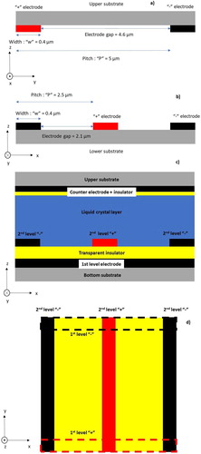
In this work, to verify the electro-optical characteristics of an LC cell using crossed patterned electrodes, one pixel with three variations of the crossed patterned electrodes’ architectures was first simulated. The first structure (structure 1) consisted of two levels of electrodes on the same substrate, separated by a transparent insulator (Figure ).
Figure 2. First pixel structure with two levels of electrodes on the same substrate (‘structure 1’). (a) View of the 2nd-level electrodes for LC addressing. (b) Cross-section along A, 1st-level electrodes for electrical relaxation. (c) Complete view of the pixel structure. (d) Top view of the pixel structure. The 1st-level electrodes below the insulator are in dashed lines.
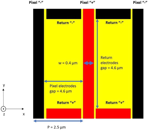
The second structure (‘structure 2’) consisted of one range of electrodes, all on the same level (Figure ).
Figure 3. Second simulated pixel structure with all the electrodes on the same substrate (‘structure 2’).
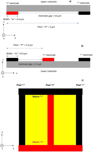
The third structure (structure 3) consisted of one level of electrodes on the bottom substrate for turning on the cell. The turn-off electrodes dedicated to decreasing the fall time were located on the upper electrodes (Figure ).
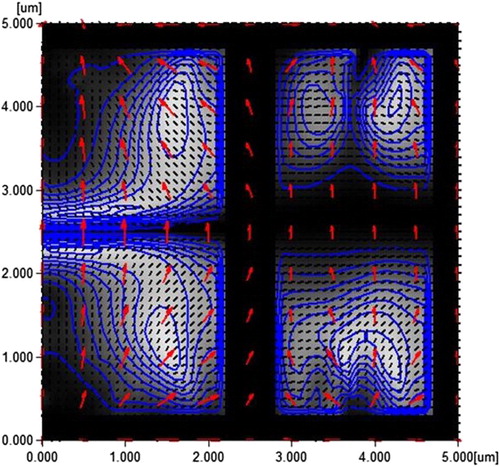
A simulation was done for the three configurations, and two of them were manufactured (structures 1 and 3), assembled, and tested experimentally.
The simulations were performed with the commercially available package LCDMaster 3D (Shintech). In the simulations, 20-µm-thick HLC2-5618 was used as a polarizer. For the experimental characterization, the cell was put under crossed linear polarizers, and a green laser (λ = 532 nm) was used. The data were collected with a photodiode linked to an oscilloscope. All the following characteristics were similar for the three structures. For the electrodes on the top of the insulator set that served as driving electrodes, the width (w) was 0.4 µm, and the gap was 2.1 µm, resulting in a 2.5 µm pitch (P) (Figure (a)). This configuration created two subpixels with a 2.5 µm pitch. The electrodes located underneath were the electrodes that would allow for a fast turn-off. The electrode had a 0.4 µm width and a 4.6 µm gap, resulting in a 5 µm pitch (Figure (b)). They were made of aluminium. The cells were fabricated with the microelectronics processes. Processes like photolithography and etching allow the creation of patterns of electrodes with a very small width (0.4 µm).
Figure 4. Pixel structure of the simulated and fabricated LC cells with the return electrodes on the upper substrate (a) and the driving electrodes on the bottom substrate (b) (structure 3). (c) Top view of structure 3.
To achieve a homogeneous alignment in the LC cell, polyimide (Nissan 7480) was spin-coated on each substrate and baked at 180°C for 15 min. The rubbing direction was set to 3° with respect to the bottom electrodes. Next, the cell was assembled using 2-µm-diameter silica spacers. Finally, the LCs were injected into the cell. The most important parameters of MLC-2062 were k2 = 10.3 pN, Δε = 6.3, Δn = 0.21, and γ1 = 0.22 Pa s, and those of MLC-2139 were k2 = 10.3 pN, Δε = 48, Δn = 0.16, and γ1 = 0.395 Pa s.
3. Simulations results
3.1. Performances of structure 1
In this section, the performed simulation of structure 1 corresponding to Figure is described. The driving electrodes (2nd-level electrodes in Figure (a)) were addressed while the turn-off electrodes (1st-level electrode/buried electrodes in Figure (b)) were kept in a floating state. The voltage transmittance (also called ‘static regime’) curves were ploted to check the cell’s electro-optical characteristics (Figure ).
Figure 5. (a) Voltage-transmittance curve of the simulated cell for MLC-2062. (b) Time-transmittance curve of the simulated cell for MLC-2062.
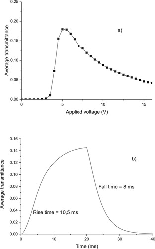
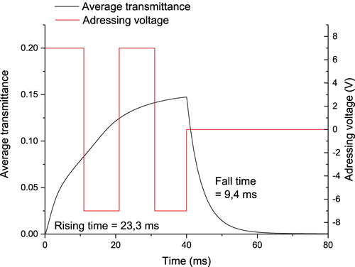
Several square signals, from 0 to 16 V, were simulated and tested at 100 Hz. In Figure (a), a maximum transmittance can be seen at around 0.18 for a 5 V voltage. This behavior indicates a standard behavior of the cell when the driving electrodes are addressed and no interference is observed. This standard behavior is also confirmed in the dynamic mode (time-transmittance curve in Figure (b)). The curve with a square signal at 5 V (100 Hz) for 20 ms was plotted, and the LC went back mechanically to the dark state.
The main objective is to optimize the response time = rise time + fall time. The rise time can be easily reduced by increasing the addressing voltage. The fall time can be reduced by driving the turn-off electrodes. If the buried electrodes are addressed, however, and the 2nd-level electrodes are left in a floating state, no effect on the fall time will be observed. According to the electronic convention, for a normally black configuration, the rise time/turn-on time is defined as the transient time for the transmittance to rise from 10% to 90% of the maximum value, and vice versa for the fall time/turn-off time.
Several voltages were tested at the terminals of the electrodes, from 5 to 20 V (peak-to-peak), by 5 V steps. Figure shows the simulated evolution of the fall time with and without optimization. The state at 0 ms in Figure corresponds to the state at 20 ms in Figure (b).
Figure 6. Evolution of the fall time with and without electrical turn-off.
In Figure , no reduction in the fall time is observed despite the high voltage at the terminals of the buried electrodes (turn-off electrodes). The thickness of the insulator was first suspected to be the cause of this, but the same effect was observed even with a very thin layer of (0.05 µm). Increasing the addressing voltage does not produce any improvement either. To understand this effect, the behavior of the equipotential lines must be looked into again.
Figure shows two distributions of the equipotentials inside the simulated LC cell. The view in Figure is the same as the scheme in Figure (b). In Figure , the red area is the 5 V (a)/20 V (b) area, and the green area is the 0 V area. The color gradient represents the variation of the potential inside the cell. In Figure , several solid lines corresponding to the equipotential lines can be seen. The dashed lines correspond to the orientation of the LC molecules.
Figure 7. Equipotential distribution in the studied LC cell with the buried electrodes at 5 V (red area) (a) and 20 V (red area) (b). The green area is at 0 V.
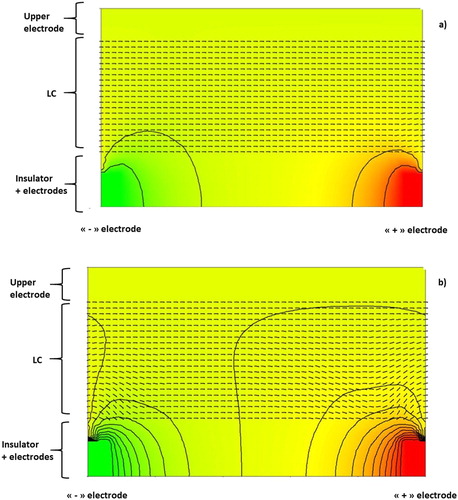
It can be seen in these two figures that the equipotential lines seem to be confined close to the buried electrodes, with almost no effect on the LC molecules. It is also the same for the color variation, because the majority of the green and the red areas are confined close to the electrodes. Only a slight motion of the molecules above the electrodes can be seen in Figure (a), and nothing in the center. All these observations, especially the absence of motion of the LC molecules, are linked to the absence of fall time reduction. To conclude this section, the behavior obtained in Figure was compared with the standard behavior of the equipotential lines for the resulting behavior of Figure (b) at t = 20 ms. This standard behavior is summarized in Figure .
Figure 8. Equipotential distribution in the studied LC cell with the 2nd-level electrodes at 5 V.
The standard behavior of the equipotentials in the LC cell can be observed. If Figure is compared with Figure , a difference in the equipotential repartition will be noticed while looking at the black lines’ behavior. The potential of the electrodes is more spread around the cell, allowing for the LC molecules’ motion.
It was shown that electric turn-off is impossible with two levels of crossed patterned electrodes, due to the containment of the equipotential by the 2nd-level electrodes. In the next section, the origin of this containment will be looked into.
3.2. Origin of the containment of the equipotentials
In this section, the origin of the equipotential containment is investigated. A simulation protocol was established to check the influence of the driving electrodes’ grid.
To investigate the observed effect, it was decided that the first structure introduced in Figure be changed. The LC molecules’ initial orientation and the entrance polarizer angle were set at 3° relative to the return electrodes. By adding two floating electrodes in a floating state in the 2nd level (Figure (a)), the simulation can be made to focus on the influence of these electrodes on the equipotential and transmittance. Figure can be separated into two parts. The first part on the left of the central floating electrode is free from any electrode. The second part corresponds to a subpixel of the final structure (Figure ). The simulation consists of a comparison of the free area and the area with two floating electrodes.
Figure 9. Test structure for the ‘Faraday cage’ investigation.
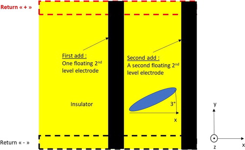
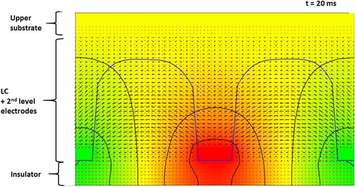
Figure shows the top view of the two-dimensional (2D) spatial repartition of the equipotential lines (black lines) and the electric field (red arrows) of the LC cell with two floating electrodes. Several particular behaviors can be observed. At first gance, the electric field seems to be heading towards the floating electrodes. Then two areas where the equipotential lines are parallel (first and second disclination lines) are indicated. The first disclination line position corresponds to the area where the equipotential lines are parallel and close to one another. The second one on the right also corresponds to an area where the equipotentials are parallel to one another. It is known that the LC molecules, according to their Δε, are aligned perpendicular to the equipotential lines. According to the orientation of the LC molecules and polarizers, disclination lines are created. The influence of all the observed effects on the transmittance was also checked.
Figure 10. Top view of the two-dimensional spatial repartition of the equipotentials, and electric field of the LC cell with two floating electrodes.
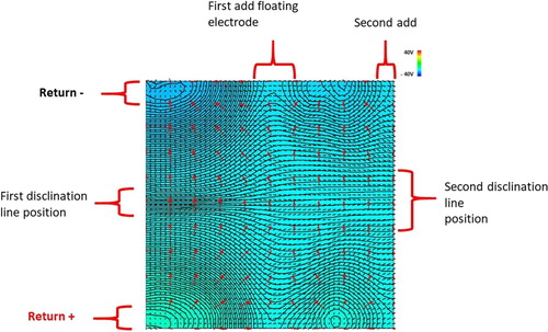
Figure is equivalent to Figure , and the normalized grey-level transmittance was superimposed on the top view of the LC cells. All the blue lines are iso-transmittance lines. The red arrows representing the electric field are shown again, and the LC molecules are represented by black sticks. To come up with an analysable figure and a non-zero transmittance between the two floating electrodes, the ‘return +’ and ‘return −’ electrodes with a square signal at 40 V were addressed. This high-voltage addressing shows a zero-transmittance behavior for the CMOS order voltages.
Figure 11. Top view of the grey-level transmittance, LC molecules’ positions, and electric field for the Figure structure.
The authors’ hypothesis regarding the disclination lines was then verified because there was a zero-transmittance area in the middle of the LC cell, especially between the two floating electrodes, where the disclination line was bigger than the free area.
The explanation of this phenomenon is manifold. Regarding the equipotential lines, when a floating-state electrode is between two addressed electrodes, the equipotentials around the addressed electrodes are deviated and circle the floating electrode. With the configuration herein, it is creating an effect similar to the Faraday cage effect. (The choice of the name ‘Faraday cage’ will be explained later.) Another correlated effect is the behavior of the electric field. It was observed that the electric field coming from the ‘+’ electrode was heading towards a floating electrode. It seems that the floating electrode is behaving like a ‘−’ electrode. According to the floating electrodes theory, when a floating electrode is located between the ‘+’ and ‘−’ voltage electrodes, the potential of the floating electrode stabilizes itself at an average potential [Citation14,Citation15] after a short period of time. This hypothesis was also checked in the simulation, and it was observed that the floating electrode potential stabilizes itself at 0 V when it is located between the +V and −V electrodes.
The behavior shown in Figure can be compared to that shown in Figure . Figure represents the behavior of structure 1 (Figures , , and ). Figure shows the top view of the behavior of the LC molecules with the transmittance inside the cell at t = 0 and 20 ms (Figure (b)). It can be seen that Figure shows the same characteristics as Figure .
Figure 12. Top view of the grey-level transmittance, LC molecules’ positions, and electric field for structure 1 for t = 0 ms (a)/t = 20 ms (b).
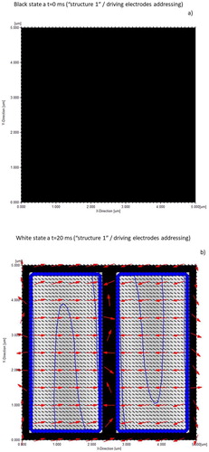
If Figures and are compared, the perfect behavior when the driving electrode was addressed can be confirmed because a perfect dark state preceded it (Figure (a)) and was followed by a perfect white state (Figure (b)). As observed in Figure , in Figure (b), the LC molecules are perfectly oriented, and the electric field (red arrows) is perfectly horizontal. Based on the orientation of the polarizers, a perfect white state can be achieved. This is another proof of the ineffectiveness of the return electrodes for this structure.
In Figure , the transmittance of a complete pixel (Figure ) was plotted according to the LC molecules’ orientation in Figure . This figure confirms the authors’ hypothesis regarding the Faraday cage effect due to the extremely low transmittance (0.05) for a wide voltage range (up to 40 V). A Faraday cage does not allow the outside electric field to go inside the cage, and vice versa. In the case herein, according to Figure , the electrode grid (set in a floating state) above the 1st level allows equipotential deflection. At the same time, the electric field coming from the 1st-level grid is heading towards the 2nd-level grid. It is shown in Figure that the transmittance is close to zero. With all these results, it can be assumed that the 2nd-level electrode grid is blocking the equipotentials and the electric field coming from the 1st-level electrode grid, like a Faraday cage. These behaviors explain the name choice for this effect.
Figure 13. Transmittance of a complete pixel for a high voltage.
According to the initial LC molecules’ orientation, this configuration is ineffective in reducing the fall time because of the Faraday cage effect. To validate this effect, experimental validation was performed.
3.3. Performances of structure 2
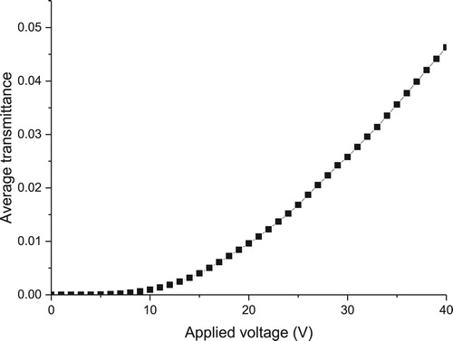
One configuration was eliminated for the fall time reduction investigation. The ‘one-level structure’ (Figure ) was also investigated. As with the previous structure, the rise and fall times were analysed. For the last structure, no improvement was seen due to the Faraday cage effect.
Figure shows the nominal transmittance of the structure shown in Figure . The choice of 7 V was made by analogy to Figure (a), where the maximum transmittance is obtained. The rise time, however, is abnormally long. The reason for this is linked to a disclination line and will be discussed later.
Figure 14. Average transmittance of the ‘one-level structure’ for a 7 V square signal and for the mechanical relaxation of the LC molecules.
In Figure (a), a disclination line is observed and becomes less visible as time increases (Figure (b)). This behavior explains the very long rise time due to the non-homogeneous transmittance. The reason for this inhomogeneity can be the LC molecules’ position. The position of the LC molecules was circled in red, and it was noticed that the authors’ observations were correlated to a previous observation made in Figure .
Figure 15. Spatial repartition of the LC molecules and normalized transmittance at 10 ms (a) and 60 ms (b).
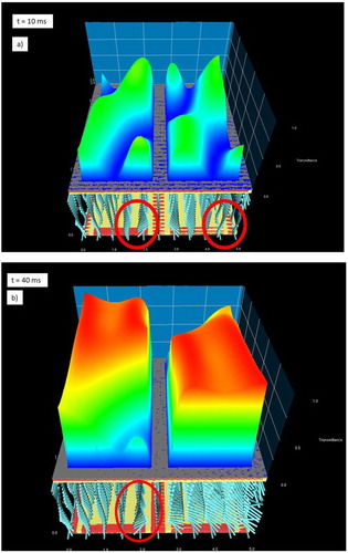
The reason for the disclination lines is linked to the electric field. It can be seen in Figure that the electric field heads towards the floating electrodes because they behave like a fixed potential electrode. If all the electrodes are on the same level, an identical phenomenon is happening, and it creates disclination lines close to the electrodes. According to the LC molecules’ and polarizers’ orientation, they correspond to a zero-transmittance area.
To reduce the rise time, an attempt was made to increase the applied voltage, but the improvements were not significant. On the other hand, it is possible to obtain a reduction in the fall time with this configuration, but in the case herein, contrast problems pose limitations.
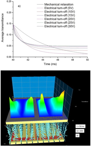
Figure (a) shows a reduction in the fall time when the return electrodes are addressed while the pixel electrodes are in a floating state. It shows a non-zero transmittance, however, for all the voltage values. This phenomenon is identical to that observed in Figure . An interference was obtained between the addressed and floating electrodes. This interference between the electrodes is creating leakage light (Figure (b)) due to the LC molecules’ positions.
Figure 16. Evolution of the fall time with the mechanical relaxation and for different turn-off voltages (a)/spatial repartition of the normalized transmittance and LC molecules 10 ms after the return electrodes’ activation at 30 V (b).
It can be concluded that the structure 2 configuration cannot reduce the fall time because it is impossible to obtain a good dark state with the return electrodes. In the next section, the final structure will be focused on.
4. Simulation and experiment results for structure 3
Structure 3 corresponds to the pixel electrodes on the bottom substrate and the return electrodes on the upper substrate. To evaluate the turn-off with a micropixel, the structure was simulated (Figure ). At the same time, the simulation results will be compared to the experiment results.
The voltage transmittance (also called ‘static regime’) curves were plotted to check the electro-optical characteristics of the LC cell for the two LCs (Figure ).
Figure 17. Voltage-transmittance curve of the experimental cells vs. the simulation cells for MLC-2062 (a) and MLC-2139 (b).
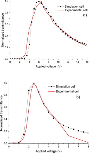
Several square signals, from 0 to 16 V, were simulated and tested at 100 Hz. Several experimental cells were also made. The experiment result is an average of several cells. In Figure (a), a threshold voltage of 3 V and a voltage corresponding to the maximum transmittance (‘nominal voltage’) of 6 V can be observed. When Figure (b) is observed, a lower value for these voltages will be noticed. The threshold voltage is 1 V, and the nominal voltage is 2.5 V. This difference is linked to the Δε of each LC mixture. The threshold voltage is 3 V vs. 1 V, and the nominal voltage, 6.5 V vs. 2.5 V. This result is predictable because the threshold voltage for an IPS configuration [Citation6] is proportional to . According to the electronic convention, for a normally black configuration, the rise time/turn-on time is defined as the transient time for the transmittance to rise from 10% to 90% of the maximum value, and vice versa for the fall time/turn-off time.
To reduce the response time, several voltages were tested. For the rise time, the overshoot method was used. This method is well known [Citation11,Citation12,Citation16,Citation17], and it consists of using the pulse of a voltage higher than the nominal voltage for a short period of time, and then coming back to the nominal voltage. A wide range of voltages have been investigated, from 8 to 20 V RMS (root mean square). The best voltage was 14 V for 0.5 ms for MLC-2062, allowing a rise time of 2 ms, and 6 V for MLC-2139, allowing a rise time of 2.7 ms. For the signal duration, the upper electrodes were in floating potential.
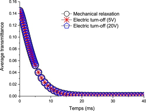
To reduce the fall time, several peak-to-peak (PP) voltages, from 5 to 28 V, were tested for the return electrodes. During these signals, the bottom electrodes were floating (simulation and experiment). The best turn-off times were obtained for 28 V (PP). The average values of 2.15 ms (MLC-2062) and 1.35 ms (MLC-2139) were obtained, the statistic values from several cells.
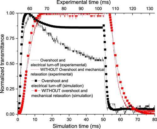
Figure presents the response time evolution with and without a voltage on the upper electrodes with all the best optimizations for MLC-2062.
Figure 18. Experimental switching behavior for the best voltages with and without overshoot/electric turn-off. Applied to MLC-2062.
To validate the simulations herein and to confirm the fastest fall time, the response times were collected for five experimental cells for different voltages, and the experiment results were compared to the simulation results (Figure ).
Figure 19. Average experimental vs. simulation fall times for MLC-2062 (a) and MLC-2139 (b).
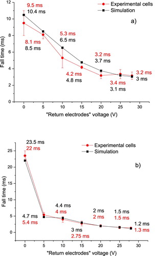
Figure shows the average fall time for several cells and different voltage values, from 0 V (mechanical relaxation) to 28 V. All the signals are still square signals at 100 Hz. The associated error margin was also plotted for both LCs. The same trend was observed in the two figures, with a good fit between the simulation and experiment results.
5. Discussion
Three different structures were simulated, and only one significantly improved the response time (i.e. structure 3). The structure 1 architecture produced the Faraday cage effect. Indeed, in this structure, the driving electrode grid, (the 2nd-level electrodes in Figure (a)) deflected the equipotentials coming from the buried electrodes (the 1st-level electrodes in Figure (a)). Based on these results, it can be assumed that a buried metal plane cannot influence the driving electrode. In this case, a reflective IPS application may be possible because there will be no interference between the buried plan and the driving electrodes.
The ‘one-level structure’ (structure 2) may be of interest for reducing the response time, but further research needs to be done to improve the contrast. With these authors’ investigation, further research could focus on the best architecture: the structure with the return electrodes on the upper substrate. Furthermore, various optimizations can be proposed to further reduce the response time.
The first optimizations in this study were obtained by using the overshoot method to reduce the rise time. The process started from a nominal rise time of 7 ms (MLC-2062) and 10 ms (MLC-2139) to achieve 2 ms (MLC-2062) and 2.7 ms (MLC-2139) response times.
On the other hand, a huge reduction in the fall time was observed, especially for MLC-2139, due to its high |Δε|. There were 9.5 ms (MLC-2062) and 23.5 ms (MLC-2139) mechanical relaxations, and a 28 V (PP) electrical turn-off could reduce the turn-off time to 3.2 ms (MLC-2062) and 1.2 ms (MLC-2139). The higher response time of MLC-2139 can be explained by its higher viscosity (γ1) compared to MLC-2062. With these results, the response times of 4.3 ms (MLC-2062) and 4 ms (MLC-2139) were finally obtained. A reduction of the response time by a factor of four was also obtained for MLC-2062, and by a factor of eight for MLC-2139.
It was theoretically and experimentally confirmed that structure 3 could be used to reduce the response time of a micropixel of a homogeneously aligned positive LC cell. This new micropixel can be an efficient solution for fast-response LC microdisplays. Two specific applications can be reached with this architecture. Due to the high voltage required for electrical turn-off, the first application can be a fast-refreshing display with an external alimentation linked to the ‘return electrodes.’ The second one is an FSC display. If a 180 Hz frequency is assumed, one primary color must be sent to the observer in less than (1/(3*180) s ≈ 1.85 ms). In this work, it was shown that the response time was close to but not exactly at the level required for FSC displays.
When structure 3 was compared with the structures in [Citation9–11] with a turn-off obtained by a vertical field, a full IPS structure with ‘in-plane’ LC molecules (the molecules stay parallel to the substrate) was used. Due to the molecules’ positions, the structure maintained a wide field of view and the IPS’s good constrast. The response time for both LCs with a positive structure 3 was close to the results of [Citation11] (4.3 and 4 ms vs. 3.3 ms). When the turn-off times were compared, 1.2 ms vs. 0.6 ms were obtained for [Citation9] and [Citation10].
Nevertheless, several optimization paths are possible with the use of the proposed architectures. The first optimization can concern the pitch of the upper electrodes (‘return electrodes’). The pitch can be reduced to 2.5 µm. A smaller pixel pitch can reduce the addressing voltage and the response time because the threshold voltage is proportional to the interlectrode gap [Citation6]. Furthermore, MLC-2139 is a very good candidate for the reduction of the response time under 1 ms, especially with this LC mixture, as it is possible to have a fast response time with a low voltage. The rise time can be slightly reduced with the right (voltage/duration) set of overshoot respecting a CMOS maximal voltage. Finally, a non-commercial and home-made LC with control of the most important parameters, such as an LC with a lower viscosity, can be used.
6. Conclusion
In conclusion, all the architectures with return electrodes were reviewed to reduce the response time for in-plane switching (IPS) micropixels. It was shown that only one architecture is possible, and a new effect was highlighted: the ‘Faraday cage’ effect between the buried and surface electrodes. An IPS micropixel with a fast response time was also demonstrated theoretically and experimentally using crossed patterned electrodes. The response time was reduced by the application of the overshoot method to reduce the rise time and the return electrode on the upper substrate associated with high peak-to-peak (PP) voltages for reducing the fall times. Finally, 4 (MLC-2062) and 8 (MLC-2139) reducing factors were obtained with the right set of voltages. With this fast response time, a set of possible applications was also proposed, especially the field sequential color (FSC) application, which becomes reachable with this technology.
Acknowledgement
All the prototypes were manufactured in LETI Clearoom.
Additional information
Notes on contributors

Clément Abélard
Clément Abelard received his Master’s degree in photonics from ENSSAT Lannion in 2015, and his PhD in nano electronics and nano technologies from Grenoble Alps University in 2018. During his PhD studies, his research included IPS technology for phase modulation and fast switching time for microdisplays. He is now working at Holoeye Photonics as a development engineer.

Aurélien Suhm
Aurélien Suhm received his BASc Micro and Nano Technology degree from Grenoble Alps University in 2005, and his M.S. Materials Science degree from CNAM Paris in 2016. His current research interests include OLED and LCD technologies as well as color conversion for microdisplay applications.

Benoit Racine
Benoît Racine is currently working at Emissive Components Laboratory, in the Optronic and Photonic Department, in LETI at Grenoble. In this lab, he is working on LCD and OLED technologies for display and lighting applications. He received his PhD in materials sciences from Picardie Jules Verne University, France in 1999. He joined Emissive Components Laboratory in 2015 to manage LCD-related projects and to support the organization’s OLED activities. He is the author or co-author of around 20 papers about OLED, LCD, amorphous carbon, and diamond-like carbon. He is also the owner or co-owner of 15 patents.

François Templier
François Templier is the research director of CEA-LETI. From 1993 to 1999, he was with Thomson LCD (now Thales Avionics LCD), where he developed new a-Si TFT processes for active-matrix liquid crystal displays. Since 1999, he has been with CEA-LETI, Minatec Campus in Grenoble, France, where his research activity is focused on advanced displays, more particularly emissive microdisplays, flexible displays, and thin-film transistors. He is in charge of strategic marketing for photonics devices at the Optics and Photonics Department. Dr Templier is a member of Society for Information Display, where he is currently the director of the French Chapter.
References
- ED et Network-OSE GmbH, editor. Bildschirme und Anzeigesysteme, ihre Bauelemente und Baugruppen: 17. Electronic displays 2002; Konferenzband (Network-OSE, Hagenburg, 2002).
- W.P. Bleha, L.A. Lei, Advances in Liquid Crystal on Silicon (LCOS) Spatial Light Modulator Technology (2013), p. 87360A.
- F. Templier et al., Development of 5 μm-Pixel Pitch Active-Matrix for Transmissive LCD Picoprojector, présenté à IDW, Japan (2012).
- C.Z. van Doorn, Dynamic Behavior of Twisted Nematic Liquid-Crystal Layers in Switched Fields, J. Appl. Phys. 46 (9), 3738–3745 (1975). doi: 10.1063/1.322177
- M.F. Schiekel, K. Fahrenschon, Deformation of Nematic Liquid Crystals with Vertical Orientation in Electrical Fields, Appl. Phys. Lett. 19 (10), 391–393 (1971). doi: 10.1063/1.1653743
- M. Oh-e, K. Kondo, Electro-Optical Characteristics and Switching Behavior of the In-Plane Switching Mode, Appl. Phys. Lett. 67 (26), 3895–3897 (1995). doi: 10.1063/1.115309
- R. Kiefer, B. Weber, F. Windscheid, G. Baur, 12th Int. Disp. Res. Conf. Jpn. Disp. 5, 547–550 (1992In Plane Switching of Nematic Liquid Crystals).
- G. Baur, R. Kiefer, H. Klausmann, F. Windscheid, In-Plane Switching: A Novel Electro-Optic Effect, Liq. Cryst. Today 5 (3), 12–13 (1995). doi: 10.1080/13583149508047615
- Baek Jong-In, Kim Ki-Han, Kim Jae Chang, Yoon Tae-Hoon, Woo Hwa Sung, Shin Sung Tae, Souk Jun Hyung, Fast In-Plane Switching of a Liquid Crystal Cell Triggered by a Vertical Electric Field, Jpn. J. Appl. Phys. 48 (10), 104505 (2009). doi: 10.1143/JJAP.48.104505
- J.-I. Baek, K.-H. Kim, J.C. Kim, T.-H. Yoon, S.T. Shin, H.S. Woo, P-173: Fast Turn-Off Switching of a Liquid Crystal Cell by Optically Hidden Relaxation, SID Symp. Dig. Tech. Pap. 39 (1), 1846 (2008). doi: 10.1889/1.3069542
- J.-W. Kim, T.-H. Choi, T.-H. Yoon, Fast Switching of Vertically Aligned Negative Liquid Crystals by Optically Hidden Relaxation, Liq. Cryst. 41 (8), 1212–1217 (2014). doi: 10.1080/02678292.2014.911373
- T.-H. Choi, J.-W. Kim, T.-H. Yoon, Fast In-Plane Switching of Negative Liquid Crystals Using Crossed Patterned Electrodes, Jpn. J. Appl. Phys. 53 (8), 081701 (2014). doi: 10.7567/JJAP.53.081701
- M. Oh-e, M. Yoneya, K. Kondo, Switching of Negative and Positive Dielectro-Anisotropic Liquid Crystals by In-Plane Electric Fields, J. Appl. Phys. 82 (2), 528–535 (1997). doi: 10.1063/1.365611
- K.L. Kaiser, Electromagnetic Compatibility Handbook (CRC Press, Boca Raton, 2005).
- P.R.P. Hoole, Electromagnetics Engineering Handbook: Analysis and Structure of Electrical and Electronic Devices and Systems (WIT Press, Southampton; Boston, 2013).
- T.-H. Choi, Y.-J. Park, J.-W. Kim, T.-H. Yoon, Fast Grey-to-Grey Switching of a Homogeneously Aligned Liquid Crystal Device, Liq. Cryst. 42 (4), 492–496 (2015). doi: 10.1080/02678292.2014.1000987
- X.H. Xiduo Hu, Y.S. Yubao Sun, G.Y. Guoqiang Yang, Y.X. Ying Xiang, J.F. Junsheng Feng, Homogeneous-Aligned High-Transmission and Fast-Response Liquid Crystal Display with Three-Layer Electrodes, Chin. Opt. Lett. 10 (1), 011601–011603 (2012). doi: 10.3788/COL201210.011601