
Abstract
Recently, oxide semiconductors-based thin-film transistors have received much attention for biosensor platforms due to their high sensitivity, good chemical resistance, easy surface immobilizations of bioreceptors, and easy fabrication process with solution process or sputtering method. Unlike Si technologies, oxide semiconductors-based thin-film transistors can be fabricated easily and it is highly attractive to make simple sensor arrays. For long-term health-care monitoring, high sensitivity, selectivity, and low-cost chip should be considered. Regarding these issues, metal oxide semiconductors and thin-film transistors are good candidates. Here we address state-of-the-art research trends of biosensors with metal oxide semiconductors-bases thin-film transistors and discuss solution-processing and sputtering methods, separately.
1. Introduction
Oxide semiconductors have been attracting attentions due to their good electrical properties, such as high electron mobility, chemical resistance in liquids, transparency, and easy processing for display and sensor technologies. Although oxide semiconductors-based thin-film transistors (TFTs) have been considered already in the backplanes of liquid crystal displays (LCDs) active matrix organic light-emitting displays these have still been considered other applications, such as biosensors, photosensors, and memory device applications [Citation1–6].
Biosensors have recently developed into intelligent sensors that provide real-time monitoring, early disease detection, and guide new diagnostic directions. They have applied an invasive or non-invasive method for diverse detections of cancer, virus, degenerative brain disorder, diabetes, and depression [Citation7–13]. Biosensors can be assessed by four characteristics selectivity for a specific target, sensitivity to a particular level or trace amount, stable signal detection, and reproducibility in various environments. Recently, the reliability of electronic devices with artificial natural network judgement has been significantly improved and is compatible with clinical analysis (i.e. ELISA) and it can reduce error rates for obtaining high [Citation8,Citation9,Citation14–17]. For the responsive materials of sensors, considering high surface-to-ratio materials are that nanoparticles, nanowires, nanosheets, two-dimensional materials are used widely. It is an essential factor to get high sensitivity of very low concentration of specific targets. In case of electrical platforms, both electrodes and transistors have used widely. The type of transistor gives high sensitivity and can form active matrix device operation. Since ion-selective field-effect transistors (ISFETs) were developed many years ago, the transistors have studied in specific applications using diverse receptors (i.e. aptamer, anitibody, and enzyme) [Citation12,Citation18]. For the channel materials, many candidates have been proposed such as MoS2, IGZO, ITO, In2O3, graphene, PEDOT:PSS and SnO2, and so on [Citation19–26]. In particular, oxide semiconductors have many advantages in universal surface complexation with various molecules, good chemical resistance in electrolytes, and high field-effect mobility (∼50 cm2/Vs), and an ability of easy fabrication.
Here, we focus on state-of-the art technology of oxide semiconductor-based field-effect transistors for biosensor applications beyond display backplane applications. Finally, we will address the prospect of oxide semiconductors as a sensor material that will establish itself as a new application.
2. Sensing techniques and mechanism of TFT-based biosensors
The sensing methods of TFT-based biosensors depend on the type of biotarget. Typically, they are classified into ‘label’ and ‘label-free’-based sensing techniques [Citation27]. The label-based biosensors perform measurements based on fluorescence, electrochemical luminance, and color changes, and recognize the target detection and the concentrations. On the other hand, the label-free methods do not require indicators and give electrical/optical variations. They are also simpler and can easily acquire quantitative and qualitative data, but some devices have different baselines and require the normalization of devices [Citation28]. Applying TFT-based biosensors, the label-free methods are used with the immobilization of the bioreceptors for selectivity.
Depending on the characteristics of the targets, sensors, and environments, the amperometric, impedimetric, conductometric, or potentiometric method can be selected, as shown in Figure (a). The amperometic and potentiometric methods are applied to real-time measurement, and the impedimetric and conductometric methods are used for quantitative analysis and simple target detection [Citation29]. The impedimetric method does not apply to the TFT-based biosensors due to the requirement of a cyclic-voltammetry (C-V) instrument. To realize the selectivity of the target, the coupling of receptors and specific targets, external stimulation transfer, and catalytic reaction are used. There are diverse types of receptors, and antibodies, nucleic acid, enzymes, and cells are applied normally. The antibody–antigen reaction has high selectivity and is used for the detection of viruses and cancer. Blood glucose detection is a representative application with enzyme-based sensors and by-products, where the oxidation/reduction in the targets affects the electrical properties of the sensors. Nucleic acid uses not only the hybridization of deoxyribonucleic acid (DNA) but also the detection of very small concentrated targets with an aptamer (including through the high electron affinity of the DNA, which is applicable for the detection of neurotransmitters, viruses, cancer, glucose, etc.). Living cells are highly sensitive to external stimuli such as stress, toxicity, and organic derivatives, and physiological changes or by-products can be detected by the sensors.
Figure 1. Various receptors-targets coupling and electrical acquisition of sensing data.
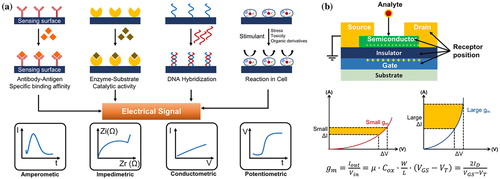
Figure (b) represents the normal TFT structure and the transfer curves of devices for different transconductance (gm) values. The receptors can be immobilized in all the layers, as shown in the TFT structure. When the receptor is immobilized in the gate electrode, dual-gated TFTs are typically used. The potential of the one-sided electrode can be changed when the receptor binds with the target. In the case of the channel layer with a receptor, it is used to detect the target for a very small concentration. The insulator layer has been widely used for ISFETs.
The sensitivity of the sensor strongly depends on the gm. With an increase of the gm value, the current variations are significantly increased for the same potential, rather than with a smaller gm. To increase the gm, thinner, high-mobility, and larger surface-to-volume ratios are considered. In the thinner layer of the channel layer, two-dimensional (2D) materials (graphene, MoS2, and MoSe) have been studied, and quasi-2D In2O3 has also been reported [Citation19,Citation30].
The sensing modulations of the TFT are caused by the electron transfer, the physical changes of the receptors, or the by-products when the receptor binds (or meets) with the target. In the case of pH sensing, the proton concentration is an important parameter of the sensing mechanism. Accordingly, the specific receptors and detection limits must be considered to obtain good sensitivity and selectivity of the targets.
2.1. Solution-processed oxide TFTs for biosensors
With the recent developments in wearable-based health-care sensors and medical devices, the monitoring of various disease factors and health information is attracting much attention, such as non-invasive blood glucose monitoring platforms. Specifically, transistors-based sensing platforms have been proposed widely, and metal oxide semiconductors-based FETs have also received attentions [Citation19,Citation24,Citation26,Citation31,Citation32]. Figure shows a sensor platform that can be used to predict or diagnose degenerative brain disorder regarding Parkinson’s disease. Recently, basic research for the early diagnosis of Parkinson’s disease proposed using oxide TFTs for sensing dopamine, a neurotransmitter [Citation20,Citation21] Dopamine is a small molecule, which makes it difficult to detect very small changes in its concentration. Here, authors used an aptamer as a receptor, which selectively bind to dopamine and the conformational changes of aptamer with dopamine binding affected the charge potential variations on ultra-sensitive In2O3 (∼4 nm thick) surface. It changed the current value of In2O3 FETs, sensitively. The sensors could detect the signal at a Pico molar concentration of dopamine and showed a good selectivity for the different neurotransmitters. In order to form ultra-thin In2O3, water-based indium oxide precursor was used due to their low viscosity and low-temperature annealing capabilities. The solution was found to be capable of decomposition at low temperatures (below 250°C) and exhibited the manifestation of semiconductor properties. Phosphate-buffered saline was used for an electrolyte gating, which was like that of the human body as an environment for detecting dopamine. An electric double layer was formed on the In2O3 surface by closing cations and the device was operated under low voltage driving. The ultra-thin In2O3 has large surface-to-volume ratio and is highly sensitive to change in the surface physical/chemical charge, hence it showed excellent sensing characteristics. It is expected to be used as a detection platform for various biosensors.
Figure 2. Dopamine aptamer immobilized In2O3 biosensors for subnanomolar dopamine detection [Citation20].
![Figure 2. Dopamine aptamer immobilized In2O3 biosensors for subnanomolar dopamine detection [Citation20].](/cms/asset/ac6aab9b-43fc-4bc8-80fc-79d15ce2e490/tjid_a_1714762_f0002_oc.jpg)
Figure shows a sensing approach of a 3.5 nm-thick In2O3 FET-based electrochemical transistors. This work is also done by water-based indium oxide precursors process and form ultra-thin In2O3 FETs. Then the device was decorated with glucose oxidase for a non-invasive glucose detection sensor under tear level [Citation33]. In general, the concentration of glucose in the tears is 3–15 mg/dL (including diabetic concentration aberrations), which is less than one-tenth of the glucose concentration of 70–180 mg/dL in blood [Citation22,Citation33]. Therefore, it is difficult to measure accurate values at low concentrations. In this study, the researchers successfully detected the glucose concentration in tear levels by adsorbing glucose oxidase onto ultra-thin In2O3 FETs and detected the variations of protons as by-products during the oxidation process of glucose. For the selectivity with d-glucose and l-glucose, d-glucose was selectively detected in the range of 100 to 1 µM, while the signal of l-glucose added sensors did not be changed. Authors also fabricated conformal devices on polyimide substrates with a thickness of 1.5 μm and proposed a platform structure that can be attached to surfaces with a wide curvature, such as contact lenses and skin.
Figure 3. Chemical sensing via In2O3 (∼3.5 nm) FET-based conformal biosensors. Pro- and deprotonation of proton variations in different pH onto In2O3. Glucose oxidase gives the selectivity and linearly for different concentrations of glucose [Citation33].
![Figure 3. Chemical sensing via In2O3 (∼3.5 nm) FET-based conformal biosensors. Pro- and deprotonation of proton variations in different pH onto In2O3. Glucose oxidase gives the selectivity and linearly for different concentrations of glucose [Citation33].](/cms/asset/e741a751-2309-4493-9566-8c524af89f19/tjid_a_1714762_f0003_oc.jpg)
A study on the mechanism and reliability of electrolyte-gated transistors using metal oxide semiconductors has also been reported as shown in Figure . Based on solution-processed IGZO TFTs, authors explored the surface behavior of IGZO in electrolyte gating and showed excellent reliability under various salt solutions [Citation34]. In particular, the device worked with the operation voltage of ∼0.5 V under the electrolyte and showed high transconductance of ∼1.0 mS, and on-off ratio of ∼10 [Citation7]. In addition, the bias stress test was performed for 8 h and it was observed that the device could operate without electrical degradation. It is expected that the device can be applied to in vivo system for long-term monitoring environment. The drain current of IGZO-based FETs was increased as an increase of KCL concentrations in water. It could be attributed to an increase in charge accumulation by fully dissolved ions. Figure shows the operation mechanism of IGZO-based electrolyte-gating under physiological environment. It shows that a large number of electrons are accumulated by positive ions closed to the surface of IGZO. This phenomenon formed the electric double layer.
Figure 4. Transfer and output curves (at VG = 0.5 V) of IGZO-EGTFTs employing KCl solutions with various concentrations (from 0 to 2.0 M) [Citation34].
![Figure 4. Transfer and output curves (at VG = 0.5 V) of IGZO-EGTFTs employing KCl solutions with various concentrations (from 0 to 2.0 M) [Citation34].](/cms/asset/a4fb2895-27d7-43be-819a-b8e7b41b87aa/tjid_a_1714762_f0004_oc.jpg)
Figure 5. Electrical properties of IGZO electrolyte-gated thin-film transistors for water and salt solutions as dielectric media [Citation34].
![Figure 5. Electrical properties of IGZO electrolyte-gated thin-film transistors for water and salt solutions as dielectric media [Citation34].](/cms/asset/029a33cf-ec21-49ac-9391-72f0bcbfeefc/tjid_a_1714762_f0005_oc.jpg)
Figure shows the properties of changes of the device in electron trapping and electrostatic interactions by negatively charged phosphate groups on the DNA backbone, occurring when combined with double crossover (DX) DNA nanostructures on the surface of solution-processed IGZO TFTs. It also shows the effect of different DNA concentration on IGZO TFTs [Citation35]. In particular, it is suggested that Cu2+ acts as a current path in the negative gate bias, indicating an increase of the drain current in the depletion region, whereas in the positive gate bias, it acts as a deterring factor of current flow in the back channel region, leading to a decrease in drain current, as shown in Figure . This result indicates that current variations of different DNA concentrations can adopt to a label-free sensor platform using IGZO TFTs.
Figure 6. DNA oxidation and transfer curves of flexible IGZO TFT for the different DNA concentrations [Citation35].
![Figure 6. DNA oxidation and transfer curves of flexible IGZO TFT for the different DNA concentrations [Citation35].](/cms/asset/48738d88-419c-4568-9ca7-3a685dba60e9/tjid_a_1714762_f0006_oc.jpg)
So far, solution-processed metal oxidesemiconductors-based biosensor applications were discussed. The solution-process oxide TFTs have been studied widely to find methods to improve device performance and reduce processing temperatures for display backplane applications but it was difficult for the solution process to compete with the vacuum process. However, discrete biosensors do not require high performance, large area deposition, and flexibility compared with display technologies. Thus, solution-processed oxide TFTs could find a new era of biosensing applications.
2.2. Sputtered-oxide TFTs for biosensors
The research on sputtered-oxide TFT has been studied for a long time, and considerable progress has been made in studies to achieve excellent electrical characteristics and stability for displaying backplane applications. Most recently, sputtered oxide TFTs have also been extended to biosensor applications and their excellent electrical properties are well matched to detect low concentrations of specific target molecules. This section introduces the research trend of biosensor device development using sputtered-oxide TFTs fabricated.
2.2.1. Nanostructured oxide TFTs for biosensors
Figure (a–c) show sputtered In2O3 TFTs-based glucose sensors with the surface modification of source and drain (S/D) electrodes, which was formed by chitosan and carbon nanotube composites [Citation36]. In2O3 films were patterned as nano-ribbon shapes to increase the surface volume-to-ratio. Authors proposed planar structures with all same position of S/D and gate electrodes because solution-gating will not be affected by the position and thickness of liquid dielectric media. The conductance of In2O3 TFTs was changed sensitively to changes in protons caused by decomposition of H2O2 produced by the enzymatic reaction of glucose from the catalytic reaction between glucose oxidase and glucose onto the S/D electrode. The detection ranges showed from 10 nM to 1 mM for the concentrations of glucose, which is acceptable in the glucose levels of sweat and tear.
Figure 7. (a) Device schematics of In2O3 nanoribbon-based TFTs with co-planar Au reference electrodes. (b) The detection properties of the sensors with different human body fluids with artificial tears, sweat, and saliva. (c) Concept images of flexible glucose sensors on the artificial eye and human skin. (d) Dual-gated IGZO TFTs with separated sensing pool for the EBNA-1 antibody detection. (e) The protocol of receptor immobilization. (f) The comparison of detection limit of EBNA-1 antibody for ELISA and IGZO TFTs. (g) Comparison of ELISA and TFT-based sensor platforms [Citation37].
![Figure 7. (a) Device schematics of In2O3 nanoribbon-based TFTs with co-planar Au reference electrodes. (b) The detection properties of the sensors with different human body fluids with artificial tears, sweat, and saliva. (c) Concept images of flexible glucose sensors on the artificial eye and human skin. (d) Dual-gated IGZO TFTs with separated sensing pool for the EBNA-1 antibody detection. (e) The protocol of receptor immobilization. (f) The comparison of detection limit of EBNA-1 antibody for ELISA and IGZO TFTs. (g) Comparison of ELISA and TFT-based sensor platforms [Citation37].](/cms/asset/61ec742a-0a0f-438b-9c37-8ad26206c4aa/tjid_a_1714762_f0007_oc.jpg)
Figure (d–g) propose an isolated sensing pool was separated from IGZO TFTs, which enabled to reuse TFT substrates and it only required the replacement of sensing pools [Citation37]. Authors tried to detect Epstein–Barr virus, selectively, and this virus is known to attack the immune system involving the occurrence malignant tumors such as lymphoma and nasopharyngeal carcinoma. Conventional methods of specific virus detection are related to the antibody–antigen interaction with the activities of the enzymes using the enzyme-linked immunosorbent assay (ELISA) and the results are analyzed by the colorimetric measurement. Figure (f,g) shows the results of comparison between ELISA- and IGZO TFT-based detection limit of Epstein–Barr nuclear antigen (EBNA)-1 antibodies[Citation37]. The detection limit of ELISA was approximately 1 µg/mL, whereas for IGZO TFT, it was 10−4 µg/mL. IGZO TFT-based detection limit was over 10,000 times higher than the ELISA method.
3. Conclusions and outlook
In this review, the state-of-the art technology of biosensor applications with metal oxide semiconductors-based TFTs were addressed in terms of solution-process and sputtering methods. It is very fascinating and promising that metal oxide TFTs-based biosensors that these platforms show highly chemical stability under salt solutions, universal surface complexation with various receptor immobilization, large transconductance for the high sensitivity, and easy fabrication processes. So far, metal oxide TFTs have been considered to apply switching and driving transistors of pixel control in both the backplanes of LCDs and OLEDs, and the device performances have been improved remarkably. Beyond display applications, these progress of metal oxide TFTs are facing sensing applications, such as photo-, bio-, and mechanical sensors.
In particular, core sensor parts of internet of things devices evolving beyond its application in the display field is highly expected to play an important role and provide an opportunity for new advancements in the future.
In addition to the biosensor fields discussed above, it is thought that metal oxide TFTs can also contribute to environmental sensing and automation systems based on new material composition and properties. Currently, when printing-based oxide TFTs have not been drawing much attention in the industry, the transition of its application scope to sensors seems to be adequately positioned. In fact, electronic device manufacturing technology based on printing technologies is not still been regarded in the near future. The broad approach convergence manufacturing technologies, basic materials, and device fabrications related to the integration of silicon and printing process is the result of efforts to create a future staple industry by taking the lead in new technology of oxide TFTs. Thus, new additive printing-based oxide TFT materials, devices, and process technologies are expected to contribute to the creation of new staple industry.
Disclosure statement
No potential conflict of interest was reported by the author.
Additional information
Funding
Notes on contributors

You Seung Rim
You Seung Rim received his B.S. and M.S. degrees from the Department of Electrical and Electronic Engineering of Gachon University, South Korea in 2007 and 2009, respectively, and his Ph.D. from the School of Electrical and Electronic Engineering, Yonsei University, South Korea in 2013. He was a postdoctoral scholar in UCLA from 2013 to 2016 and is currently an assistant professor in the School of Intelligent Mechatronic Engineering at Sejong University in South Korea. His current research interests are wide-bandgap oxide materials and devices, such as oxide TFTs, biosensors, high-power SBDs, and MOSFETs.
References
- E. Fortunato, P. Barquinha, and R. Martins, Adv. Mater. 24, 2945 (2012). doi: 10.1002/adma.201103228
- J. Sheng, H.J. Jeong, K.-L. Han, T. Hong, and J.-S. Park, J. Inf. Disp 18, 159 (2017). doi: 10.1080/15980316.2017.1385544
- S.J. Kim, S. Yoon, and H.J. Kim, Jpn J. Appl. Phys. 53, 02BA02 (2014). doi: 10.7567/JJAP.53.02BA02
- B.D. Ahn, H.J. Jeon, J.Z. Sheng, J. Park, and J.S. Park, Semicond. Sci. Tech. 30, 064001 (2015). doi: 10.1088/0268-1242/30/6/064001
- R.S. Chen, and L.F. Lan, Nanotechnology 30, 312001 (2019). doi: 10.1088/1361-6528/ab1860
- S.P. Park, H.J. Kim, J.H. Lee, and H.J. Kim, J. Inf. Disp. 20, 231. doi: 10.1080/15980316.2019.1664650
- Y.S. Rim, H.J. Chen, B.W. Zhu, S.H. Bae, S.L. Zhu, P.J. Li, I.C. Wang, and Y. Yang, Adv. Mater. Interfaces 4, 1700020 (2017). doi: 10.1002/admi.201700020
- M. Abu Alsheikh, S.W. Lin, D. Niyato, and H.P. Tan, IEEE Commun. Surv. Tutor. 16, 1996 (2014). doi: 10.1109/COMST.2014.2320099
- P. O'Connor, D. Neil, S.C. Liu, T. Delbruck, and M. Pfeiffer, Front Neurosci-Switz 7, 178 (2013).
- C. Chen, Q.J. Xie, D.W. Yang, H.L. Xiao, Y.C. Fu, Y.M. Tan, and S.Z. Yao, RSC Adv. 3, 4473 (2013). doi: 10.1039/c2ra22351a
- Y.S. Rim, S.H. Bae, H.J. Chen, N. De Marco, and Y. Yang, Adv. Mater. 28, 4415 (2016). doi: 10.1002/adma.201505118
- C.I.L. Justino, T.A. Rocha-Santos, and A.C. Duarte, TRAC-Trends Anal. Chem. 29, 1172 (2010). doi: 10.1016/j.trac.2010.07.008
- J.R. Sandifer, and J.J. Voycheck, Mikrochim. Acta 131, 91 (1999). doi: 10.1007/s006040050013
- G.E. Hinton, S. Osindero, and Y.W. Teh, Neural Comput. 18, 1527 (2006). doi: 10.1162/neco.2006.18.7.1527
- J. Torous, M.E. Larsen, C. Depp, T.D. Cosco, I. Barnett, M.K. Nock, and J. Firth, Curr. Psychiat. Rep. 20, 51 (2018). doi: 10.1007/s11920-018-0914-y
- J. Chaki, N. Dey, F.Q. Shi, and R.S. Sherratt, IEEE Sens. J. 19, 3569 (2019). doi: 10.1109/JSEN.2019.2894972
- O. Faust, Y. Hagiwara, T.J. Hong, O.S. Lih, and U.R. Acharya, Comput. Meth. Prog. Biomed. 161, 1 (2018). doi: 10.1016/j.cmpb.2018.04.005
- H.M. So, K. Won, Y.H. Kim, B.K. Kim, B.H. Ryu, P.S. Na, H. Kim, and J.O. Lee, J. Am. Chem. Soc. 127, 11906 (2005). doi: 10.1021/ja053094r
- H.J. Chen, Y.S. Rim, I.C. Wang, C. Li, B.W. Zhu, M. Sun, M.S. Goorsky, X.M. He, and Y. Yang, ACS Nano. 11, 4710 (2017). doi: 10.1021/acsnano.7b00628
- J. Kim, Y.S. Rim, H.J. Chen, H.H. Cao, N. Nakatsuka, H.L. Hinton, C.Z. Zhao, A.M. Andrews, Y. Yang, and P.S. Weiss, ACS Nano. 9, 4572 (2015). doi: 10.1021/acsnano.5b01211
- N. Nakatsuka, K.A. Yang, J.M. Abendroth, K.M. Cheung, X.B. Xu, H.Y. Yang, C.Z. Zhao, B.W. Zhu, Y.S. Rim, Y. Yang, P.S. Weiss, M.N. Stojanovic, and A.M. Andrews, Science 362, 319 (2018). doi: 10.1126/science.aao6750
- M.M. Rahman, A.J.S. Ahammad, J.H. Jin, S.J. Ahn, and J.J. Lee, Sensors-Basel 10, 4855 (2010). doi: 10.3390/s100504855
- J. Rivnay, P. Leleux, M. Ferro, M. Sessolo, A. Williamson, D.A. Koutsouras, D. Khodagholy, M. Ramuz, X. Strakosas, R.M. Owens, C. Benar, J.M. Badier, C. Bernard, and G.G. Malliaras, Sci. Adv. 1 (2015). doi: 10.1126/sciadv.1400251
- D. Sarkar, W. Liu, X.J. Xie, A.C. Anselmo, S. Mitragotri, and K. Banerjee, ACS Nano 8, 3992 (2014). doi: 10.1021/nn5009148
- Y.Y. Shao, J. Wang, H. Wu, J. Liu, I.A. Aksay, and Y.H. Lin, Electroanal. 22, 1027 (2010). doi: 10.1002/elan.200900571
- J.T. Smith, S.S. Shah, M. Goryll, J.R. Stowell, and D.R. Allee, IEEE Sens. J. 14, 937 (2014). doi: 10.1109/JSEN.2013.2295057
- H.K. Hunt, and A.M. Armani, Nanoscale 2, 1544 (2010). doi: 10.1039/c0nr00201a
- S.P. Mohanty, and E. Kougianos, IEEE Potentials 25, 35 (2006). doi: 10.1109/MP.2006.1649009
- D.R. Thévenot, K. Toth, R.A. Durst, and G.S. Wilson, Anal. Lett. 34, 635 (2001). doi: 10.1081/AL-100103209
- W. Wen, Y. Song, X. Yan, C. Zhu, D. Du, S. Wang, A.M. Asiri, and Y. Lin, Mater. Today 21, 164 (2018). doi: 10.1016/j.mattod.2017.09.001
- J. Jung, S.J. Kim, K.W. Lee, D.H. Yoon, Y.G. Kim, H.Y. Kwak, S.R. Dugasani, S.H. Park, and H.J. Kim, Biosens. Bioelectron. 55, 99 (2014). doi: 10.1016/j.bios.2013.11.076
- A. Kahru, H.C. Dubourguier, I. Blinova, A. Ivask, and K. Kasemets, Sensors-Basel 8, 5153 (2008). doi: 10.3390/s8085153
- Y.S. Rim, S.H. Bae, H.J. Chen, J.L. Yang, J. Kim, A.M. Andrews, P.S. Weiss, Y. Yang, and H.R. Tseng, ACS Nano. 9, 12174 (2015). doi: 10.1021/acsnano.5b05325
- S. Park, S. Lee, C.H. Kim, I. Lee, W.J. Lee, S. Kim, B.G. Lee, J.H. Jang, and M.H. Yoon, Sci. Rep. 5 (2015).
- S.J. Kim, J. Jung, K.W. Lee, D.H. Yoon, T.S. Jung, S.R. Dugasani, S.H. Park, and H.J. Kim, ACS Appl. Mater. Interfaces 5, 10715 (2013). doi: 10.1021/am402857w
- Q.Z. Liu, Y.H. Liu, F.Q. Wu, X. Cao, Z. Li, M. Alharbi, A.N. Abbas, M.R. Amer, and C.W. Zhou, ACS Nano. 12, 1170 (2018). doi: 10.1021/acsnano.7b06823
- T.H. Yang, T.Y. Chen, N.T. Wu, Y.T. Chen, and J.J. Huang, IEEE Trans. Electron. Devices 64, 1286 (2017).