
 ?Mathematical formulae have been encoded as MathML and are displayed in this HTML version using MathJax in order to improve their display. Uncheck the box to turn MathJax off. This feature requires Javascript. Click on a formula to zoom.
ABSTRACT
In this study, the effect of a dual microcavity on the luminescent characteristics and light extraction efficiency of organic red light-emitting devices with a multi-cathode structure was investigated. It was clarified that surface plasmon loss on a metal cathode was reduced to about one-fifth and can be efficiently extracted from the outside with the help of the dual-microcavity effect. About half of the radiant energy in dipole emission was successfully utilized as external and substrate modes. The luminous efficiency increased by about 1.52 times, and a narrow-band emission spectrum was observed with a forward directional red emission. The relationship between the luminescence characteristics and the dual-microcavity effect will be discussed from the viewpoint of the optical design of multi-stacked thin film devices.
1. Introduction
Organic light-emitting diodes (OLEDs) are attractive as high-performance flat panel displays in next-generation ultra-high-definition television (TV) sets because of their excellent image quality, high response time, wide viewing angle, and low power consumption. In addition, OLEDs prepared on flexible plastic substrates have the potential to create new markets such as mobile applications as well as light and large public displays. It is well-known that the internal quantum efficiency of OLEDs approaches 100% with the use of the phosphorescence [Citation1] or hyper-fluorescence [Citation2] of excited molecules with proper management of singlet and triplet excitons. However, the external quantum efficiency (EQE) of OLEDs is limited to 20–25% because of the large losses due to their poor light extraction efficiency [Citation3]. Several techniques have been used to improve the light extraction efficiency of OLEDs such as by utilizing an external out-coupling layer, an internal out-coupling layer, a microcavity structure, and a high refractive-index substrate [Citation4]. In the case of display applications, the optical design of the microcavity structure seems effective because the optical interference effect on the multi-staked thin film layers between the high-reflection metal layers makes it possible to enhance the optical intensity in the cavity direction in a specific wavelength range [Citation5]. One problem, however, is the large losses induced by surface plasmon resonance, which is caused by the direct interaction between a metal electrode and the evanescent wave emitted from the vertical dipole moment of the organic molecule. Another problem is that the micro-cavity structure suffers from deterioration of electrical characteristics because the film thickness of the organic layers should be thin as possible for low-voltage operation. However, it is difficult to simultaneously satisfy electrical and optical characteristics because they have a mutual trade-off relationship.
We have already reported that the external microcavity caused by the multi-cathode structure helps improve the emission color and efficiency of the green light-emitting phosphorescent OLED [Citation6]. In this paper, we applied such technology to a red light-emitting device because both the surface plasmon (SP) resonance and the microcavity phenomena are very sensitive to the emission wavelength. From the experiment results and the optical simulation analysis, we will report the relationship between the optical characteristics and the device structure, and the possibility of achieving highly efficient red light-emitting devices with still excellent color purity.
2. Experiment method
2.1. Device structure and preparation
Figure (a) shows a normal device structure, which consists of an indium-tin-oxide (ITO) bottom electrode, a poly(3,4)-ethylendioxy thiophene-polystyrenesulfonate (PEDOT: PSS) hole injection layer, a bis[(1-naphthyl)-N-phenyl]benzidine (NPB) hole-transporting layer, a 4,4’-N,N’-dicarbazole-biphenyl (CBP) emissive layer (EML) doped with a color-emitting guest, a 2-(4-biphenylyl)-5-(4-tert-butylphenyl-1,3,4-oxadiazole) (Bu-PBD) electron transporting layer (ETL), and an aluminum (Al) cathode. A very thin (about 1 nm) lithium fluoride (LiF) film was inserted between Al and ETL to enhance electron injection from the cathode. Each layer was sequentially deposited using the vacuum evaporation technique. The polymer layer of PEDOT:PSS was formed with the spin-coating process. The phosphorescent material of Bis(1-phenylisoquinoline) (acetylacetonate)iridium(III) [Ir(pic)2acac] was used as a color dopant for the red emission. The concentration of the red dopant was fixed at 5 wt.%.
Figure 1. Device structures of the red light-emitting OLEDs with (a) a normal cathode and (b) a multi-cathode.
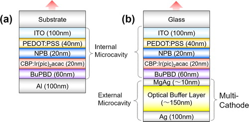
Figure (b) shows the proposed device structure with a dual microcavity, in which the cathode has multiple layers consisting of a semi-transparent MgAg thin film metal, an optical buffer (OB) layer, and a highly reflective silver film. The proposed device structure is called a multi-cathode (MLC) structure. The OB layer uses an ITO film prepared using the rf/dc sputtering method without breaking the vacuum, but other transparent materials such as indium-zinc-oxide (IZO) and low electrical-resistance organic films are available. It should be noted that the MLC structure acts as an optical microcavity outside the device because the transparent OB layer is sandwiched between two kinds of metals. Therefore, we called the MLC structure an ‘external microcavity’ to distinguish it from the microcavity inside the device.
2.2. Optical process and SP analysis
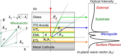
Optical phenomena in an OLED are very complicated because the device consists of a thin film stacked structure of less than one wavelength. The radiation process in the OLED consists of the propagation and evanescent modes. As shown in Figure , the propagation mode is further divided into the external, substrate, and waveguide modes, which are caused by an internal reflection in the thin film layers and the substrate. When the emissive dipole is close to the metal cathode, the evanescent mode such as SP coupling with the metal layer should be further considered to accurately evaluate power dissipation in the device [Citation7]. To calculate the optical modes, it is convenient to introduce the in-plane wavevector kh, which is defined as a horizontal component of the actual wavevector k1. If we use an in-plane wavevector, these optical modes can be arranged one-dimensionally, as shown in the right graph in Figure . The external mode will be treated with classical ray-optics. As for the substrate mode, the wave-optics of incoherent light will be useful. The waveguide mode is strictly calculated with the electromagnetic optics of coherent light. The SP is related to near-field optics. A wide range of wavevectors in optics is deeply involved. The optical calculation was carried out using an original software program that the author developed, which adopted a traditional approach for the dipole model developed for molecular fluorescent and energy transfer near the interface based on near-field optics and wave optics [Citation8].
Figure 2. Relationship between various optical modes and the wavevector inside the organic EL device. The optical modes are divided into the external, substrate, waveguide, and surface plasmon modes. The graph on the right shows a typical optical power intensity dependence for each wavevector.
3. Experiment results and discussion
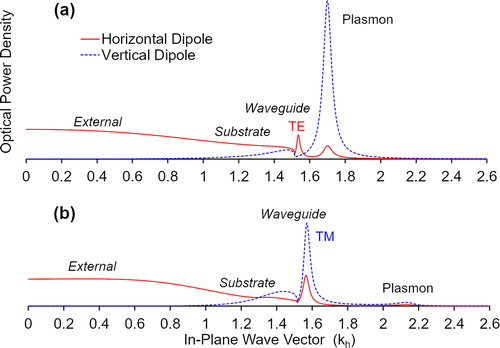
Figures (a) and (b) show the optical power spectra of the OLEDs with the normal and MLC structures, respectively, which indicate the optical energy density in the red light-emission wavelength of 630 nm as a function of the in-plane wavevector kh. Since kh was normalized by the wavevector of air, the horizontal axis corresponds to the refractive index of each material used in the device. The red and blue lines indicate the horizontal and vertical dipoles, respectively. In the normal device, two peaks of the SP loss appeared at 1.70 kh. The SP peak due to the vertical dipole moment was much larger than that due to the horizontal dipole moment, because the SP mainly coupled with the polarized waves present in the vertical dipole moment. In addition, a small sharp peak signed ‘TE’ was observed in the waveguide mode region. The substrate and the external mode due to the horizontal dipole continuously spread over the 0∼1.5 wavevector range. In contrast, when the MLC structure was used, the SP peak almost disappeared and a large waveguide TM mode became dominant in the vertical dipole, as shown in Figure (b). The broad substrate mode also slightly increased.
Figure 3. Optical power spectrum of the dipole emission as a function of the in-plane wavevector. (a) Normal device. (b) Multi-cathode device.
3.1. Internal microcavity
Figure shows a variation of the optical mode ratio with the distance (Ddc) between the dipole and the metal cathode in the device. The dashed and solid lines indicate the normal and MLC devices, respectively. Since it was assumed that the dipole was located at the interface of the light-emitting layer to the electron transport layer (ETL), the distance Ddc was adjusted by the thickness of the ETL. The thicknesses of the semi-transparent MgAg and OB layers were 10 and 150 nm, respectively. The external and substrate modes changed periodically with Ddc. As for the normal device, the external mode took the first maximum of about 60 nm in Ddc. The second maximum appeared near the film thickness of 250 nm. The interval (ΔDdc) between the two peaks in terms of the film thickness was about 190 nm. According to the microcavity theory, the distance (L) between the dipole and the metal cathode that satisfies the microcavity condition is given by the following formula, considering the phase change at the metal electrode, where λ is the optical wavelength.
From this equatio4日n, we see that the interval between the first peak (m = 0) and the second (m = 1) peak as λ/2. In the case of the used device, λ/2 was about 186 nm, assuming that the dominant wavelength of the red emission was 630 nm, and the refractive index of the ETL was 1.69. There is good agreement between ΔDdc and λ/2. This result suggests that the change in the external mode intensity was caused by the internal microcavity effect between the electrodes, including the emission point in the OLED. The optical mode intensity ratios were 20.3%, 22.5%, 3.3%, and 53.9% for the external, substrate, waveguide, and SP modes, respectively. This means that only half of the total energy was available for the propagation light because of a large SP loss, even if the device structure was carefully designed. Therefore, to enhance the light extraction, the SP loss must be suppressed and the waveguide mode must be converted into the substrate and external modes. There are two ways to reduce the SP loss. One way is to suppress the generation of plasmon resonance itself. The other way is to combine the plasmon resonance with the propagating wave and return it to radiation. As shown by the blue solid line in Figure 4, in this study, the intensity of the SP mode in the MLC device decayed exponentially with the increase in Dcd and decreased to less than 10% above 60 nm in Dcd. It should be noted that the waveguide mode increased as the SP loss decreased. The ratios of the external, substrate, and waveguide modes increased to 29.4%, 20.8%, and 39.8%, respectively. Consequently, about 90% of the total radiation energy was available for the propagation light. The mode ratio and its difference in both devices are summarized in Table . The sum of the external and substrate modes increased to about 50% in the MLC device. It is especially worth noting that the waveguide mode increased from 3.3% to 39.8% when the SP loss was recovered to the propagation light. In the future, the increased waveguide mode is expected to be directly coupled with the external microcavity structure.
Figure 4. Variation of the optical energy in the external, substrate, waveguide, and surface plasmon modes with the varied distance between the dipole and the cathode in the devices with normal and multi-cathodes.
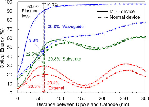
Table 1. Optical power ratio and its difference in the normal and MLC devices
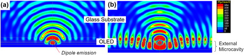
Figure shows color images of the optical power density distributions in the optimized devices with the normal and MLC structures, which were calculated using the finite-difference time-domain (FDTD) method. This calculation was based on the assumption that there was a random dipole emission at the interface of the emitting layer and the ETL. Almost no optical power intensity related to the waveguide mode was observed inside the organic thin film layers of the normal device. The optical power intensity distribution inside the glass substrate spread isotropically. In contrast, the waveguide mode in the film layers was enhanced in the MLC structure. It was especially observed that the propagating wave generated in the external microcavity layers continuously moved to the internal microcavity layers inside the OLED. The results showed that strong light emission occurred in the forward direction.
Figure 5. Color images of the optical power density distribution in the OLEDs, with FDTD analysis used for the optical simulation. (a) Normal structure. (b) Multi-cathode structure.
3.2. External microcavity
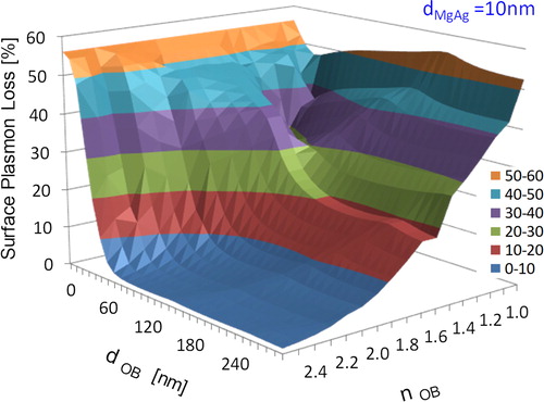
To clarify the role of the MLC structure, we investigated the relationship between the intensity of the SP loss and material parameters, such as the refractive index (nOB) and the film thickness (dOB) of the OB layer, using theoretical simulation. Figure shows a three-dimensional (3D) graph of the ratio of the SP loss as a function of the nOB and the dOB. The thicknesses of the MgAg and Ag layers were kept constant at 10 and 100 nm, respectively. The SP loss intensity rapidly decreased as the dOB increased when the nOB was relatively as high as that of the organic materials used in the device. When the nOB was equal to the refractive index of air (nOB ≒1), the SP loss ratio hardly changed. This means that the reduced SP loss was due to the presence of the OB layer rather than the very thin MgAg electrode. The SP loss ratio decreased to less than 10% in the blue-shaded area characterized by a high refractive index (nOB ≧ ∼1.7) and a thicker film (dOB ≧ ∼50 nm). It is worth noting that as a result, both sides of the extremely thin MgAg layer were symmetric structures sandwiched between dielectrics with similar refractive indices and thicknesses to reduce the SP loss.
Figure 6. Three-dimensional graph of the dependence of the surface plasmon loss intensity on the film thickness (dOB) and the refractive index (nOB) of the optical buffer layer in the MLC device.
Furthermore, we investigated how the SP loss was reduced by increasing the nOB in the MLC structure. Figure shows the changes in the optical power spectrum when the film thickness of the MgAg cathode (dMgAg) was reduced from 100 nm to 10 nm and when the nOB was increased from 1.0 to 1.9. The thickness of the OB layer was kept constant at 150 nm. When the dMgAg was as thick as 100 nm, a strong SP pole appeared at 1.80 in the in-plane k-space. Here, the nOB was set at 1.0 because it was assumed that the OB layer had been replaced by air. This SP pole occurred on the surface of the MgAg layer. The peak position of the SP pole shifted to a higher kh -value with the spread of the half-width as the dMgAg was decreased from 100 nm to 10 nm, as shown in Figure (a) to (d). The SP losses were 49.4%, 48.8%, 43.1%, and 34.3% when the dMgAg was 100, 30, 20, and 10 nm, respectively. Although the peak SP intensity weakened when the dMgAg decreased, the total integration of the SP loss hardly changed because the k-space expanded three-dimensionally with the increase in the wave vector. Next, when the nOB was increased but the dMgAg was kept at 10 nm, the changes shown in Figure (e) to (g) were observed. When the nOB was increased to 1.3, the waveguide mode increased but the broad SP band remained slight. When the nOB was further increased to 1.6, the SP band caused by the MgAg layer completely disappeared. In addition, it is noteworthy that a small amount of the SP pole appeared near 2.0 kh due to the backside Ag reflective layer. This was caused the electric field of the vertical dipole passed through the MgAg layer and reached the Ag layer. In fact, this pole disappeared when the Ag layer was removed. When the nOB was 1.9, which is comparable to that of the ITO film, the waveguide mode further increased. Figure (g) shows the exact optical power spectrum of the MLC device, as already shown in Figure (b).
Figure 7. Changes in the optical power spectrum with respect to the refractive index of the OB layer (nOB) and the film thickness of the MgAg cathode (dMgAg). The dotted line that connects the peaks shows how the surface plasmon (SP) intensity decreased and the waveguide mode increased.
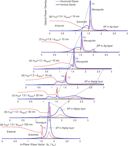
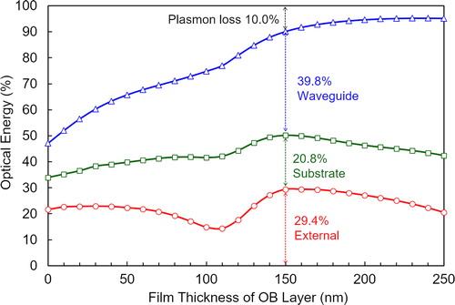
Figure shows a variation of the optical mode distribution when the film thickness (dOB) of the OB layer was 0∼250 nm. When the dOB was zero, it corresponded to the normal device structure with an MgAg/Ag cathode instead of Al. The intensity of the external mode periodically fluctuated and peaked at 29.4% when the dOB was around 150 nm. From this result, it is considered that the maximum efficiency was due to the external microcavity effect, because the thickness of 150 nm is almost equal to 160 nm, which is half of the optical wavelength derived from the red emission wavelength of about 630 nm and the refractive index of the OB layer of 1.97. The small difference can be understood by considering the phase change due to the reflection at the metal interfaces. The SP loss ratio decreased to 10% or less when the dOB was 150 nm or more. The waveguide mode increased instead of decreasing the plasmon loss. These results mean that the evanescent wave was first converted to the propagation mode using the multi-stacked cathode, which was followed by out-coupling with the external mode with the help of the external microcavity effect.
Figure 8. Variation of the optical energy distribution with the variation of the thickness of the OB layer in the MLC device. The optical energy is the sum of the radiations from the horizontal and vertical dipoles.
The detailed optical analysis revealed that the significant reduction of the SP loss was caused by the interaction between two kinds of SP coupling on both sides of the MgAg layer. As the film thickness of the MgAg layer decreased, an evanescent wave of dipole emission penetrated the MgAg layer and reached the OB layer. As a result, long-range and short-range SPs were induced at both interfaces of the MgAg layer [Citation9]. Since the wavevector of the long-range SP was small, it coupled with the waveguide mode, and the short-range SP disappeared because its wavevector exceeded the upper limit of the resonance in the material.
3.3. Device performance
Based on the results of the optical analysis that have been described so far, we fabricated red-emitting OLEDs with a dual-microcavity and investigated their emission characteristics from an optical point of view. Figures (a) and (b) show the dependence of the EQE, luminance, power efficiency, and applied voltage on the current density in three devices with different structures: a reference device with the normal cathode [device (A)], and MLC devices with and without a half-sphere lens [devices (B) and (C), respectively]. The half-sphere lens with the same refractive index as the glass was mounted with index-matching oil on the substrate to measure the total emission intensity of both the external and substrate modes in the device (C). The MLC device (B) exhibited much higher efficiency and luminance than the normal device (A). No significant difference was observed in the voltage versus current density characteristics except for a slight voltage shift in the high-current region, but there was a significant improvement in the emission efficiency. Table compares the EQE and the power efficiency of the three types of devices. The maximum values of the EQE were 20.2% and 30.7% in devices (A) and (B), respectively. That is, the EQE increased by about 1.52 times by adopting the dual-microcavity structure. When the maximum EQE was measured through a half-sphere lens placed on the glass substrate in the MLC device, it increased by up to 48.5% because the optical power in the substrate was extracted out to the air in the external mode. According to the calculation results shown in Table , the sum of the external and substrate modes was 50.2% in the MLC device. The experimental and simulated results were almost the same.
Figure 9. Emission characteristics such as the (a) external quantum efficiency (EQE), luminance, (b) power efficiency, and applied voltage as functions of the current density in the devices with normal and MLC structures. (A) Normal device. (B) MLC device. (C) MLC device with a half sphere lens on the glass.
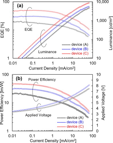
Table 2. Maximum external quantum efficiency (EQE) and power efficiency in the normal and MLC devices.
Figure (a) and (b) show the viewing angle dependence of the electroluminescent spectra in the red light-emitting devices with and without a dual-microcavity, respectively. The normal device exhibited a red emission with a peak wavelength of 634 nm and a broad shoulder band on the long wavelength side. The full width at half maximum (FWHM) of the emission spectra was as wide as 67 nm. The viewing angle dependence of the emission intensity in the normal device was nearly Lambertian, as shown by the semicircle in the figure. In contrast, the FWHM of the emission spectrum narrowed to 51 nm in the MLC device because the shoulder band was significantly suppressed. The strong emission pattern in the forward direction is also attributed to the external microcavity effect. As shown in Table , the color chromaticity (x, y) values of the forward direction are (0.694, 0.303) and (0.690, 0.310) in the normal and MLC devices, respectively. They did not significantly differ because the light emission on the long wavelength side was in the infrared region with low luminous efficiency. However, the chromaticity coordinates of the MLC device changed less significantly than those of the normal device at the viewing angles of 0°, 30°, and 60°.
Figure 10. Viewing angle dependence of the electroluminescent spectrum in the red OLEDs with normal and MLC structures. The semi-circle graphs show the viewing angle dependence of the emission intensity. (a) Normal device. (b) Multi-cathode device.
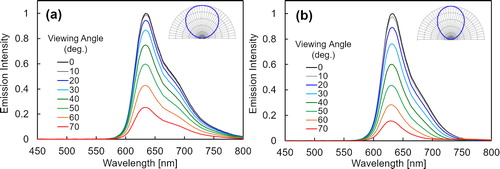
Table 3. Viewing angle dependence of chromaticity coordinates in the CIE 1931 (x, y) diagram for normal and MLC devices.
4. Conclusions
The effect of the dual-microcavity structure on the light emission characteristics was evaluated from the viewpoint of optical calculation and experiments in the red light-emitting OLED. The SP loss was successfully reduced and converted to the waveguide mode in the MLC structure, which enhanced the external microcavity effect. The emission spectrum became slightly sharper and the forward directional emission became strong in the angular distribution. Approximately 50% of the optical power in the dipole emission was converted to the external and substrate modes. The maximum value of the EQE improved to 30.7%, which is about 1.5 times that of the normal device. These optical design methods will be useful for the improvement of the device performance without sacrificing any electrical property.
Acknowledgment
This research activity was supported by the Grant-in-Aid for Scientific Research No. 16K0595700 of the Japan Society for the Promotion of Science.
Disclosure statement
No potential conflict of interest was reported by the author.
Additional information
Notes on contributors

Akiyoshi Mikami
Akiyoshi Mikami received his Doctoral Degree in Electrical Engineering in 1985 from Osaka City University. Subsequently, as a researcher at Sharp Corporation, he worked in Central Research Labs and Liquid Crystal Labs in Sharp Co. for 14 years. In 1999, he was inaugurated as a professor of electronic and optical engineering at the Kanazawa Institute of Technology. His recent research field is the optical design theory and technology for improving the performance of organic light-emitting devices.
References
- M.A. Baldo, S. Lamansky, P.E. Burrow, M.E. Thompson, and S.R. Forrest, Very High-Efficiency Green Organic Light-Emitting Devices Based on Electrophosphorescence, Appl. Phys. Let 75, 4–6 (1999). doi: 10.1063/1.124258
- H. Uoyama, K. Goushi, K. Shizu, H. Nomura, C. Adachi, Highly Efficient Organic Light-emitting Diodes by Delayed Fluorescence, Nature 492, 234–238 (2012). doi: 10.1038/nature11687
- D. Tanaka, H. Sasabe, Y.J. Li, S.J. Su, T. Takeda, and J. Kido, Ultra High Efficiency Green Organic Light-Emitting Devices, Jpn. J. of Appl. Phys 46 (1), L10–L12 (2007). doi: 10.1143/JJAP.46.L10
- W. Brutting*, J. Frischeisen, T.D. Schmidt, B.J. Scholz, and C. Mayr, Device Efficiency of Organic Light-emitting Diodes: Progress by Improved Light Outcoupling, Physica Status Solidi A210 (1), 44–65 (2013). doi: 10.1002/pssa.201228320
- V. Bulovic, V.B. Khalffin, G. Gu, and P.E. Burrowst, Weak Microcavity Effects in Organic Light-emitting Devices, Phys. Rev. B 58 (7), 3730–3740 (1998). doi: 10.1103/PhysRevB.58.3730
- A. Mikami, Highly Efficient and Wide-color-gamut Organic Light-emitting Devices using External Microcavity, J. Info. Disp 20 (3), 135–140 (2019). doi: 10.1080/15980316.2019.1635048
- K.A. Netz, Simulation of Light Emission from Thin-Film Microcavities, J. of Opt. Soc. of America A 15 (4), 962–971 (1998). doi: 10.1364/JOSAA.15.000962
- R.R. Chance, A. Prock, and R. Sibey, Molecular Fluorescence and Energy Transfer Near Interface, Adv. Chem. Phys 37, 3 (1978).
- A. Mikami, Reduction of the Optical Loss in the Multi-Cathode Structure Organic Light Emitting Device Using a Long Range Surface Plasmon, Opt. & Photonics J 6, 226–232 (2016). doi: 10.4236/opj.2016.68B038