
Abstract
The transmittance of the p-doped hole transporting layer (p-HTL) and the charge generation layer (p-CGL) corresponding to the photoluminescence (PL) of blue dopants in an emitting layer decreases as the ratio of the p-dopant increases due to the absorption of the p-dopant. However, there was little difference in the luminous efficiency of blue top-emitting organic light-emitting diodes using p-HTL or p-CGL at a maximum doping ratio of 20%. p-HTL for a single structure required a 5% doping ratio to ensure sufficient electrical characteristics, but p-CGL for the two-stack tandem structure required more than a 10% doping ratio. The optical simulation showed that the device was affected by the specific absorbance of the p-dopant depending on the doping ratio and thickness. Although there was no significant difference in efficiency depending on the doping ratio at a thickness of 10 nm, the reduction rate of the external quantum efficiency increased from over 20 nm due to the doping ratio.
1. Introduction
Organic light-emitting diodes (OLEDs) have been studied along with innovative displays and other developments for the expansion of the display industry [Citation1,Citation2]. The study of organic materials was essential for such intended development. In general, organic materials have a difficult challenge to achieve high conductivity characteristics due to their large band gaps that cause them to have a serious injection height barrier. Therefore, research on charge injection barriers is the most important field that is considered to significantly enhance the efficiency of OLEDs [Citation3,Citation4]. To improve the charge injection, the interlayer between organic materials and electrodes uses such materials as transition metal oxides (RuOx, MoOx, VOx, WOx, etc.) [Citation5–7] and 1,4,5,8,9,11-Hexaazatriphenylene-hexacarbonitrile (HAT-CN) [Citation8], since these interlayers can control the energy level alignment to lower the injection barrier. Recently, however, it has been reported that the electrical doping method more significantly enhances performance than do these materials [Citation9]. Electrical doping adds a small quantity of dopant to the charge transport layer [Citation10,Citation11] to make it easy to fabricate, inexpensive, and capable of alleviating heterogeneity between organic materials. It significantly improves the electrical characteristics such as by decreasing the turn-on voltage or enhancing the conductivity of devices [Citation12]. Moreover, since electrical doping has been studied for a long time, it is the most common and reliable subject of research [Citation13–16].
However, electrical doping easily affects the light-emitting performance of OLEDs because it changes the optical properties of OLEDS, such as their absorption of organic materials [Citation17,Citation18]. Furthermore, no detailed studies have been reported so far on the optical properties of OLEDs to which electrical doping has been applied. Since the main purpose of electrical doping is merely to improve electrical properties, the optical effects of electrical doping have not been considered significant.
In this study, we confirmed that the optical characteristic of a p-dopant varies significantly in the blue wavelength and we reported a difference in the characteristics of OLEDs because of changes in the doping ratio and thickness of the p-doped layers in single and tandem top-emitting OLEDs (TEOLEDs) by optimizing the electrical characteristics of the device.
2. Experiment
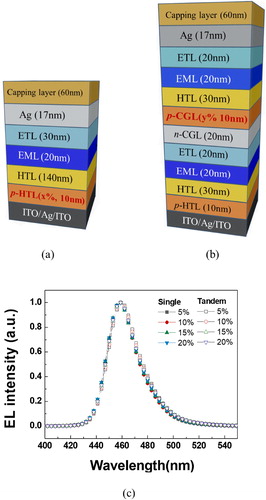
Single and two-tandem blue-fluorescence TEOLEDs were fabricated with identical electroluminescence (EL) units, as shown in Figure . The bottom electrode had been pre-deposited as ITO (5 nm)/Ag (100 nm)/ITO (5 nm) on glass substrates. All the layers in the device had been deposited by thermal evaporation at a high vacuum pressure in the range of 10−7–10−8 torr. In the single blue TEOLEDs, the device included metal layers – a thin-metal transparent top electrode (Ag, 17 nm) – and organic layers – a p-doped hole transport layer (p-HTL, 10 nm) with a varying doping ratio (x%), a hole transport layer (HTL, 140 nm), an emission layer (EML, 20 nm), an electron transport layer (ETL, 30 nm), and a capping layer (CPL, 60 nm). In the tandem blue TEOLEDs, the device included metal layers – a thin-metal transparent top electrode (Ag, 17 nm) – and organic layers – a p-doped (10%) hole transport layer (p-HTL, 10 nm), an HTL (30 nm), an EML (20 nm), an ETL (20 nm), an n-doped charge generation layer (n-CGL, 20 nm), a p-doped charge generation layer (p-CGL, 10 nm) with a varying doping ratio (y%), and a CPL (60 nm). The x and y values of the doping ratio varied (5%, 10%, 15%, and 20%, respectively). Figure (c) shows an optimized EL spectrum of the blue emitter in the single and tandem devices. It means the thicknesses of all the organic layers had been optimized such that the blue-emission wavelength met the micro-cavity condition. [Citation19] Because the deposited organic material was easily degraded, the fabricated device was encapsulated in a nitrogen-filled glove box.
Figure 1. (a) Single blue TEOLED. (b) Tandem blue TEOLED structure. (c) EL spectrum in the single and tandem blue TEOLEDs.
For the optical experiment, the intrinsic and doped layers were deposited on a quartz glass by thermal evaporation for optical measurement, and the transmittance of the intrinsic and doped layers was measured using a UV-Vis-NIR spectrophotometer (LAMBDA 750, PerkinElmer). The refractive index (n) and the extinction coefficient (k) were investigated with a photometric ellipsometer (M-2000, J.A. Woollam). For the electrical studies, the current density–voltage (J-V) characteristics of the devices were measured using a source-measurement unit (Keithley-238, Keithley), and the luminance (L) and electroluminescence (EL) spectra were examined using a spectroradiometer (CS-2000, Konica Minolta). The external quantum efficiency (EQE) in all directions was measured using an integrating sphere equipment (6-inch Halfmoon sphere system, Otsuka Electronics). All the measurement data were taken at room temperature and were measured in a dark atmosphere. Lastly, for the optical simulation studies, the device was used with the OLED optical simulation program SETFOS (Fluxim AG).
3. Results and Discussion
3.1. Optical analysis of the materials
We investigated the optical characteristics of the intrinsic layer and the p-doped layer depending on the doping ratio. Figure (a) shows the transmittance of the intrinsic layer and the p-doped layers in the visible range. As shown in Figure (a), the transmittance characteristics of the intrinsic layer did not vary within the visible light area. In comparison with the intrinsic layer, specific peaks were identified in the blue area (400∼550 nm) from the doping layer. Furthermore, the transmittance linearly decreased as the doping ratio increased. Thus, the p-dopant for electrical doping had properties that influence blue luminescence.
Figure 2. (a) Transmittance and (b) refractive index (n), extinction coefficient (k), and photoluminescence (PL) intensity of the EML.
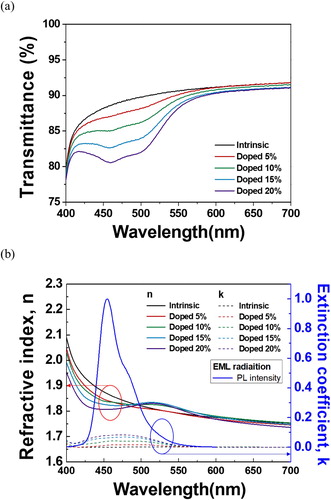
Figure (b) shows the n and k spectra of the intrinsic layer and the p-doped layer, and the photoluminescence (PL) intensity of the EML. The k increased in proportion to the doping ratio in the blue region (400∼500 nm). Furthermore, the PL intensity of the EML radiation overlapped with the k spectra of the p-doped layer. As shown by the decrease in the transmittance according to the doping ratio, the optical effect of electrical doping has the potential to affect the optical performance of a device. n also showed a decrease in transmittance (from 2.1–1.8) in the blue region according to the doping ratio. However, these changes did not significantly affect the optical performance of the device because the variation is usually found in organic materials. [Citation20] Therefore, k is a major factor influenced by the doping ratio.
3.2 Electrical analysis of the device characteristics
Figure (a), (b), and (c) show the current density versus the voltage (J-V), the luminance versus the voltage (L-V), and the current efficiency versus the luminance (ηc-L), respectively, of the single and tandem blue TEOLED devices for different doping ratios in p-HTL and p-CGL. For the single and tandem blue TEOLED devices, all the data were measured by varying the doping ratio (x%) of p-HTL and the doping ratio (y%) of p-CGL.
Figure 3. (a) Current density versus voltage (J-V), (b) luminance versus voltage (L-V), and (c) current efficiency versus luminance (ηc-L) characteristics of the blue TEOLEDs in this study.
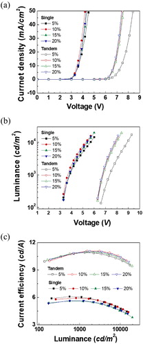
The single blue TEOLED devices that had similar J-V characteristics at all doping ratios are shown in Figure (a). Although their J-V states coincided, they were expected to have a lower turn-on voltage and better performance after electrical doping than the structure with an undoped layer. [Citation21] On the other hand, the tandem blue TEOLED devices showed low performance at the 5% doping ratio and a saturated state at doping ratios above 10%. Since p-CGL interfaces with n-CGL, a relatively low doping concentration of 5% causes large-depletion regions between interfaces. This not only obstructs tunneling injection but also leads to insufficient charge formation [Citation22]. However, the performance of devices at high doping ratios, such as over 10%, is saturated because the fermi energy level is pinned beyond the density of state (DOS) tail of a high occupied molecular orbital (HOMO) even if the doping ratio increases [Citation23].
Figure (b) shows the L-V characteristics of the single and tandem structures. The single structure showed that the devices with 5%, 10%, 15%, and 20% doping ratios had turn-on voltages of 3.9, 3.7, 3.8, and 3.8 V, respectively, at a luminance of 1,000 cd/m2. The device with a doping ratio of over 5% showed a saturation state. The most optimal performance was expected at a doping ratio of over 5% in the single devices. The tandem structure showed that the devices with 5%, 10%, 15%, and 20% doping ratios had turn-on voltages of 7.3, 6.7, 6.7, and 6.8 V, respectively, at a luminance of 1,000 cd/m2. The device with a 5% doping ratio showed low stability and relatively high turn-on voltages, unlike the devices with other doping ratios. This is because, as mentioned above, the formation of charges at a low doping ratio had been insufficient.
Lastly, the ηc-L values of the single and tandem devices at all the doping ratios are shown in Figure (c). The single devices with 5%, 10%, 15%, and 20% doping ratios had current efficiency values of 6.0, 5.9, 5.6, and 5.6 cd/A, respectively, at a luminance of 1,000 cd/m2. As there were slight differences in current efficiency of about 0.4 cd/A at the 5%, 10%, 15%, and 20% doping ratios, the current efficiency of the single devices with over 5% doping ratios was considered saturated, similar to the J-V and L-V characteristics. The tandem devices with 5%, 10%, 15%, and 20% doping ratios had current efficiency values of 10.8, 10.9, 10.9, and 10.9 cd/A, respectively, at a luminance of 1,000 cd/m2. The current efficiency values were similar at all the doping ratios at a low luminance (100∼1,000 cd/m2). However, the device with a low doping ratio of 5% steadily decreased in efficiency at a high luminance (10,000∼20,000 cd/m2), and the device with a 10% doping ratio had the highest efficiency. As mentioned with respect to the J-V and L-V characteristics in the tandem structure, devices with more than 10% doping ratios show saturation in performance, and devices with a low (5%) doping ratio show a drop in performance due to low charge formation.
Since the analysis of the J-V, L-V, and ηc-L characteristics were related only to the forward emission, the integrating sphere equipment was used to evaluate the optical characteristics for all directions for more accurate measurements. Table shows the EQE results obtained with the integrating sphere of the single and tandem blue TEOLEDs at the current densities of 50 mA/cm2 (3,000 cd/m2) and 5 mA/cm2 (1,000 cd/m2), respectively. As shown in the table results, the EQE in the single structures showed similar characteristics regardless of the doping ratio, and the voltage characteristics showed slightly higher voltages (about 0.33 V) at the 5% doping ratio than at the other doping ratios. However, it was difficult to determine the effect of the absorption of the p-dopant in this tendency.
Table 1. Integrating sphere analysis of the single and two-tandem blue TEOLEDs
The tandem structures showed performance differences between the doping ratios of 5% and above 10% at the same current density. The device with a 5% doping ratio showed a low EQE and a high turn-on voltage, unlike the devices with other doping ratios. The tandem devices with a doping ratio of 10% or more had properties that were saturated at an approximately 12.3% EQE and a 6.5 V turn-on voltage. However, this could also be considered the effect of the absorption of the p-dopant. It can instead be interpreted as similar to the electrical variation according to the doping ratio. These results show that the characteristics identified using the equipment were closely related to the resulting electrical characteristics. The insignificant effect of the optical properties of the p-doped layer on the electrical properties is attributed to the very thin (10 nm) p-doped layer. Therefore, these devices with different doping ratios in a thin film (less than 10 nm) did not show a significant effect on the absorption of the p-dopant.
3.3 Optical simulation analysis
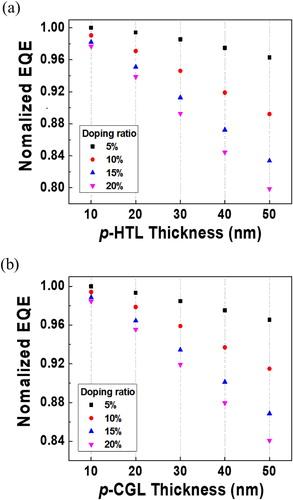
When electrically doped injection layers, such as p-i-n, are the main structure in a device or are significantly thick [Citation24,Citation25], they will affect the optical properties of a device such as its luminous efficiency due to their absorbance of the dopant. Therefore, this study investigated the effect of the dopant by simulating not only the doping ratio but also the factors of the thickness of the electrical doping layer. Figure (a) and (b) show the performance of a device with a normalized EQE according to the doping ratio and the thickness of p-HTL and p-CGL. The thickness of the two layers was varied while the thickness of the HTL was optimized to maintain the cavity length [Citation26]. As shown in the simulation, both the single and tandem structures at the 10nm-thick p-HTL and p-CGL showed only slight EQE differences depending on the doping ratio. The summarized results in Table also show that there were only slight differences in the EQEs of the single and tandem structures depending on the doping concentration of the 10nm-thick p-HTL and p-CGL. The reduction rate due to the doping ratio at 10 nm was insufficient, but the decrease rate due to the doping ratio was noticeable as the thickness increased. It was especially found that the efficiency reduction rate according to the doping ratio increased to up to 16%, as shown in Figure (a), and to up to 13%, as shown in Figure (b), from a thickness of 50 nm. The absorption of the p-dopant was increased by the micro-cavity as the thickness of the top-emitting structure increased. Therefore, both the ratio of the p-dopant with a specific wavelength absorption for electrical doping and the thickness of p-HTL or p-CGL should be considered in designing the structure of the device.
Figure 4. Simulation of the normalized EQE versus the optimized thickness of (a) p-HTL and (b) p-CGL depending on the doping ratio.
4. Conclusion
This study investigated the optical effects of p-HTL and p-CGL on the device. The optical experiment showed a significant optical impact, such as decreasing transmittance through blue absorption of the dopant. However, the electrical experiment showed different optical results. Although the optical properties of the p-dopant were expected to be influenced by the absorption of specific wavelengths, the single and tandem structures did not show varying optical performance according to the doping ratio (maximum: 20%). This suggests that the influence of the p-dopant absorption on the thickness is not significant. However, if the device is designed with a high doping ratio and thickness, the absorption can affect the device. Thus, a device design that considers both the characteristics of the p-dopant and the thickness of the electrically doped layer will improve the performance of the device.
Acknowledgments
This study was supported by the Industrial Strategic Technology Development Program (No. 10079671, Development of a High-Efficiency and Long-Life Blue OLED Material/Device Using a High Horizontal Orientation) funded by MOTIE/KEIT, and by the Basic Science Research program of the National Research Foundation of Korea funded by the Ministry of Education of Korea (2018R1A6A1A03026005).
Disclosure statement
No potential conflict of interest was reported by the author(s).
Additional information
Funding
Notes on contributors

Jaeyoung Park
Jaeyoung Park received his B.S degrees in Creative Convergence Engineering and New Material Engineering from Hanbat National University, Daejeon, South Korea in 2019. He is currently a student in the master’s course at Hanbat National University. He has been working at Reality Device Research Division, ICT Creative Research Laboratory, Electronics and Telecommunications Research Institute (ETRI), Daejeon 34129, Republic of Korea since 2019. His current research interests include electrical doping, optical and electric properties in organic light emitting diodes devices.

Jae-Hyun Lee
Jae-Hyun Lee is an associate professor in the Department of Creative Convergence Engineering at Hanbat National University. He received the B.S. and Ph. D. degree from the Department of Materials Science and Engineering at Korea University in 2002 and Seoul National University in 2011, respectively. Then he worked as a post-doctoral fellow in Institut für Angewandte Photophysik (IAPP) at Technische Universität Dresden (TU Dresden). His research areas include flexible organic electronics and electrically doped organic semiconductors.

Jonghee Lee
Jonghee Lee received his BS, MS, and PhD in Chemistry from the Korea Advanced Institute of Science and Technology (KAIST), Daejeon, Rep. of Korea, in 2002, 2004, and 2007, respectively. He joined Electronics Telecommunications Research Institute (ETRI), Daejeon, Rep. of Korea, in 2007. Then, he moved to the Institut für Angewandte Photophysik (IAPP, Prof. Karl Leo’s group) at the Technische Universität Dresden in Germany as a post-doc in 2010. After 2 years, he joined ETRI again in 2012 and has worked on solution process as well as light-extraction techniques for organic light-emitting diodes (OLEDs). He has been an assistant professor at Hanbat National University, Daejeon, South Korea since 2018.

Hyunsu Cho
Hyunsu Cho Hyunsu Cho received his B.S. and Ph.D. degree in electrical engineering from Korea Advanced Institute of Science and Technology (KAIST), Daejeon, Rep. of Korea, in 2008 and 2014, respectively. He joined Electronics and Telecommunications Research Institute (ETRI) Daejeon, Rep. of Korea, in 2014 and is currently a Senior Researcher. His research interests include the device physics and optical design of optoelectronics devices such as organic light-emitting diodes (OLEDs).
Notes
a J = 50 mA/cm2 (L = 3,000 cd/m2).
b J = 5 mA/cm2 (L = 1,000 cd/m2).
References
- M.A. Baldo, D.F. O’Brien, Y. You, Shoustikov, S., Sibley, M.E., Thompson, and S.R. Forrest, Highly efficient phosphorescent emission from organic electroluminescent devices, Nature 395, 151 (1998).
- Z. Liu, M.G. Helander, Z. Wang, and Z. Lu, Band alignment at anode/organic interfaces for highly efficient simplified blue-emitting organic light-emitting diodes, J. Phys. Chem 114 (39), 16746–16749 (2010).
- R.J. Murdey, and W.R. Salaneck, Charge Injection Barrier Heights Across Multilayer Organic Thin Films, Jpn J Appl Phys 44 (6R), 3751 (2005).
- Z.B. Wang, M.G. Helander, M.T. Greiner, J. Qiu, and Z.H. Lu, Analysis of charge-injection characteristics at electrode-organic interfaces: Case study of transition-metal oxides, Phys. Rev. B 80 (23), 235325 (2009).
- S. Tokito, K. Noda, and Y. Taga, Metal oxides as a hole-injecting layer for an organic electroluminescent device, J. Phys. D: Appl. Phys 29, 2750 (1996).
- C.W. Chu, S.-H. Li, C.-W. Chen, V. Shrotriya, and Y. Yang, High-performance organic thin-film transistors with metal oxide/metal bilayer electrode, Appl. Phys. Lett 87, 193508 (2005).
- C. Adachi, K. Nagai, and N. Tamoto, Molecular design of hole transport materials for obtaining high durability in organic electroluminescent diodes, Appl. Phys. Lett 66 (20), 2679–2681 (1995).
- Y. Dai, H. Zhang, Z. Zhang, Y. Liu, J. Chen, and D. Ma, Highly efficient and stable tandem organic light-emitting devices based on HAT-CN/HAT-CN: TAPC/TAPC as a charge generation layer, J Mater Chem C 3 (26), 6809–6814 (2015).
- H. Cho, C.W. Byun, C.M. Kang, J.W. Shin, B.H. Kwon, S. Choi, and M. Kim, White organic light-emitting diode (OLED) microdisplay with a tandem structure,, J. Inf. Disp 20 (4), 249–255 (2019).
- J. Huang, M. Pfeiffer, J. Blochwitz, A. Werner, J. Salbeck, S. Liu, and K. Leo, Low operating voltage and high efficiency organic multilayer electroluminescent devices with p-type doped hole injection layer, Jpn J Appl Phys 50 (11R), 110202 (2011).
- W. Gao, and A. Kahn, Effect of electrical doping on molecular level alignment at organic–organic heterojunctions, Appl. Phys. Lett 82 (26), 4815–4817 (2003).
- M. Pfeiffer, K. Leo, X. Zhou, J.S. Huang, M. Hofmann, A. Werner, and J. Blochwitz-Nimoth, Doped organic semiconductors: Physics and application in light emitting diodes, Org. Electron 4 (2-3), 89–103 (2003).
- H. Aziz, and Z.D. Popovic, Study of organic light emitting devices with a 5, 6, 11, 12-tetraphenylnaphthacene (rubrene)-doped hole transport layer, Appl. Phys. Lett. 80 (12), 2180–2182 (2002).
- J. Blochwitz, M. Pfeiffer, T. Fritz, and K. Leo, Low voltage organic light emitting diodes featuring doped phthalocyanine as hole transport material, Appl. Phys. Lett 73, 729 (1998).
- J.H. Lee, and J.J. Kim, Interfacial doping for efficient charge injection in organic semiconductors, Phys. Status Solidi A 209 (8), 1399–1413 (2012).
- X. Zhou, M. Pfeiffer, J.S. Huang, J. Blochwitz-Nimoth, D.S. Qin, A. Werner, and K. Leo, Low-voltage inverted transparent vacuum deposited organic light-emitting diodes using electrical doping, Appl. Phys. Lett 81 (5), 922–924 (2002).
- M. Petrosino, P. Vacca, R. Miscioscia, G. Nenna, C. Minarini, and A. Rubino, Effect of PEDOT: PSS ratio on the electrical and optical properties of OLEDs, Photonic Materials, Devices, and Applications II. Vol. 6593. International Society for Optics and Photonics (2007).
- M.L. Tietze, J. Benduhn, P. Pahner, B. Nell, M. Schwarze, H. Kleemann, and K. Leo, Elementary steps in electrical doping of organic semiconductors, Nat. commun 9 (1), 1–9 (2018).
- S. Hofmann, M. Thomschke, B. Lüssem, and K. Leo, Top-emitting organic light-emitting diodes, Opt. Express 19 (106), A1250–A1264 (2011).
- H. Shin, J.H. Lee, C.K. Moon, J.S. Huh, B. Sim, and J.J. Kim, Sky-blue phosphorescent OLEDs with 34.1% external quantum efficiency using a low refractive index electron transporting layer, Adv. Materials. 28 (24), 4920–4925 (2016).
- J.H. Lee, D.S. Leem, and J.J. Kim, High performance top-emitting organic light-emitting diodes with copper iodide-doped hole injection layer, Org. Electron 9 (5), 805–808 (2008).
- H. Sun, Q. Guo, D. Yang, Y. Chen, J. Chen, and D. Ma, High Efficiency Tandem Organic Light Emitting Diode Using an Organic Heterojunction as the Charge Generation Layer: An Investigation into the Charge Generation Model and Device Performance, Acs Photonics 2 (2), 271–279 (2015).
- S. Olthof, W. Tress, R. Meerheim, B. Lüssem, and K. Leo, Photoelectron spectroscopy study of systematically varied doping concentrations in an organic semiconductor layer using a molecular p-dopant, J Appl Phys 106 (10), 103711 (2009).
- R. Meerheim, B. Lussem, and K. Leo, Efficiency and stability of pin type organic light emitting diodes for display and lighting applications, P IEEE. 97 (9), 1606–1626 (2009).
- J.F. Li, S.F. Chen, S.H. Su, K.S. Hwang, and M. Yokoyama, Effects of hole injection layer thickness on the luminescent properties of white organic light-emitting diodes, Appl Surf Sci 253 (5), 2522–2524 (2006).
- E. Jung, H. Lee, H. Chae, and S.M. Cho, Effect of hole-transport-layer thickness on deep-blue emission in top-emitting cavity organic light-emitting diodes, Electron Mater Lett 11 (5), 764–768 (2015).