
 ?Mathematical formulae have been encoded as MathML and are displayed in this HTML version using MathJax in order to improve their display. Uncheck the box to turn MathJax off. This feature requires Javascript. Click on a formula to zoom.
Abstract
Top-emission organic light-emitting diodes (TEOLEDs) that contain semi-transparent metal top cathodes and highly reflective anodes have been actively researched for display applications due to their many advantages such as their high aperture ratio, good color purity, and high efficiency. In this research, the technical design of TEOLEDs used in organic light-emitting diode (OLED) displays is reviewed, covering the optical theory with the microcavity effect, optical losses, and the importance of the Purcell effect in the optical calculation. The key methodologies for addressing the high efficiency and low driving voltage of TEOLEDs are also discussed.
KEYWORDS:
1. Introduction
Since Tang and Vanslyke [Citation1] discovered the first organic electroluminescence (EL) in 1965 [Citation2], many developments in organic light-emitting diodes (OLEDs) have been introduced. The many OLED advantages such as their light weight, fast response time, high aperture ratio, low driving voltage, vivid colors, and surface emission make them good materials for display applications. In 2000, Sanyo and Kodak released a prototype of a 5.5-inch OLED TV with active matrix (AM) driving. With the continued development of display technology, OLED has been applied not only to TVs but also to mobile phones. Today, LG and Samsung mainly produce OLED panels for TVs and mobile phones, respectively.
The OLED multilayer structure generally contains electrodes, carrier transport layers, and the emissive layer (EML). The injected hole and electrons from the anode and cathode are recombined in the EML through the hole transport layer (HTL) and the electron transport layer (ETL). The OLED structure can be classified according to the output direction of the generated light. Thus, there are bottom-emitting (BE) OLEDs and top-emitting (TE) OLEDs. Therefore, BEOLEDs and TEOLEDs have different structures and different optical phenomena [Citation3,Citation4]. The display generally contains electrodes, capacitors, and thin-film transistors (TFTs) that drive the OLED device. The initial OLED display used a passive matrix (PM) driving method, which is driven line by line [Citation5,Citation6]. On the other hand, the active-matrix OLED (AMOLED) needs to drive pixel by pixel to control the high-resolution image. Thus, the AM driving method has driving and switching TFTs with capacitors [Citation7–9]. These TFTs are fabricated on the substrate before the fabrication of the OLED pixel. In the case of BEOLEDs, there is a limitation in the resolution of small devices due to the existence of TFTs and capacitors in the light-emitting direction. On the other hand, there is no decrease in the aperture ratio in TEOLED-based AMOLEDs.
Until now, various technologies still being developed for TEOLEDs. Because of the thinness of the entire structure of TEOLEDs, they have various optical interferences. To predict such interferences, optical calculations are important. The Fabry–Perot resonator model is initially used to model TEOLEDs because its structure is similar to that of TEOLEDs [Citation10,Citation11]. Then dipole emission in planar structures is considered using an electromagnetic model [Citation12,Citation13]. Using these developed models, various simulators are developed such as SimOLED [Citation14,Citation15], SETFOS [Citation16,Citation17], FEM [Citation18,Citation19], and FDTD [Citation20,Citation21]. Besides these optical calculations, common layers such as HTL, ETL, EML, electrodes, and the capping layer (CPL) have been developed for TEOLED. The p and n doping methods are also used to enhance the mobility of the carrier transport layers [Citation22–25] and to improve their refractive index so as to enhance the efficiency of the TEOLED [Citation26]. As for EML, various dopants with a high quantum yield and a long lifetime have been developed. The narrow bandwidth dopant is especially being studied to enhance color purity and because of its applicability to TEOLEDs [Citation27]. The metal electrode structure is likewise being developed to enhance the TEOLED efficiency. Magnesium (Mg) doped with a silver (Ag) cathode (Mg:Ag) at a 1:10 ratio is currently being used to mass-produce cathodes for TEOLEDs. Besides these cathodes, pure Ag, Ag-doped other metals, and the multilayer structure are being studied [Citation28,Citation29]. In addition, CPL is being studied to improve the TEOLED efficiency while controlling its refractive index and optical structure.
In this research, we discuss optical design methods such as the optical theory, power dissipation calculation, and the Purcell effect to more accurately analyze the technical design of TEOLEDs. We also discuss the material technologies needed to achieve high-efficiency TEOLEDs, such as HTL, EML, ETL, semi-transparent metal cathodes, and CPL.
2. Optical calculation technologies
2.1. Optical theory
The bottom-emission light-emitting diode (BEOLED) is the structure that was used in the initial AMOLED display. It had a transparent anode and a reflective cathode, and emitted light from the anode direction. To reflect all the light towards the anode direction, a thick metal cathode such as aluminum (Al) was used. For the anode, high-transmittance indium tin oxide (ITO) was typically used to emit as much light as possible [Citation30,Citation31]. There was a strong and weak reflection in the cathode and the anode, respectively. Due to the reflective electrodes, there was optical interference between the emitting light and the reflective light from the electrode (two-beam interference) [Citation32,Citation33]. This internal optical phenomenon is important because the change in the internal condition produces different output spectral intensities. This interference also appears in TEOLED, which is composed of a reflective anode and a semi-transparent metal cathode. For the reflective anode, an ITO/Ag/ITO multilayer structure is used due to its high reflectivity (over 90%) [Citation34]. For the cathode material, a transparent conductive oxide material (ITO) is difficult to apply because of the damage issue due to the sputtering process [Citation35]. Thus, a thin metal film such as the Mg:Ag alloy and Ag are used for the semi-transparent cathode due to their high transmittance and high conductivity [Citation36,Citation37]. Because of both reflective electrodes in TEOLED, there are multiple reflections, and they cause more complex interferences than those in BEOLEDs. In addition to two-beam interference, there is a multi-resonance interference between both electrodes. Because the structure of TEOLEDs is similar to that of the Fabry-Perot resonator, which contains parallel mirrors (similar to reflective electrodes) [Citation38–40], this effect is strong in TEOLED due to the reflectivity of both electrodes. This two-beam interference and the Fabry-Perot interferences are the main factors in determining the output spectral intensity of TEOLED. This optical effect is called the ‘micro-cavity effect.’ To match the constructive interference condition, different device thicknesses are applied according to the resonance wavelength. The thickness conditions are especially changed according to the emitting resonance wavelengths of the blue (460 nm), green (530 nm), and red (610 nm) colors. Because the structure of the device is complex and thick, it must be designed before the TEOLED is fabricated. To predict the output spectral intensity of the TEOLED, this device can be expressed as a Fabry-Perot resonator [Citation41,Citation42]. Using this structure and the two-beam interference condition, the output spectral intensity can be calculated as follows [Citation43]:
(1)
(1) wherein
is the internal spectral intensity,
is the wavelength of the emitting light, R is the reflectivity of the electrode (R1: anode and R2: cathode),
is the phase shift of the electrode,
is the emission angle, z is the distance between the anode and the EML, and L is the distance between the two electrodes. Figure (a) shows a schematic of Equation (1). The output spectral shape and the radiance value can be determined by using Equation (1) for the cavity structure. Especially, because R1 has an almost fixed value of about 90% or more, the output spectrum is mainly determined by R2, the transmittance of the cathode (1 − R2), and the cavity length, which has a proper interference condition in TEOLED. Excluding the properties related to electrodes, L and z are important values in designing TEOLEDs. To create a constructive interference using a two-beam interference, the thickness of z must be controlled. If z is fixed, the output spectral intensity is determined by L. To match the resonance wavelength with the constructive interference condition, L must be controlled. By controlling z and L, TEOLED can satisfy the constructive interference condition for each color, as shown in Figure . The thinnest device with a low constructive interference condition is the 1st order cavity. As the thickness increases, the 2nd and 3rd order conditions can be designed. Thus, the electrode properties and the organic layer thickness are important in the optical design of TEOLEDs. The spectral width also varies with the micro-cavity effect. The full width at half maximum (FWHM) shows the strength of the micro-cavity effect and can be calculated as follows [Citation44]:
(2)
(2) wherein
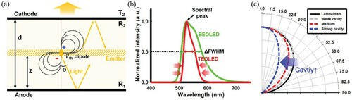
is the cavity length between the two electrodes. The equation shows that TEOLEDs with a long cavity and highly reflective electrodes have a low FWHM value when the output spectral width is narrowed [Citation45]. Figure (b) shows the emission spectra of Ir(ppy)3 with and without the micro-cavity effect. The reduced FWHM shows high color purity due to the enhanced single wavelength, but it can cause a bad viewing angle property due to the variation of the Lambertian emission pattern [Citation46,Citation47]. Figure (c) shows the emission pattern of OLEDs. The BEOLED showed a Lambertian-like emission pattern, which is caused by the weak micro-cavity effect. If the anode is replaced with a reflective material in the BEOLED, an emission pattern narrower than the Lambertian pattern can be achieved due to the micro-cavity effect. Similarly, TEOLEDs can show a Lambertian emission pattern if the cathode material has high transmittance. The measured color coordinates from 0 to 60 degrees with different cavity conditions are given in the reference paper [Citation48]. The TEOLED showed a color coordinate variation of (−0.03, −0.03) due to the strong micro-cavity condition. However, the BEOLED showed no variation in the color coordinates (with an emission pattern almost similar to the Lambertian pattern). This means the cavity effect affects the emission pattern and the viewing angle property in TEOLEDs.
Figure 1. Structures of red, green, and blue TEOLEDs with R′, G′, and B′ layers, respectively [Citation94].
![Figure 1. Structures of red, green, and blue TEOLEDs with R′, G′, and B′ layers, respectively [Citation94].](/cms/asset/d9dcba6c-7981-45c3-8c74-d5bb29ee4679/tjid_a_1876173_f0001_oc.jpg)
Figure 2. (a) Schematic of TEOLEDs, (b) spectral shape of Ir(ppy)3 according to the presence of the micro-cavity effect, and (c) emission with the angle distribution and the intensity of the cavity effect.
Besides this optical effect, the device characteristics can be affected by various emitting materials, the order of the cavity condition, the optimization of the cathode, and the CPL. These characteristics will be discussed in Sections 2.2 and 2.3.
2.2. Optical loss calculation method for TEOLEDs
For more sophisticated calculations for TEOLEDs, the power generated from the spontaneous emission of the dipole must be considered because the previous calculation method only checks the output spectral characteristics and does not accurately consider the optical loss mechanism. To analyze optical characteristics such as the influence of the metal type and different organic materials, additional calculation is needed. Also, the cause of characteristic variations in TEOLEDs must be analyzed. First, the total power of the TEOLED in an infinite medium can be calculated by assuming a forced damped harmonic oscillator model [Citation49,Citation50]. The total dissipated power must satisfy the following equation [Citation49,Citation50]:
(3)
(3) wherein u is the in-plane wavevector component,
is the internal quantum efficiency of the emitting dipoles, and K(u) is the power dissipation density per unit wavevector u. The internal quantum efficiency can be determined as follows [Citation51]:
(4)
(4) wherein
and
are the radiative and non-radiative decay rates, respectively, of the emitting dipole [Citation51]. K(u) can be calculated at randomly oriented dipole emitters. The transverse magnetic (TM) and transverse electric (TE) wave modes must be especially considered. The dipole coupling of the TM and TE modes can be calculated for a randomly oriented dipole as follows [Citation52,Citation53]:
(5)
(5)
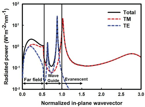
These three components include horizontal and vertical dipole coupling of the TM and TE modes in the total power density [Citation52,Citation53]. Especially, this different wave mode produces different optical phenomena. Afterwards, the total radiated power is classified into different contributions such as the air/substrate guide mode, absorption loss, the surface plasmon, and far-field radiation. Furno et al. reported a detailed power density calculation method [Citation53]. Figure shows the calculated power dissipation spectrum of a TEOLED device. The structure of the calculated TEOLED is shown in the reference paper [Citation54]. It is divided into several regions such as for the far-field out-coupling, the waveguided mode, and the evanescent mode with a surface plasmon depending on the normalized u. In these spectra, the TM and the TE modes show different tendencies. The TM mode has a higher far-field radiated power than the TE mode. However, a large amount of the TM mode corresponds to the evanescent region because the TM mode mainly causes surface plasmon loss in TEOLEDs. However, the TE mode has strong radiative power in the waveguided mode. Thus, the TM and TE modes can affect different loss mechanisms in TEOLEDs, so they must be controlled to achieve optically high efficiency [Citation55–57].
Figure 3. Calculated power dissipation spectra of TEOLEDs.
2.3. Advance calculation with consideration of the Purcell factor
To accurately design TEOLEDs, various calculation methods have been used [Citation3,Citation58–60], including the previously discussed calculation method, and are continuously being improved. The output efficiency of the multi-layered structure can be calculated using the transfer matrix method and the Fresnel equation. However, the previously discussed calculation of TEOLED does not consider the Purcell effect. This effect occurs when the emitter makes a spontaneous emission near the electrode. Then Fermi’s golden rule [Citation61,Citation62] affects the variation of the radiative decay rate of the emitter. TEOLEDs can be especially easily affected because of their complex interference condition and because both their electrodes are metal. Thus, the cavity mode device must consider this effect. This calculation method was established by Neyts et al. in 1996 and has been used in many researches [Citation63]. The general equation for the external quantum efficiency (EQE) is:
(6)
(6) wherein quantum static is the singlet and triplet ratio in the emitter,
is the electrical recombination efficiency of the electrons and holes, and
is the out-coupling efficiency. In the micro-cavity mode, the radiative decay rate
is changed to
which is the effective radiative decay rate due to the cavity effect.
is represented as
and
is related to the total power dissipation in the device structure and is called the Purcell factor. This factor can express the influence of the Purcell effect in the TEOLED calculation. Similarly,
is changed to the effective
and can be represented by the following equation [Citation60]:
(7)
(7)
Following this, the quantum static and can be defined as constants and the EQE equation for the micro-cavity condition can be summarized as
(8)
(8) wherein
is replaced with n for convenient calculation. For commonly used materials, n is converged with 0 due to the relation
. As a result, the EQE value is proportional to
. Thus, the Purcell factor must be considered in the optical simulation. Cho et al. reported their use of the OLED optimization method by applying the Purcell factor in the calculation [Citation64]. They performed an optical simulation of BEOLED and TEOLED using two methods, depending on the Purcell factor. The simulation results showed a large difference between TEOLED and BEOLED, which indicates that in a simulation with the Purcell factor, the calculation results are closer to the experiment results. The calculation results are shown in Figure and Table . The structure used in the calculation is shown in reference [Citation53]. Based on the efficiency of the 1st-order TEOLED, the 2nd- and 3rd-order TEOLEDs are compared with various emitter positions. The calculation results especially differ according to the Purcell factor in the 2nd-order TEOLED. The efficiency of the 3rd-order TEOLEDs also significantly increased after the Purcell factor was applied. As a result, the efficiencies of the two-stacked (2nd-order) and three-stacked (3rd-order) tandem devices changed. In the calculation without considering the Purcell factor, the three-stacked structure showed 1.76 times higher efficiency than the 1st-order TEOLED. After the Purcell factor was considered, the enhancement ratio increased 4.06 times. It means that the Purcell factor is significantly affected by the position of the emitter near the metal electrode, and that considering the Purcell factor enables more accurate calculation of these devices.
Figure 4. Calculated radiance distribution of TEOLED (a) using the common calculation method and (b) after considering the Purcell factor.
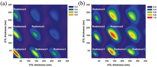
Table 1. Summarized radiance values of TEOLED calculated with the 1st, 2nd, and 3rd cavity orders.
3. Material technologies for high-efficiency TEOLEDs
3.1. HTL and ETL
HTLs and ETLs are essential for achieving highly efficient TEOLEDs. To optimize the device, the thickness of the HTL and ETL must be especially considered. As mentioned in 2.1.1, when designing the device, the proper resonance condition is needed due to the micro-cavity effect. This phenomenon is strong in the TEOLED structure because both its electrodes are reflective. The 2nd-order TEOLED structure is generally preferred over the 1st-order TEOLED structure because the 1st-order device is thin, which can affect the process yields. Because in an organic material, the hole mobility is higher than the electron mobility, a thick HTL and a thin ETL are often used. When choosing the proper HTL and ETL materials, several optical characteristics are needed. First, there should be no absorption in the visible wavelength region because light absorption in HTL and ETL causes low color purity and decreases the device efficiency. Second, the low refractive index of HTL and ETL materials makes them more efficient than materials with a high refractive index. In this regard, Fuchs et al. reported variations in TEOLED efficiency with HTL materials with different refractive indices [Citation65]. General TEOLEDs have a thick metal anode that causes surface plasmon loss between the metal anode and the adjacent HTL material due to the relationship between the refractive index and the electric permittivity (),
[Citation66]. As for the surface plasmon, the low refractive index of a material causes high electric permittivity and causes the surface plasmon mode to shift towards a smaller in-plane wavenumber [Citation66]. This phenomenon induces a change in the power dissipation. Moreover, a smaller refractive index reduces the surface plasmon loss, which increases the TEOLED efficiency. Thus, the TEOLED with a low-refractive-index HTL exhibited a higher EQE value than the TEOLED with high-refractive-index HTL. As for the ETL material, its refractive index also affects the device efficiency because the TEOLED cathode is composed of a thin metal, which can induce the surface plasmon effect with the dielectric material. Moreover, a low-refractive-index ETL is thicker than a high-refractive-index ETL, so it can increase the distance from the metal cathode. The use of a low-refractive-index ETL can enhance the device efficiency by decreasing the surface plasmon loss from the increased distance between the metal cathode and the emitter. Thus, the refractive index of HTL and ETL materials near the metal electrode must be considered.
3.2. Emissive layer (EML)
In OLEDs, EML is the most important layer for emitting the desired color with high efficiency. Since Tang et al. developed the initial EML structure, EML has been steadily developed. To achieve high efficiency, the electrical and material characteristics such as the charge balance, charge injection, dipole orientation, and photoluminescence quantum yield (PLQY) are key factors. In the case of EML, variation of the electrical characteristics has been reported in many researches, mostly variation of the host type such as into a bipolar host [Citation67,Citation68], a mixed host [Citation69,Citation70], and an exciplex host [Citation71]. Moreover, the dipole orientation measurement method and the use of the emitter dipole orientation have already been reported in many papers [Citation72–74]. Also, the shape of the emitter spectrum is the main factor in achieving a high-efficiency TEOLED. Because the micro-cavity effect enhances the spectral intensity of the resonance wavelength, the FHWM is reduced according to the emitter FWHM. Spectrally integrated emission enhancement can be represented as
(9)
(9) in which
and
are the resonant emission enhancement in the cavity medium and in the non-cavity medium, respectively [Citation75], and
and
are the emission spectrum width and the cavity mode width, respectively. Using Equation (9), the emitting material with a broad FWHM (a high
) will show lower enhancement than the narrow FWHM-based emitting materials. To confirm this effect, the optical simulation was performed using emitting materials with different FWHM values. Figure shows the emission spectra of two emitters, one of which has an FWHM of 72 nm (broad) and the other, an FWHN of 40 nm (narrow). The calculated TEOLED efficiency values with the two emitters are shown in Table . At the same thickness, the narrow FWHM emitter showed an about 5% greater increase in efficiency than the broad FWHM emitter in the 2nd-order cavity condition. As for the 3rd-order cavity condition, the calculated efficiency of the narrow FWHM emitter was almost the same, unlike in the 2nd-order cavity condition. On the other hand, the calculated efficiency of the broad FWHM emitter showed the opposite tendency due to the difference in the FWHM. Due to the low quantum efficiency of fluorescent materials, many researchers have studied phosphorescent and thermally activated delayed fluorescent (TADF) emitters (especially blue emitters), which harvest triplet excitons. However, they have a broad FWHM of over 60 nm due to the charge-transfer characteristic of the emitter [Citation76]. Recently, a blue TADF emitter with a boron acceptor was reported with a narrow FWHM due to the structural localized atom induced by the multi-resonance effect [Citation77]. Thus, applying an emitter with a narrow FWHM is a key factor in enhancing TEOLED efficiency.
Figure 5. (a) Spectra of the different FWHMs and radiance distributions of (b) the emitter with a broad FWHM and (c) the emitter with a narrow FWHM.
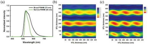
Table 2. Summarized radiance values of emitters with different FWHM.
3.3. Capping layer (CPL)
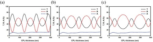
Compared to BEOLEDs, TEOLEDs have an additional important layer: CPL. Similar to the resonance wavelength condition between the thickness of the cathode and that of the anode in TEOLEDs, the thickness of the CPL is adjusted to match the resonance wavelength of the device. Figure shows the transmittance, reflectance, and absorbance spectra of the metal cathode at the red (610 nm), green (530 nm), and blue (460 nm) peak wavelengths with the variation of the CPL thickness. The spectral peak is varied according to the thickness of the CPL due to its different resonance conditions. These resonance conditions are caused by the partial reflection between the CPL and its interface, and this reflection phenomenon produces the resonance wavelength conditions such as the micro-cavity effect. To match the long-wavelength resonance conditions (red), a thick CPL is needed to fabricate the TEOLED. Thus, optimizing the CPL thickness with different colors is an important factor in optimizing the device efficiency. Another main factor of CPL is the refractive index value. In TEOLED, light is extracted through the ETL, cathode, and CPL. A high-refractive-index CPL increases the device efficiency in the normal direction [Citation78]. This phenomenon becomes stronger as the refractive index increases in common cathode metals such as Al and Ag. Among several CPL materials, the most commonly used materials are N,N′-Di(1-naphthyl)-N,N′-diphenyl-(1,1′-biphenyl)-4,4′-diamine (NPB), 4,4′-Cyclohexylidenebis[N,N-bis(4-methylphenyl)benzenamine] (TAPC), and Tris(4-carbazoyl-9-ylphenyl)amine (TCTA). However, they have a refractive index of about 1.8–1.9, which is too low to make them suitable for CPL application. A suitable alternative is metal oxide due to its high refractive index >2.0 [Citation79]. The most common metal oxide materials are molybdenum oxide (MoO3) and tungsten oxide (WO3), because they can be evaporated by the thermal evaporation method.
Figure 6. Transmittance (T), reflectance (R), and absorbance (A) of an Ag/CPL film after varying the CPL thickness for the (a) blue (460 nm), (b) green (550 nm), and (c) red (610 nm) colors.
3.4. Semi-transparent cathode
The semi-transparent conductive cathode is generally regarded as one of the key factors of microcavity-based TEOLEDs. To design high-performance microcavity-based TEOLEDs, a semi-transparent conductive cathode with low sheet resistance, high reflection, and low absorption is required. Also, a semi-transparent cathode should exhibit good electron injection into the adjacent ETL. The materials that are used to make a semi-transparent cathode in commercial TEOLEDs include the Mg-doped Ag (Mg:Ag) metal alloy with a 10:1 composition by volume due to the good electron injection property, high stability, and proper microcavity effect between the two electrodes [Citation80,Citation81]. The reported 20 nm-thick co-doped Mg:Ag (10:1) cathode showed a very high reflection of 41.7%, which resulted in a strong microcavity effect between the two reflective electrodes of the TEOLED [Citation81]. However, the Mg:Ag (10:1) cathode shows low transmittance (33.4%) due to the high extinction coefficient of Mg and exhibits high sheet resistance (33.4%), which affects the TEOLED efficiency [Citation81,Citation82].
Recently, S. Kwon et al. optimized the ratio of Ag in a co-doped Mg:Ag cathode to produce high-efficiency TEOLEDs [Citation81]. They reported that the higher ratio of Ag in the Mg:Ag alloy not only reduced the sheet resistance but also decreased the absorption property (Table ). The optimized Mg:Ag (1:10) cathode showed 5.2 Ω/sq sheet resistance, 41.4% average reflectance, 8.9% absorbance, and 49.7% transmittance. The sheet resistance and the optical properties of the Mg:Ag (1:10) cathode are better than those of the Mg:Ag (10:1) cathode. However, the Mg:Ag (1:10) cathode showed a poor electron injection property compared to the Mg:Ag (10:1) cathode. Also, the lower concentration of Mg in the Mg:Ag (1:10) cathode prevented the reaction of Mg with EIL (Mg, Cs, and LiF), which caused the poor electron injection from the cathode. On the other hand, the higher Mg concentration in the Mg:Ag (10:1) cathode reacts with the alkali metals (Mg, LiF, and Cs) and improves the electron injection property of the cathode. Yb is generally used as an efficient EIL due to its good electron injection stability under the operating and UV conditions compared to the Mg EIL (which was migrated into the cathode after UV exposure). The unwanted changes in the properties of the semi-transparent conductive cathode under the operating and UV conditions would reduce the device efficiency and lifetime. Also, the TEOLEDs with the 1:10 Mg:Ag composition showed strong pixel shrinkage and a short lifetime under UV exposure and the operating conditions. Particularly, in the case of the co-doped Mg:Ag film (1:10), the Mg atoms can be migrated toward the CPL under the UV irradiation or operating conditions due to its self-diffusion property, whereas the Ag atoms aggregated toward the EIL, which resulted in a poor electron injection property and reduced device efficiency [Citation82,Citation83] (Figure ). Although the Mg:Ag cathode-based TEOLED with a 1:10 ratio showed higher efficiency than that with a 10:1 ratio, the stability of this electrode under the operating conditions could be a major issue for real applications. Moreover, the TEOLED that contained a thin metal alloy cathode with low-extinction-coefficient materials such as Yb, Al, and molybdenum trioxide (MoO3) instead of Mg showed a performance similar to that of the Mg:Ag (10:1) cathode, but its efficiency and operating lifetime were still below the expectation [Citation84–86].
Figure 7. EDS data of the Mg:LiF (1:1, 2 nm) / Ag:Mg (10:1, 16 nm) / NPB (60 nm) cathode unit before and after UV irradiation. Reproduced from Ref. [Citation90].
![Figure 7. EDS data of the Mg:LiF (1:1, 2 nm) / Ag:Mg (10:1, 16 nm) / NPB (60 nm) cathode unit before and after UV irradiation. Reproduced from Ref. [Citation90].](/cms/asset/1f0e972f-0745-4244-a0da-b29e1b88c548/tjid_a_1876173_f0007_oc.jpg)
Table 3. Comparison of the electrical and optical properties of different cathodes for TEOLEDs.
To achieve high efficiency in TEOLEDs, a thermally evaporated pure metal (Ag) was also utilized as a semi-transparent cathode due to its higher conductivity and lower absorbance than those of other metals, including alkali metals. However, the uniformly thin Ag film cannot be deposited onto the conventional organic layer using thermal evaporation due to the agglomeration of Ag atoms, which deteriorates the electrical and optical properties of the semi-transparent conductive cathode. Also, the pure semi-transparent Ag cathode exhibited a poor electron injection property because of the large energy barrier between the work function of Ag and the organic ETL. Therefore, a multilayer cathode structure with two or more ultra-thin metal films has been reported as achieving a smooth morphology, low sheet resistance, and a good electron injection property. Especially, a thin metal layer with a surface energy similar to that of Ag (CsF/Yb/Ag, Al/Ag, Ge/Ag, etc.) has been used as a seed layer to overcome the agglomeration of Ag in the pure thin film [Citation87–92]. However, an additional seed layer increases the absorption property of the cathode, which leads to lower efficiency than with the Mg:Ag (10:1) cathode.
Among the reported multilayer cathode structures, the thin Ag film sandwiched between the organic charge transport layers showed not only low sheet resistance and improved optical properties but also high device efficiency and a good lifetime (Table ). Kim et al. recently reported a thermally stable semi-transparent pure Ag cathode by sandwiching a thin Ag film between phenanthroline-based organic layers for TEOLEDs [Citation93]. This cathode structure showed high transmittance (83.8% at 550 nm), low absorbance (7.65% at 550 nm), low sheet resistance (2.1 Ω/sq), and high thermal stability. They observed that both the organic wetting inducer and the CPL [1,4-bis(2-phenyl-1,10-phenanthrolin-4-yl)benzene (p-bPPhenB)] significantly stabilized the surface property of the Ag layer and prevented the agglomeration of the Ag atoms under high-temperature conditions by forming a coordination bond between the Ag atoms and the nitrogen atoms of p-bPPhenB. Also, to improve the electron injection from the pure Ag cathode, Kim et al. introduced the Ag-doped p-bPPhenB EIL in TEOLEDs, which shows good electron injection stability from the Ag cathode. Also, the green phosphorescent TEOLED with the p-bPPhenB:Ag/Ag/p-bPPhenB cathode showed very high current efficiency (167 cd/A) and a low driving voltage compared to the Mg:Ag (10:1) cathode (109 cd/A and 5.4 V).
The semi-transparent conductive metal cathode technology is important in improving the performance of the microcavity-based TEOLED. Several reports on the semi-transparent pure metal cathode indicated its comparable efficiency with the Mg:Ag (10:1) cathode, but further research is required to develop an optically and electrically stable thin metal cathode for display applications. The performance results of different groups of TEOLEDs are summarized in Table .
Table 4. Comparison of the performance results of TEOLEDs with different materials.
3. Conclusions and outlook
This paper summarized the optical design methods and material technologies for the improvement of the performance of TEOLEDs. Due to the use of reflective metal electrodes in TEOLEDs, an efficient device design method that uses accurate optical calculation is required to achieve high outcoupling efficiency. The basic optical design method that considers the microcavity effect and the calculation of optical losses showed a high-efficiency TEOLED design. Also, the optical design that used the Purcell factor showed an advanced solution for further improving the efficiency of TEOLEDs. Moreover, the electrically and optically efficient and stable semi-transparent metal cathode, the HTL and ETL with low refractive indices to reduce the surface plasmon loss caused by the metal electrodes, the narrow FWHM emitter, and the high-refractive-index CPL led to high outcoupling efficiency and good color purity. Thus, such materials are promising for the development of high-performance TEOLEDs.
Although proper optical calculation led to a high-efficiency TEOLED design, the development of stable organic materials and a semi-transparent metal cathode with suitable properties is still a challenging task. We believe that the TEOLED with a proper optical design method, a narrow FWHM emitter, a high-refractive-index CPL, and efficient HTL and ETL materials will be used in the development of next-generation solid-state lighting and display products.
Disclosure statement
No potential conflict of interest was reported by the author(s).
Additional information
Funding
Notes on contributors

Seong Keun Kim
Seong Keun Kim received his BS and MS degrees in Information Display from Kyung-Hee University in Seoul, South Korea in 2016 and 2018, respectively. He is working towards a PhD degree in Information Display at the same university. His research interests are modeling of devices, design and fabrication of OLEDs, and resonant-cavity devices.
Raju Lampande
Raju Lampande is a Research Professor at the Department of Information Display of Kyung Hee University in Seoul, South Korea. He received his MSc degree in Electronics from Rashtrasant Tukadoji Maharaj Nagpur University in India in 2006 and his PhD in Information Display from Kyung Hee University in 2016. His research interests are the development of OLEDs and QLEDs.

Jang Hyuk Kwon
Jang Hyuk Kwon is a Professor at the Department of Information Display of Kyung Hee University in Seoul, South Korea. He received his PhD degree in Chemistry from the Korea Advanced Institute of Science and Technology in South Korea in 1993. He was a Chief Researcher at Samsung SDI in South Korea in 1993–2005. His research interests are the development of organic materials for OLEDs, QLEDs, OPVs, and electrochromic devices.
References
- C.W. Tang and S.A. VanSlyke, Appl. Phys. Lett. 51 (12), 913–915 (1987).
- W. Helfrich and W.G. Schneider, Phys. Rev. Lett. 14 (7), 229–321 (1965).
- C. Wu, C. Chen, C. Lin, and C. Yang, J. Disp. Tech. 1 (2), 248–266 (2005).
- S. Chen, L. Deng, J. Xie, L. Peng, L. Xie, Q. Fan, and W. Huang, Adv. Mater 22, 5227–5239 (2010).
- Y. Kijima, N. Asai, N. Kishii, and S.-I. Tamura, IEEE Trans. Electron Devices 44 (8), 1222–1228 (1997).
- H. Kubota, S. Miyaguchi, S. Ishizuka, T. Wakimoto, J. Funaki, Y. Fukuda, T. Watanabe, H. Ochi, T. Sakamoto, T. Miyake, M. Tsuchida, I. Ohshita, and T. Tohma, J. Lumin 87–89, 56–60 (2000).
- S. Ono, K. Miwa, Y. Maekawa, and T. Tsujimura, IEEE Trans. Electron Devices 54 (3), 462–467 (2007).
- C.-L. Lin and Y.-C. Chen, IEEE Electron Device Lett 28 (2), 129–131 (2007).
- Y.-H. Tai, B.-T. Chen, Y.-J. Kuo, C.-C. Tsai, K.-Y. Chiang, Y.-J. Wei, and H.-C. Cheng, J. Display Technol. 1 (1), 100–104 (2005).
- B.-Y. Jung and C.-K. Hwangbo, J. Korean Phys. Soc. 48 (6), 1281–1285 (2006).
- P. Urquhart, Appl. Opt. 26 (3), 456–463 (1987).
- H.-C. Chen, J.-H. Lee, C.-C. Shiau, C.-C. Yang, and Y.-W. Kiang, J. Light. Technol. 24 (6), 2450–2457 (2006).
- A.A. Shcherbakov, A.V. Tishchenko, D.S. Setz, and B.C. Krummacher, Org. Electron 12 (4), 654–659 (2011).
- J. Park, Y.-Y. Noh, J.W. Huh, J.I. Lee, and H. Chu, Org. Electron. 13 (10), 1956–1961 (2012).
- J.-W. Shin, D.-H. Cho, J. Moon, C.W. Joo, J. Lee, J.W. Huh, S.K. Park, J.-H. Han, N.S. Cho, J. Hwang, H.Y. Chu, and J.-I. Lee, Opt. Lett. 39 (12), 3527–3530 (2014).
- E. Bodenstein, M. Schober, M. Hoffmann, C. Metzner, and U. Vogel, J. SID 26 (9), 555–560 (2018).
- X. Ke, H. Gu, X. Zhao, X. Chen, Y. Shi, C. Zhang, H. Jiang, and S. Liu, Optics Express 27 (16), A1014–A1029 (2019).
- K. Kang, J. Yoon, J. Kim, H. Lee, and B. Yang, Optics Express 23 (11), A709–A717 (2015).
- M. Slawinski, D. Bertram, M. Heukena, H. Kalisch, and A. Vescan, Org. Electron 12 (8), 1399–1405 (2011).
- J.-W. Kim, J.-H. Jang, M.-C. Oh, J.-W. Shin, D.-H. Cho, J.-H. Moon, and J.-I. Lee, Optics Express 22 (1), 498–507 (2014).
- A. Chutinan, K. Ishihara, T. Asano, M. Fujita, and S. Noda, Org. Electron. 6 (1), 3–9 (2005).
- Y. Deng, C. Keum, S. Hillebrandt, C. Murawski, and M.C. Gather, Adv. Optical. Mater, 2001642 (2020).
- Z. Bin, D. Shi, R. Su, W. Han, D. Zhang, and L. Duan, Sci. Bull. 65 (2), 153–160 (2020).
- J. Wang, H. Liu, S. Wu, Y. Jia, H. Yu, X. Li, and S. Wang, Chem. Eng. J 391, 123479 (2020).
- Y.-L. Wu, C.-Y. Chen, Y.-H. Huang, Y.-J. Lu, C.-H. Chou, and C.-C. Wu, Appl. Opt. 52 (22), E1–E6 (2014).
- H. Shin, J-H Lee, C-K Moon, J-S Huh, B. Sim, and J-J Kim, Adv. Mater. 28 (24), 4920–4925 (2016).
- X. Qiu, Y. Xu, C. Wang, M. Hanif, J. Zhou, C. Zeng, Y. Li, Q. Jiang, R. Zhao, D. Hu, and Y. Ma, J. Mater. Chem. C 7, 5461–5467 (2019).
- J.-X. Man, S.-J. He, D.-K. Wang, H.-N. Yang, and Z.-H. Lu, Org. Electron 63, 41–46 (2018).
- H. Ahn, H. Lee, J. Yang, and C. Lee, SID Symposium Digest of Technical Papers 43 (1), 1481–1483 (2012).
- S.-Y. Yu, J.-H. Chang, P.-S. Wang, C.-I. Wu, and Y.-T. Tao, Langmuir 30 (25), 7369–7376 (2014).
- D. An, H. Liu, S. Wang, and X. Li, Appl. Phys. Lett 114 (15), 153301 (2019).
- C.F. Madigan, M.-H. Lu, and J.C. Sturm, Appl. Phys. Lett. 76 (13), 1650–1652 (2000).
- J.F. Biegen, Opt. Lett. 19 (21), 1690–1692 (1994).
- J. Springer, A. Poruba, L. Müllerova, and M. Vanecek, J. Appl. Phys. 95 (3), 1427–1429 (2004).
- T.H. Gil, C. May, S. Scholz, S. Franke, M. Toerker, H. Lakner, K. Leo, and S. Keller, Org. Electron. 11 (2), 322–331 (2010).
- K. Suemori, S. Hoshino, N. Ibaraki, and T. Kamata, AIP Adv 7 (4), 045014 (2017).
- J.H. Im, K.-T. Kang, S.H. Lee, J.Y. Hwang, H. Kang, and K.H. Cho, Org. Electron 33, 116–120 (2016).
- M. Bertolotti, P. Masciulli, and C. Sibilia, Opt. Lett. 19 (11), 777–779 (1994).
- K. Mijuno, S. Ono, Y. Shibata, and I.E.E.E. Trans, Electron Devices 20 (8), 749–752 (1973).
- J. Krupk, A. Cwikl, M. Mrozowski, R.N. Clarke, and M.E. Tobar, IEEE T. Ultrason. Ferr 52 (9), 1443–1451 (2005).
- M.C. Gathera and S. Reineke, J. Photonics Energy 5, 057607 (2015).
- A. Salehi, X. Fu, D. Shin, and F. So, Adv. Funct. Mater. 29, 1808803 (2019).
- D.G. Deppe, C. Lei, C.C. Lin, and D.L. Huffaker, J. Mod. Optics 41, 325 (1994).
- E.F. Schubert, N.E.J. Hunt, M. Micovic, R.J. Malik, D.L. Sivco, A.Y. Cho, and G.J. Zydzik, Science 265, 943 (1994).
- W.C. Tien, L.Y. Chen, Y.W. Zeng, K.W. Chang, and A.K. Chu, IEEE Electorn. Lett. 51 (24), 2034–2035 (2015).
- T. Fleetham, J. Ecton, G. Li, and J. Li, Organ. Electron 37, 141–147 (2016).
- B.-T. Liou, M.-C. Tsai, Y.-H. Huang, F.-M. Chen, Y.-R. Lin, and Y.-K. Kuo, Proc. of SPIE 7935, 79315 (2011).
- M.J. Park, Y.H. Son, G.H. Kim, R. Lampande, H.W. Bae, R. Pode, Y.K. Lee, W.J. Song, and J.H. Kwon, Org. Electron 26, 458–463 (2015).
- M. Qian, X.-B. Shi, Y. Liu, Z.-M. Jin, X.-L. Wang, Z.-K. Wang, and L.-S. Liao, Org. Electron. 25, 200–205 (2015).
- W.L. Barnes, J. Mod. Opt. 45 (4), 661–699 (1998).
- H. Becker, S.E. Burns, and R.H. Friend, Phys. Rev. B 56 (4), 1893–1905 (1997).
- K.G. Sullivan and D.G. Hall, J. Opt. Soc. Am. B 14 (5), 1149–1159 (1997).
- M. Furno, R. Meerheim, S. Hofmann, B. Lussem, and K. Leo, Phys. Rev. B 85 (11), 115205 (2012).
- Y.H. Son, M.J. Park, R. Pode, and J.H. Kwon, ECS J. Solid State. Sc. 5 (1), R3131–R3137 (2016).
- A. Sharma and T.D. Das, Optik 221, 165350 (2020).
- A.-C. Wei and J.-R. Sze, Opt. Commun. 380, 394–400 (2016).
- M. Flämmich, M.C. Gather, N. Danz, D. Michaelis, A.H. Bräuer, K. Meerholz, and A. Tünnermann, Organ. Electron 11, 1039–1046 (2010).
- A. Dodabalapur, L.J. Rothberg, R.H. Jordan, T.M. Miller, R.E. Slusher, and J.M. Phillips, J. Appl. Phys. 80 (12), 6954–6964 (1996).
- H. Benisty, J. Opt. Soc. Am. A 15 (5), 1192–1201 (1998).
- K. Kang, Y. Lee, J. Kim, H. Lee, and B. Yang, IEEE Photonics J 8 (2), 1600519 (2016).
- D. Escudero, and D. Jacquemin, Dalton Trans. 44, 8346–8355 (2015).
- A. Obolda, Q. Peng, C. He, T. Zhang, J. Ren, H. Ma, Z. Shuai, and F. Li, Adv. Mater. 28 (23), 4740–4746 (2016).
- K.A. Neyts, J. Opt. Soc. Am. A 15 (4), 962–971 (1998).
- H. Cho, J. Chung, J. Song, J. Lee, H. Lee, J. Lee, J. Moon, S. Yoo, and N.S. Cho, Optics Express 27 (8), 11057–11068 (2019).
- C. Fuchs, P. Will, M. Wieczorek, M.C. Gather, S. Hofmann, S. Reineke, K. Leo, and R. Scholz, Phys. Rev. B 92, 245306 (2015).
- M.M. Braun and L. Pilon, Thin Solid Films 496, 505–514 (2006).
- S. Hu, J. Zeng, X. Zhu, J. Guo, S. Chen, Z. Zhao, and B.Z. Tang, ACS Appl. Mater. Interfaces 11 (30), 27134–27144 (2019).
- W. Li, J. Li, D. Liu, F. Wang, and S. Zhang, J. Mater. Chem. C. 3, 12529–12538 (2015).
- T.-H. Han, Y.-H. Kim, M.H. Kim, W. Song, and T.-W. Lee, ACS Appl. Mater. Interfaces 8 (9), 6152–6163 (2016).
- W. Song and J.Y. Lee, Appl. Phys. Lett. 106 (12), 123306 (2015).
- B. Zhao, T. Zhang, B. Chu, W. Li, Z. Su, H. Wu, X. Yan, F. Jin, Y. Gao, and C. Liu, Sci. Rep. 5, 10697 (2015).
- K. Kim, C. Moon, J. Lee, S. Kim, and J. Kim, Adv. Mater. 26 (23), 3844–3847 (2014).
- H.S. Yeon, H. Ha, H-G Kim, R. Kim, S-K Kwon, Y-H Kim, and J-J Kim, Adv. Mater 31 (21), 1808102 (2019).
- J. Song, K.-H. Kim, E. Kim, C.-K. Moon, Y.-H. Kim, J.-J. Kim, and S. Yoo, Nat. Commun. 9, 3207 (2018).
- R.H. Jordan, A. Dodabalapur, and R.E. Slusher, Appl. Phys. Lett. 69, 1997 (1996).
- Q. Zhang, B. Li, S. Huang, H. Nomura, H. Tanaka, and C. Adachi, Nature Photonics 8, 326–332 (2014).
- X. Liang, Z. Yan, H. Han, Z. Wu, Y. Zheng, H. Meng, J. Zuo, and W. Huang, Angew. Chem 130 (35), 11486–11490 (2018).
- G.Z. Ran, W.Q. Zhao, G.L. Ma, L. Dai, and G.G. Qin, J. Opt. A: Pure Appl. Opt 8, 733–736 (2006).
- B. Hu, H. Chen, C. Li, W. Huang, and M. Ichikaw, Appl. Opt. 59 (13), 4114–4121 (2020).
- S. Hofmann, M. Thomschke, B. Lussem, and K. Leo, Optics Express 19, A1250 (2011).
- S.K. Kwon, E.H. Lee, K.S. Kim, H.C. Choi, M.J. Park, S.K. Kim, R. Pode, and J.H. Kwon, Optics Express 25, 29906–29915 (2017).
- S.K. Kwon, J.H. Baek, H.C. Choi, I.B. Kang, S.K. Kim, R. Pode, and J.H. Kwon, IEEE Electron Device Lett. 39, 1536–1539 (2018).
- S.K. Kwon, J.H. Baek, H.C. Choi, S.K. Kim, R. Lampande, R. Pode, and J.H. Kwon, RSC Adv. 9, 42561 (2019).
- M.J. Park, S.K. Kim, R. Pode, and J.H. Kwon, Organ. Electron 52, 153–158 (2018).
- M.G. Song, K.S. Kim, H.I. Yang, S.K. Kim, J.H. Kim, C.W. Han, H.C. Choi, R. Pode, and J.H. Kwon, Org. Electron. 76, 105418 (2020).
- W.F. Xie, K.C. Lau, C.S. Lee, and S.T. Lee, Thin Solid Films 515, 6975–6977 (2007).
- M.T. Lee and M.R. Tseng, Curr. Appl. Phys. 8, 616–619 (2008).
- H. Peng, J. Sun, X. Zhu, X. Yu, M. Wong, and H.S. Kwok, Appl. Phys. Lett. 88, 073517 (2006).
- M.T. Chan, S.L. Lai, M.K. Fung, S.W. Tong, C.S. Lee, and S.T. Lee, Appl. Phys. Lett. 82, 1784 (2003).
- C.J. Lee, R.B. Pode, J.I. Han, and D.G. Moon, Appl. Phys. Lett. 89, 253508 (2006).
- J. Zhang, D.M. Fryauf, M. Garrett, V.J. Logeeswaran, A. Sawabe, M.S. Islam, and N.P. Kobayashi, Langmuir 31, 7852–7859 (2015).
- V.J. Logeeswaran, N.P. Kobayashi, M.S. Islam, W. Wu, P. Chaturvedi, N.X. Fang, S.Y. Wang, and R.S. Williams, Nano Lett 9, 178 (2009).
- S.K. Kim, R. Lampande, and J.H. Kwon, ACS Photon. 6, 2957–2965 (2019).
- J. Lee, T. Gang, J. H. Kwon, S. Lee, J. Jung, and E. Kim, KR 1,006,564,900,000 (2006).
- H. Fukagawa, T. Oono, Y. Iwasaki, T. Hatakeyama, and T. Shimizu, Mater. Chem. Front. 2, 704–709 (2018).
- M.J. Park, G.H. Kim, Y.H. Son, H.W. Bae, J.H. Kong, and J.H. Kwon, Optics Express 22 (17), 19919–19929 (2014).
- J.-J. Lee, P. Li, H.-T. Kung, and Z.-H. Lu, J. Appl. Phys. 125, 144501 (2019).
- X. Shi, J. Wang, J. Liu, S. Huang, X. Wu, C. Chen, J. Lu, Y. Su, Y. Zheng, W.Y. Kim, and G. He, Org. Electron 15, 864–870 (2014).
- H. Cho, C.W. Joo, B.-H. Kwon, N.S. Cho, and J. Lee, Org. Electron. 62, 72–76 (2018).
- G. Xie, K. Fehse, K. Leo, and M.C. Gather, Phys. Status Solidi A 211 (5), 1168–1174 (2014).
- S.H. Cho, S.W. Pyo, and M.C. Suh, Synth. Met. 162 (3–4), 402–405 (2012).
- E. Najafabadi, K.A. Knauer, W. Haske, and B. Kippelen, Org. Electron. 14, 1271–1275 (2013).
- K.A. Knauer, E. Najafabadi, W. Haske, and B. Kippelen, Appl. Phys. Lett. 101, 103304 (2012).
- Z. Wu, Y. Zhai, R.X. Guo, and J. Wang, J. Lumin. 131, 2042–2045 (2011).
- Y. Liu, T. Ding, X. Chen, F. Bai, A. Genco, H. Wang, C. Chen, P. Chen, M. Mazzeo, Y. Zhang, and Y. Duan, Adv. Opt. Mater. 8 (15), 2000206 (2020).