
 ?Mathematical formulae have been encoded as MathML and are displayed in this HTML version using MathJax in order to improve their display. Uncheck the box to turn MathJax off. This feature requires Javascript. Click on a formula to zoom.
Abstract
The principal causes of the poor picture quality on active matrix organic light-emitting diode (AMOLED) displays, operating under extremely low brightness and gray-scale conditions, were analyzed and verified by measuring and modelling of the electrical simulations. Through the analysis, it was found that the deteriorated picture quality was induced by a delayed saturation voltage, which means the electric potential difference between the initial voltage applied to the anode of the OLED (Vinit) and the OLED saturated voltage (Vsat) for emission. This is because the deviations of pico-ampere-level currents and delayed OLED charging prior to light emission increased the saturation voltage when there were low driving currents. Thus, we optimized the voltage by increasing Vinit from −4.5 to −2.7 V, effectively eliminating image deterioration by reducing the OLED charging delay. Thus, the proposed approach opens up advancements of obtaining superior picture quality with ultra-low luminance, even in the dark illuminance environments. We discuss how OLED picture quality may be enhanced under low brightness, including the driving methods, design considerations, and processes involved.
1. Introduction and motivation
The active matrix organic light emitting diode (AMOLED) display is a market-leading technology that overwhelms other flat panel display technologies and is employed in a variety of fields, from the large size display applications such as TVs and signages, along with small displays such as those of smartphones. Since the late 2000s, the AMOLED displays have been extensively commercialized; currently, the mobile display market employs flexible (curved and foldable) AMOLED displays; the demand for small- and medium-sized displays for smartphones is increasing [Citation1,Citation2].
Because of recent trends of smartphone devices depending on increasement of the usage time in the low brightness mode and the rapid improvement of the shooting performance in the low ambient light environment of the camera, the expression accuracy and picture quality of the display devices at the extremely-low luminance have become an important evaluation criterion of the display performance.
Fig. S1 shows the latest smartphones, which have several cameras that enhance image capture performance. High-end smartphones have several cameras on the back that can operate in various environments. A high-end smartphone using an AMOLED has recently been released, and shows markedly improved image capture performance even at low illuminance [Citation3]. Advanced mode for low-light shooting called ‘Night vision’ improves image quality. A picture taken in low light with night vision mode disabled appears gray; with night vision enabled, the picture is much brighter (Figure ).
Figure 1. The picture quality comparison (a) Without advanced function in low light, (b) With advanced function in low light called as ‘Night Vision’.
Because of the enhancement of camera shooting performance in low-light environments, this device requires the acquisition of more sophisticated gradations images in low light, which means that the performance improvement for the precise expression of the display in low luminance is also required.
Moreover, with the increase in usage time in very dark situations, such as watching a video in a dark bedroom before falling asleep, the lowering brightness of display is indispensable [Citation4]. As a result, high-quality imaging at ultra-low illuminance is an important aspect of display performance [Citation5,Citation6]. In addition, smartphones are equipped with features that can reduce eye fatigue according to the user environment. In accordance with studies on the effects to sleep, eye strain, and human performance etc. [Citation7–10], recent smart devices have provided with functions that help the users to take comfortable biological night’s sleep in a dark illuminance environment, such as for reducing or controlling the light-emitting amount of the short wavelength (blue light) to reduce fatigue of the eyes separately [Citation11]. Among the various factors that cause such eye fatigue and other side effects, the luminance of the display is the key sensitive element. Most smartphone users reduce brightness to minimize eye fatigue in low illuminance conditions.
Nevertheless, the AMOLED panel should support the precise luminance expression and 24 bit full color of 255 gray for implementing the excellent picture quality in this situation [Citation4–6]. However, in the high-resolution range of full High-definition+ (FHD+; 400 pixels per inch [ppi]) to quadruple high-definition+ (QHD+; 550 ppi), the current required is only tens of nano-amperes at 500 nit. Thus, the current is at the pico-ampere scale or below when the peak brightness is 2 nit. In addition, since it is necessary to further lower the amount of current to express low luminance under 32 gray scales, there is a limitation to improvement in adjustment of the compensation circuit for each pixel. Therefore, some studies also show the methods which can be compensated outside the panel have also been applied for overcoming the limit of the pixel compensation circuits [Citation12,Citation13].
However, even after applying compensation outside and inside the panel to improve grayscale expression, the method used to drive the AMOLED display cannot ensure good image quality at extremely low luminance, because the current controlled by the driving thin-film transistors (TFTs) is affected by the square terms of the potential difference between the gate and the source. Furthermore, it has been more difficult to precisely control the gray scale on the AMOLED display because of the sharply decreased the current in unit pixel as increasing resolution over the 400–600 ppi and drastically increased OLED efficiency [Citation14,Citation15] and the improvement of the panel power consumption.
Given these demanding display driving conditions, even if the image taken with an excellent image with an advanced camera on the smartphone, it may not be precisely implemented in the display. As a result, the deteriorated picture quality in the panel stands out severely at the extremely low luminance and then vendors of the AMOLED panel have confronted the large yield drop. To solve these problems, some researches that propose new internal [Citation16–23] or external [Citation13,Citation24] compensation circuits or improving uniformity of TFT and OLED processes [Citation25,Citation26] have been reported. In other ways, researches suggesting an improving operation method for the reduction of the current sensitivity [Citation27] or have proposed the screening method during the processes [Citation28,Citation29].
However, these methods still have not solved the deterioration of picture quality at very low luminance (< 2 nit). Various analyses on the causes of picture quality deterioration and its improvements are still needed to develop new technologies of backplane [Citation30].
2. Types of display quality deterioration
At low brightness, the deteriorated AMOLED picture quality phenomenon appears as three kinds of failure modes which consist of ‘Stain (Mura)’, ‘Bluish Motion Blur’, and ‘Contour Image and Gamma Crush’. Prior to the analysis of low-luminance stain, the distinction of stains is proceeded to analyze diverse causal factors. The types of stains, as shown in Fig. S2, can be divided based on luminance mode and gray scale level. (The luminance or brightness mode refers to the function to be divided into several steps by the luminance of 255 gray (white) by ambient illuminance and is also referred to as dimming mode.) The stains can be classified into four types according to gray level and brightness mode. In this study, except other three types of stains beyond the mid gray and luminance which are caused by various reasons from such as OLED process [Citation31–33], IR drop [Citation34–37] or TFT process [Citation25]. We focus on the stain () that can occur in 10 gray scale images with 500-nit brightness, and in 32 gray scale images with 2-nit brightness. At extremely low brightness, luminance is defined as follows:
(1)
(1) Where L is the luminance of each gray scale, the Lpeak is a peak luminance of the brightness mode, G is gray scale, and γ is the gamma factor (usually 2.2) of the display panel [Citation38–40]. The luminance of 3 gray in the 500 nit mode is only 0.028 nit; that of a 32 gray scale image under 2-nit brightness is also very low, at 0.02–0.03 nit (Figure and S2). Fig. S11 shows transfer characteristics of the driving TFTs. As this characteristic implies, the current value for the low grayscale is significantly low with a sub-threshold current. As a result, the image quality of the low brightness deteriorated.
Deteriorated phenomena at low luminance, ‘Stain (Mura)’, ‘Bluish Motion Blur’, and ‘Contour Image and Gamma Crush’ as demonstrated Figures . The panels have a featuring that the edge areas of the panel are brighter than center areas shown in Figure . Moreover, the color of low gray bar changes into bluish when it moves at low brightness mode over black background shown in Figure and it looks like a localized bluish blur of low gray bar changes into bluish when it moves at low brightness mode over black background shown in Figure and it looks like a localized bluish blur. Another phenomenon is low gray contour and crush shown in Figure . The contour lines appear in the area expressed with low luminance at ultra-low brightness mode shown in Figure (b). Furthermore, some of the ultra-low luminance areas cause gamma crush symptoms that cannot be expressed as shown in Figure (c).
Figure 2. Example image of failure mode phenomenon on the 6.39’ FHD+ AMOLED display panel at 0.02 nit (32 gray at 2 nit, 3 gray at 500nit) with the luminance difference where the panel edge areas are much brighter than the center area.
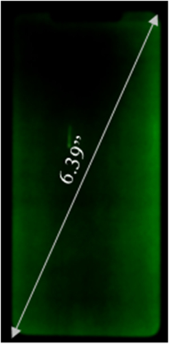
Figure 3. Bluish blur phenomenon at the low brightness mode. (a) Evaluation method of failure. The image quality was evaluated by scrolling the gray bar. (b) Failure phenomenon of the bluish blur in 6.47’ FHD+ AMOLED Panel. The color of gray bar changed into locally bluish while moving the bar from top to bottom.
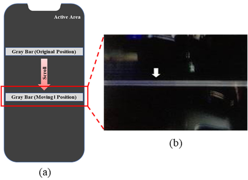
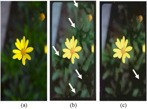
Figure 4. Contour and gamma crush phenomenon of the 5.99’ QHD+ AMOLED display panel. (a) Original image, (b) Contour image, (c) Low gray gamma crush (LGGC) image. This phenomenon appears in 2 nit brightness mode.
Via all the phenomena shown in Figures , we hypothesized that an extremely low current will not uniformly support the pixels, leading to a deterioration of display quality.
3. Major factors leading to picture quality degradation
To analyze the degradation of display quality, the CA-310 luminance meter (Konica Minolta) was used in our experiments. The measurement results of gamma in 2 nit mode are shown in Fig. S3(a) and (b). The gray scale is not precise under 40 grays in the 2-nit mode. We term this ‘Low Gray Gamma Crush (LGGC)’. Similarly, the gray scale steps are absent below 35 grays [Fig. S3(c)]. We defined this phenomenon as ‘Low Gray Gamma Crush (LGGC)’.
This failure occurs the same result that the step of the gray scale does not represent under 35 gray shown in Fig. S3(c). The luminance required for the actual emission is almost close to the black and it should be implemented through a low current of the pA level. That means charging of the OLED capacitance and increasing anode voltage to emit the light is conducted to small current, calculated as follows:
(2)
(2)
(3)
(3) Where, QD and iD are the charge and current for specific luminance, tE is emission time (frame time), COLED is OLED capacitance, and ΔVc is the charging voltage. The voltage ΔVC required for light emission is calculated as follows:
(4)
(4) The voltage ΔVC, which should be charged for light emitting, is as follows:
(5)
(5) As an example, when the current for low luminance is 40 pA per unit pixel, COLED is 100 fF, and ΔVC is 4 V, it takes 10 ms in order that the unit pixel is to be charged with a turn-on voltage (Vto) and saturated voltage (Vsat) state for reliably light emission. It means that the brightness might be changed by fluctuations in factors such as OLED capacitance, resistance, or OLED turn-on voltage during a time amounting to 60% of the 16.7 ms as 1 frame time on 60 Hz due to the deviation of turn-on and static emission for each pixel. Consequently, the pixels vary in terms of turn-on time and static emission-voltage level.
This could be verified by comparing OLED capacitance and voltage (CV) characteristics with the initial current of the light emitting. When the deviation occurs during charging from the initial voltage (Vinit) to the Vto and Vsat of OLED, the OLED emitting time in a frame time is changed. As a result, the amount of luminance and the performance of each pixels are different. It can be explained with the equation (5).
Besides, it can be verified via analysis of the OLED bias operation. Figure shows the operation sequence by the period according to the diode operating characteristics of the OLED. Figure (a) and (b) show that the sequence can be divided into three periods. In period I, the OLED does not flow current in this interval where the reverse bias is applied, according to increasing the voltage, the charges are accumulated to the COLED and the voltage of the anode begins to rise from Vinit. In period II, the voltage charged to the COLED rises to the Vto of the OLED, and the current begins to flow through it. Also, during period II, the anode voltage to reach the gray brightness is raised to the Vsat (OLED forward voltage for emitting the gray current, I3gray) described in Figure (b) and (c). In period III, the anode reaches a corresponding voltage and emits light while flowing the uniform current during the light-emission period. In periods I and II, the slope is a factor that can cause deviations affected by the current amount of the unit pixels, the capacitance of the OLED, and wiring resistance. The charging delay may also vary. During periods I and II, luminance differences cause a stain.
Figure 5. OLED operation sequence schematics according to specific period. (a) Change of the conduction in equivalent circuit by period, (b) OLED I-V Curve by operating period, and (c) Anode voltage transition sequence.
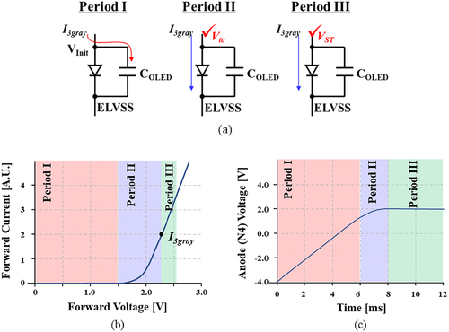
Fig. S4 shows how the variation of the anode voltage changes according to these factors in each period. Fig. S4(a) is a graph showing Vto change of the OLED, and it is possible to be changed with positive or negative shift compared to the typical value.
The change of the Vto, as well as to predict when the current flows to the OLED, determines the Vsat of the anode for the corresponding brightness. When the turn on voltage of the OLED is negative shift, the Vsat is lowered, as shown in Fig. S4(b), which can be expected to improve uniformity by the effect of shortening saturation time. Early stabilization time (voltage saturated time) through voltage saturation occurs when, as well as the negative shift of the Vto of OLED, the amount of current in the unit pixel increases or COLED decreases, as shown in Fig. S4(c).
On the other hand, in the case of a decrease in the amount of unit pixel current or an increase in COLED, the stain and LGGC phenomenon is deteriorated because of the stabilization time delay consequently. Based on this explanation, we can find out an important fact through comparing the non-uniformity in low luminance with the results of the ELVSS (OLED cathode voltage) rising simulation in Fig. S5(a) and (b). The IR (current–resistance) rising in ELVSS voltage depends on the variation of the cathode resistance, edge areas of the panel at the adjacent power line have relatively small resistance in the increase the ELVSS voltage slightly. This distribution of the cathode voltage shows that the ELVSS of the edge region is relatively lower than center, and the ELVSS voltage and Vsat increases gradually from the center to edge.
As you can see in Fig. S5, the IR rising model shows ELVSS power line connected from pan-el edge (bezel area) [Citation39,Citation41]. As a result, the ELVSS voltage of center area rises higher than the panel edge. According to ELVSS rising, the voltage applied between OLED anode and cathode decreases; the luminance of the panel center area also decreases. So, it is possible that the failure phenomenon in Figure can be explained.
Consequently, this phenomenon that edge areas are relatively brighter than center areas, which can verify similar feature of ELVSS IR rising simulation result.
As shown in Table , this can be explained by the significantly decreased red and green responses at low luminance. Therefore, it shows that the low-luminance bluish blur phenomenon is caused by a relative lack of light emitting of green OLED devices. In the case of red or blue device, the amount of current required in the unit pixel easy to charge for the OLED Vsat can be easily emitted corresponding color. So, it shows that the color change is dominant in the blue saturation and lack of green light emitting. In particular, the response characteristic of the mono color of green as described in Table . shows a tendency to decrease sharply as the brightness is lowered, it can attribute that due to the above-mentioned cause.
Table 1. Luminance ratio between 1st and 3rd frame at 2 nit mode
By the reduction of luminance, the response ratio of mid gray level for red and green mono color decreases more rapidly than blue color. So, the color of gray bar change into bluish. This implies that the current required by blue pixels is higher than that needed for red and green pixels, and the time to reach the turn-on voltage of blue OLEDs is relatively short. Therefore, response characteristic shown Fig. S6 is determined by the OLED charging time. Moreover, in contrast, the lack of charging in anode of each pixel leads to contour effect on the panel. That is, the contour lines appear in the image consisted of green mainly due to low driving current.
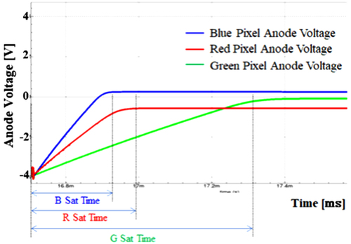
The change of the original color implies current deviation of red, green, and blue pixel. Figure represents the anode voltage of the red, green, blue OLED in the emission period. According to the simulation result, the Vto between the R/G/B is different, and blue and red pixel is charging quickly in contrast to green, as a result it can be explained that the reason of the color motion blur because of emitting time difference. Even though the response time (motion blur) of the AMOLED display depends on the TFT hysteresis characteristics [Citation42–44], in case of ultra-low brightness, the motion blur phenomenon depends on this explanation.
Figure 6. The simulation result of the anode voltage for emitting R/G/B pixels, respectively. The anode voltages rise to Vsat from Vinit and it shows the difference of saturation time of red, green, and blue.
In the case of deteriorated picture quality caused by the very low current, it is possible to verify through the mechanism shown in Figure . As with the 7 transistor and 1 capacitor (7T1C) of Figure (a), in the case of general compensation pixel circuits applied to the AMOLED display, (1) initialization, (2) Vth sampling (sensing), and (3) the light emission operation is performed, in particular, the application of the initialization period to delete the light emitting data of the previous frame is indispensable. For example, in the case of p-type Metal Oxide Semiconductors (pMOS) 7T1C pixels, it resets the gate node and storage capacitor of the driving TFT through the Vinit voltage and at the same time resets the anode (N4) voltage. After sampling period, N4 maintains the Vinit voltage in a floating state, and is then emitting as the current is applied to the OLED in the emission period.
Figure 7. Mechanism of ultra-low luminance stain. (a) Schematics of 7T1C pixel, (b) Anode (N4 in (a)) node change from Vinit to Vsat, and (c) Schematic of driving TFT gate and OLED anode node voltage according to compensation sequence.
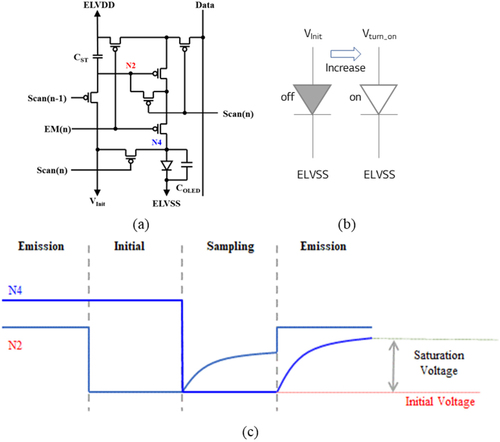
Generally, Vinit voltage is applied to the negative voltage, and the increase in voltage from Vinit to Vto of OLEDs for the light emission is required, but the charging through the non-uniform low current of the low-gray brightness does not perform efficiently, as well as the light emission for the implement for the high quality of the display image improperly. The increased period of the anode voltage in Figure has the slope period depending on the R/G/B current, it can be explained as the part where the anode voltage fluctuations are induced, during the change as depicted in Figure (b). Simultaneously, the light emission begins at the starting point of the Vinit for the anode voltage in Figure (c). It increased up to the saturation value after turn-on, and then gray level can be expressed according to the current of corresponding brightness.
Therefore, the major reason for poor picture quality is the low current at low luminance, and the high potential difference of the OLED.
4. Enhancement of picture quality and consideration
Due to the low current applied to implement a very low brightness, the OLED could be turned-on in different characteristics to reach the Vsat, which is directly induced by a difference in brightness, it was explained that the stain can occur. At low brightness, it is essential to reduce the current, but it must consider the detailed operation of the pixel for the picture quality enhancement. For comprehension of this explanation from the other pixel circuits shown in Fig. S7, S8, and S9 such as 7T1C, 6T1C (pMOS) and 4T2C (nMOS) circuits, the Cst and driving TFT gate node are initialized and the anode voltage is also initial voltage or reference voltage simultaneously.
To reduce the negative effect generated by the low current, increasing the Vinit applied to the anode is an effective way to reduce the charging delay that occurs before the OLED emits light. As a result, it is possible to reduce the delay deviation required for charging. This charging delay is a factor of deviation occurring on the operation of the pixel, decreasing electrical potential applied to the OLED can be expected that shorten the saturation time to improve the picture quality. Therefore, the minimizing electric potential of anode help the panel improved for high picture quality at ultra-low luminance condition. Based on this explanation, in addition to the methods presented above, various methods as shown in Table have been proposed to improve image quality even in a low current.
Table 2. Recommendation of the enhancement methodologies for low brightness stain
To explain in detail, when expressing a low-grayscale, in order to improve the charging delay, the current needs to increase by reducing the OLED efficiency or adjusting the light emitting time through PWM (Pulse Width Modulation). Increasing a thickness of the OLED cathode layer is the simple method because the thickness increment induces the drop of OLED’s efficiency and wiring resistance simultaneously. By increasing the cathode thickness, transmittance of OLED has decreased. As a result, the OLED efficiency also has decreased. Furthermore, by increasing the cathode thickness, the sheet resistance of cathode has been decreased. Therefore, increment of cathode layer shows effective way for improving the failure phenomenon.
Moreover, it is possible to reduce the RC component by reducing the parasitic capacitance through the thickness increase of the OLED or the resistance. Increment of the organic layer (dielectric material of capacitance) between anode and cathode reduces COLED. By decreasing aperture ratio of OLED, it can reduce the capacitance (area of capacitance) for charging. In addition, applying the low resistivity materials and increasing the thickness of metal layer has recommend to reducing the wiring resistance. Furthermore, it is also able to reduce the electrical range of the electrical voltage by lowering the turn-on voltage of the OLED as well [Citation45,Citation46]. Also, for applying PWM to emit light at partial time of the unit frame, it is possible to improve by increasing the amount of current.
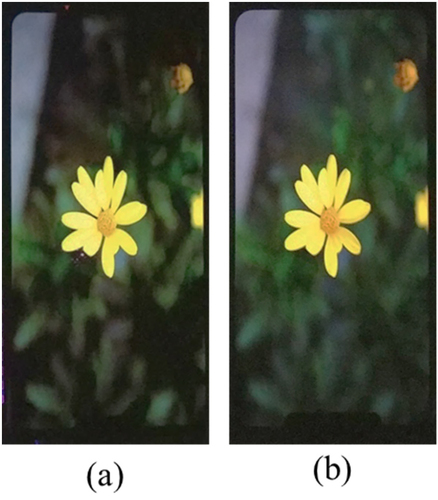
However, reducing the light emitting area for COLED reduction is also limited by causing a re-duction in the lifetime of the OLED accordingly because of increasing current density. Besides, the organic layers can reduce the COLED through the thickness upward, but this also results in a variety of side effects, such as OLED efficiency reduction, increase in operating voltage, light intensity reduction, so it should be selected by considering these conditions together for the manufacturing of the display panel. Fig. S10 shows lowering the ELVSS leads to the saturation time reduction through decreasing Vsat, thus it can explain the same effect on minimizing voltage gap between Vinit and Vsat. As a result, it was possible to significantly enhance the picture quality as shown in Figure by applying optimized Vinit from – 4.5 V to −2.7 V.
Figure 8. Improve result by minimizing of electric potential between Vinit and Vsat (a) Failure image on display panel, (b) Enhancement image on 6.47’ FHD+ AMOLED display panel by optimizing Vinit.
5. Conclusion
In this study, the deterioration phenomena of picture quality on AMOLED display at ultra-low luminance was defined and analyzed via measurement with actual display panel and its simulation results. As a result, it was found that the representative cause of this picture quality deterioration is voltage charging deviation from the low current. To solve this problem, a simple method was proposed which is optimization of the driving voltage by minimizing electric potential between Vinit and Vto/Vsat of anode. Additionally, based on the phenomena analysis, various methodologies have been suggested capable of realizing low luminance images in high quality even with the low currents. These methods are easy to apply in the display industry while overcoming limitations with acquiring high picture quality.
tjid_a_1923581_sm2796.docx
Download MS Word (1.3 MB)Disclosure statement
No potential conflict of interest was reported by the author(s).
Additional information
Funding
Notes on contributors

Se Hwan Na
Se Hwan Na is currently pursuing the Ph.D. degree with the School of Electrical and Electronic Engineering, Yonsei University, Seoul, South Korea. And he is also currently a Senior Research Engineer as mobile OLED panel design with the Mobile Business Unit, LG Display, Paju, Korea.

Won Kyung Min
Won Kyung Min is currently a Ph.D. candidate in the same institute. He has been conducting research on CMOS and low power electronics based on n- and p-type oxide and oxide semiconductor-based sensors such as photosensors and biosensors.

Do Hyung Kim
Do Hyung Kim received B.S. and M.S. degree with School of Electronic and Electrical Engineering, Hongik University, Seoul, South Korea, in 2003 and 2005, respectively. He is currently a Manager of Mobile Panel Design Team with the Mobile Business Unit, LG Display, Paju, Korea.

Han Wook Hwang
Han Wook Hwang received the Ph.D. degree from the School of Electrical and Electronic Engineering, Yonsei University, Seoul, South Korea, in 2019. He is currently a Vice President of the Mobile Business Unit, LG Display, Paju, Korea. His research interests are LTPS and oxide TFT for AMOLED mobile display applications.

Yong Min Ha
Yong Min Ha received M.S. and Ph. D. degree from Department of Electrical Engineering, Korea Advanced Institute of Science and Technology (KAIST), Daejeon, South Korea, in 1990 and 1994, respectively. He is currently an Executive Vice President of the Mobile Business Unit, LG Display, Paju, Korea.

Hyun Jae Kim
Hyun Jae Kim received the Ph.D. degree from the Department of Materials Science and Engineering, Columbia University, New York City, NY, USA, in 1996. Since 2005, he has been a Professor with the Faculty of the School of Electrical and Electronic Engineering, Yonsei University, Seoul, South Korea.
References
- S. Hong, C. Jeon, S. Song, J. Kim, J. Lee, D. Kim, 25.4: invited paper: development of commercial flexible amoleds. SID Symposium Digest of Technical Papers; 2014, Wiley Online Library 45, 334–337 (2014).
- “Foldable OLEDs: introduction and market status.”, oled-info.com, [Online] Available: https://www.oled-info.com/foldable-oleds (accessed Aug. 10, 2020)
- R. Triggs. “How are smartphone cameras becoming so good in low light?”, androidauthority.com, [Online] Available: https://www.androidauthority.com/low-light-phone-cameras-1037738 (accessed July 22, 2020)
- R.M. Soneira. “Watching Displays at Night.”, displaymate.com, [Online] Available: http://www.displaymate.com/Displays_At_Night_f_1.htm (accessed. Aug. 7, 2020)
- R.M. Soneira. “Galaxy S20 Ultra OLED Display Technology Shoot-Out.”, display mate.com, [Online] Available: http://www.displaymate.com/Galaxy_S20_ShootOut_1U.htm (accessed. Aug. 7, 2020)
- R.M. Soneira, “iPhone X OLED Display Technology Shoot-Out”, display mate.com, [Online] Available:http://www.displaymate.com/iPhoneX_ShootOut_1a.htm(accessed Aug. 10, 2020)
- A.U. Viola, L.M. James, L.J. Schlangen, and D.-J. Dijk, Blue-enriched white light in the workplace improves self-reported alertness, performance and sleep quality, Scand J Work Environ Health 34 (4), 297–306 (2008).
- S.W. Lockley, E.E. Evans, F.A. Scheer, G.C. Brainard, C.A. Czeisler, and D. Aeschbach, Short-wavelength sensitivity for the direct effects of light on alertness, vigilance, and the waking electroencephalogram in humans, Sleep 29 (2), 161–168 (2006).
- C. Cajochen, S.B.S. Khalsa, J.K. Wyatt, C.A. Czeisler, and D.-J. Dijk, EEG and ocular correlates of circadian melatonin phase and human performance decrements during sleep loss, Am J Physiol Regul Integr Comp Physiol 277 (3), R640–R649 (1999).
- S. Benedetto, A. Carbone, V. Drai-Zerbib, M. Pedrotti, and T. Baccino, Effects of luminance and illuminance on visual fatigue and arousal during digital reading, Comput Human Behav 41, 112–119 (2014).
- R.M. Soneira. “Light Spectra for the Samsung Galaxy S20 Ultra.”, displaymate.com, [Online] Available: http://www.displaymate.com/Spectra_52U.html (accessed Aug. 7, 2020)
- K. Oh, S.-K. Hong, and O.-K. Kwon, A luminance compensation method using optical sensors with optimized memory size for high image quality AMOLED displays, J Opt Soc Korea 20 (5), 586–592 (2016).
- H.-J. In, and O.-K. Kwon, External compensation of nonuniform electrical characteristics of thin-film transistors and degradation of OLED devices in AMOLED displays, IEEE Electron Device Lett 30 (4), 377–379 (2009).
- M.R. Nagar, R.A.K. Shahnawaz, J.-T.L. Yadav, and J.-H. Jou, Nanocomposite Electron-Transport Layer Incorporated Highly Efficient OLED, ACS Appl Electron Mater 2 (6), 1545–1553 (2020).
- W. Youn, J.W. Lee, H. Yu, and D.Y. Kim, Effect of Refractive Index Contrast on Out-Coupling Efficiency of Corrugated OLEDs using Low-Refractive-Index LiF Interlayer, ACS Appl Electron Mater 2 (7), 2218–2223 (2020).
- R. Dawson, Z. Shen, D.A. Furst, S. Connor, J. Hsu, M.G. Kane, R.G. Stewart, A. Ipri, and C.N. King, The impact of the transient response of organic light emitting diodes on the design of active matrix OLED displays, International Electron Devices Meeting 1998. Technical Digest (Cat. No.98CH36217), IEEE, 875–878 (1998).
- Y. Sohn, G. Moon, K. Choi, Y. Kim, and K. Park, Effects of TFT mobility variation in the threshold voltage compensation circuit of the OLED display, JID 18 (1), 25–30 (2017).
- H.-k. Chung, Y.-W. Kim, C.-y. Oh, O.-K. Kwon, and S.-M. Choi, Organic light emitting device pixel circuit and driving method therefor, Google Patent (Aug. 19, 2008).
- B. Liu, D. Ding, T. Zhou, and M. Zhang, P-53: A Novel Pixel Circuit Providing Expanded Input Voltage Range for OLEDoS Microdisplays, SID Symp. Dig. Tech. Pap 48 (1), 1438–1441 (2017).
- S.W. Hong, B.C. Kwak, J.S. Na, S.K. Hong, and O.K. Kwon, Simple pixel circuits for high resolution and high image quality organic light emitting diode-on-silicon microdisplays with wide data voltage range, J Soc Inf Disp 24 (2), 110–116 (2016).
- J.P. Lee, J.Y. Hwang, and B.S. Bae, Pixel circuit with threshold voltage compensation using a-IGZO TFT for AMOLED, JSTS 14 (5), 594–600 (2014).
- K. Park, and Y. Jae-Hong Jeon, A poly-Si AMOLED display with high uniformity, Solid State Electron 52 (11), 1691–1693 (2008).
- C.-L. Lin, P.-C. Lai, and L.-W. Shih, Compensation pixel circuit to improve image quality for mobile AMOLED displays, IEEE J Solid-State Circuits 54 (2), 489–500 (2018).
- X. Yin, T. Dong, L. Huangfu, L. Liu, and S. Shi, P-22: The Pixel Circuit of Out-Pixel Compensation for LTPS PMOS OLED Displays, SID Symp, Dig. Tech. Pap 50 (1), 1294–1297 (2019).
- S. Li, R. Yao, and H. Ning, P-6.10: LTPS-TFT Process for OLED and some issues generated from the manufacturing, SID Symp, Dig. Tech. Pap 49, 625–631 (2018).
- M.-K. Kang, S.J. Kim, and H.J. Kim, Improved uniformity of sequential lateral solidification thin-film transistors, IEEE Electron Device Lett 32 (6), 767–769 (2011).
- X. Xu, B. Huang, J. Fan, J. Zhao, and X. Guo, Employing Drain-Bias Dependent Electrical Characteristics of Poly-Si TFTs to Improve Gray Level Control in Low Power AMOLED Displays, IEEE J. Electron Devices Soc 7, 489–494 (2019).
- J. Kwak, K.B. Lee, J. Jang, K.S. Chang, and C.O. Kim, Automatic inspection of salt-and-pepper defects in OLED panels using image processing and control chart techniques, J Intell Manuf 30 (3), 1047–1055 (2019).
- Z. Li, and P. Ma, 35.2: Invited Paper: Mura inspection and optimizing for LTPS AMOLED, SID Symp. Dig. Tech. Pap 49, 382–384 (2018).
- D. Ji, et al., “Recent progress in the development of backplane thin film transistors for information displays, (in English), JID. 22, 1–11 (Sep 19 2020).doi:10.1080/15980316.2020.1818641
- K. Kim, C. Kim, J. Park, D. Kim, and K. Jung, FMM materials and manufacturing process: review of the technical issues, SID Symp. Dig. Tech. Pap 49, 75–4 (2018).
- C. Kim, K. Kim, J.K. Park, D.H. Kim, and K. Jung, 27.2: Invited Paper: High resolution FMM process for AMOLED displays, SID Symp. Dig. Tech. Pap 50, 280–282 (2019).
- S. Chen, and H.-S. Kwok, Full color organic electroluminescent display with shared blue light-emitting layer for reducing one fine metal shadow mask, Org Electron 13 (1), 31–35 (2012).
- S.-m. Choi, D.-h. Ryu, K.-n. Kim, J.-b. Choi, B.-h. Kim, and B. Berkeley, Voltage drop compensation method for active matrix organic light emitting diode displays, Jpn J Appl Phys. 50 (3S), 03CC04-1–03CC04-4 (2011).
- C.-L. Fan, M.-C. Shang, W.-C. Lin, H.-C. Chang, K.-C. Chao, and B.-L. Guo, LTPS-TFT Pixel Circuit Compensating for TFT Threshold Voltage Shift and IR-Drop on the Power Line for AMOLED Displays,, Adv. Mater. Sci. Eng 2012, 1–5 (2012)., DOI:10.1155/2012/270865.
- J.-P. Lee, H.-S. Jeon, D.-S. Moon, and B.S. Bae, Threshold Voltage and IR Drop Compensation of an AMOLED Pixel Circuit Without a VDD Line, IEEE Electron Device Lett 35 (1), 72–74 (2013). doi:10.1109/LED.2013.2289315.
- J. Park, et al., 8-1: The Method to Compensate IR-Drop of AMOLED Display, SID Symp. Dig. Tech. Pap 50 (1), 81–84 (2019).
- “UNDERSTANDING GAMMA CORRECTION.”, Cambridge in Colour.com, [Online] Available: https://www.cambridgeincolour.com/tutorials/gamma-correction.htm (accessed Aug. 22, 2020)
- M.-H. Jung, O. Kim, and H.-J. Chung, Voltage distribution of power source in large AMOLED displays, J. Korean Phys. Soc 48 (9), S5–S9 (2006).
- C. Rubio. “What is Display Gamma and Gamma Correction?”, wolfcrow.com, [Online] Available: https://wolfcrow.com/what-is-display-gamma-and-gamma-correction (accessed Aug. 22, 2020)
- S.G. Lim, K. Lee, and Y.J. Kim, Mobile AMOLED display power model considering I-R drop in smartphone, IEEE Trans. Ind. Electron 68 (3), 2694–2702 (2021).
- H.J. Chung, D.H. Kim, and B.K. Kim, Hysteresis characteristics in low temperature poly-Si thin film transistors, JID 6 (4), 6–10 (2005).
- H.W. Hwang, S. Hong, S.S. Hwang, K.W. Kim, Y.M. Ha, and H.J. Kim, Analysis of Recoverable Residual Image Characteristics of Flexible Organic Light-Emitting Diode Displays Using Polyimide Substrates, IEEE Electron Device Lett 40 (7), 1108–1111 (2019). doi:10.1109/led.2019.2914142
- J. Kim, M. Kim, J.-M. Kim, S.-R. Kim, and S.-W. Lee, Driving technology for improving motion quality of active-matrix organic light-emitting diode display, Opt. Eng. 53 (9), 093105-1–093105-7 (2014).
- Z. Zhang, S. Yue, Y. Wu, P. Yan, Q. Wu, D. Qu, S. Liu, and Y. Zhao, Low driving voltage blue, green, yellow, red and white organic light-emitting diodes with a simply double light-emitting structure, Opt. Express 22 (2), 1815–1823 (2014).
- X. Ban, K. Sun, Y. Sun, B. Huang, and W. Jiang, ACS Appl. Mater Interfaces 8 (3), 2010–2016 (2016).