
Abstract
We proposed a new channel edge doping (CED) technique for hump reduction in n-type low-temperature polycrystalline silicon (LTPS) thin-film transistors (TFTs) and validated it through experiments and technology computer-aided design (TCAD) simulations. The TCAD simulations indicate that the hump effect in LTPS TFTs is due to the high electron (e−) concentration (∼1016 cm−3) induced by an enhanced electric field (e-field) at the channel edge region along the width direction. In order to reduce the hump effect, we focused on decreasing the e− concentration at the channel edge. The CED process led to the selective control of the e− concentration at the channel edge. The decrease in the maximum e− concentration from 3.4 × 10¹⁶ to 2.9 × 1014 cm−3 at the channel edge using CED led to an effective reduction in the hump characteristic of LTPS TFTs. Furthermore, the CED process does not require any additional masks and is highly effective in hump reduction, rendering it beneficial for manufacturing active-matrix organic light-emitting diode displays.
1. Introduction
Low-temperuture polycrystalline silicon (LTPS) has attracted great interest as a backplane material for high-performance thin-film transistors (TFTs) that are used in the active-matrix organic light-emitting diode (AMOLED) display industry, owing to their excellent device performance and stability [Citation1–3]. However, there are still some important issues with LTPS TFTs, one of which is the ‘hump' characteristic that causes an abnormal increase in current in the sub-threshold regime of transfer curves [Citation4–7]. In AMOLED displays, non-uniform brightness at low grayscale is caused by the deviation of anomalous electrical characteristics, such as the hump phenomenon, which occurs significantly at low current levels in the sub-threshold region of the Dr-TFT [Citation8,Citation9]. Therefore, it is especially important to eliminate the hump characteristics of LTPS TFTs for the high image quality of OLED products. Previous studies have reported that the primary cause of the hump phenomenon is the channel edge effect [Citation10–12]. Channel edge effect occurs when the electric field (e-field) is intensely enhanced at the corner of the channel edge in the width direction, which is called the taper region. In the enhanced e-field region, electrons flow and form redundant additional channels in the LTPS TFTs. In order to eliminate the channel edge effect, previous research has mostly focused on structural engineering, thereby forming a specific shape to decrease the e-field in the taper region by the etch step active (ESA) structure and the rounded profile [Citation10,Citation11]. However, the process for controlling the shape of the taper complicates the conventional manufacturing process of the LTPS TFTs, and it is difficult to fabricate the taper structure uniformly over the entire panel area.
In this study, we propose a channel edge doping (CED) process for the LTPS TFTs to overcome the aforementioned limitations of the structural approaches in order to eliminate the hump issue. The CED technique does not require any additional masks, and facilitates the uniform modulation of the LTPS channel over the entire panel area. We have successfully demonstrated that by employing the CED process, the hump characteristic of the LTPS TFTs can be reduced. We have analyzed the mechanism of hump removal by using three-dimensional (3D) technology computer-aided design (TCAD) simulation and suitably designed experiments in order to validate the CED process in the LTPS TFTs with a taper angle of approximately 45° [Citation10].
2. Experiments
Figure (a) illustrates the schematic of the top-gate coplanar n-type LTPS TFT structure used in the experiments, as well in the 3D TCAD simulation, in order to analyze the hump effect. Figure (b) shows the top view, whereas Figure (c) and (d) illustrate the cross-sectional views along the length and width directions, respectively. The taper region is indicated in Figure (d). The LTPS TFT devices have channel widths and lengths of 3.5 and 20 μm, respectively, and were fabricated by using the conventional LTPS process [Citation13]. In order to analyze the mechanism of the hump phenomenon of the LTPS TFTs and to verify our CED process, TCAD simulation was performed by using Silvaco 3D TCAD process and device simulation tools. Fabrication processes, such as deposition, etching, and ion implantation for the coplanar structure of the LTPS TFTs were defined by using process simulation. The doping process conditions applied in the simulation were the same as those in the experiments presented in Table .
Figure 1. Schematic diagram of the experimental device structure of n-type LTPS TFTs with channel width and length of 3.5 and 20 μm, respectively: (a) 3D structure, (b) top view, and cross-sectional views along the (c) length and (d) width directions.
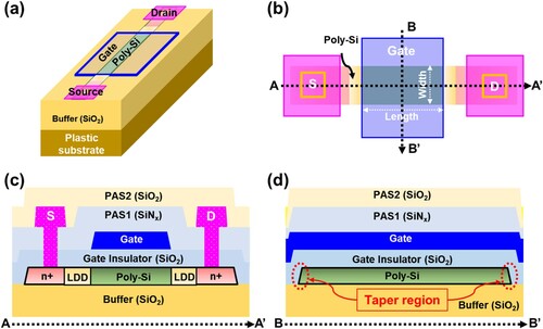
Table 1. Conditions for CED Process in LTPS TFTs
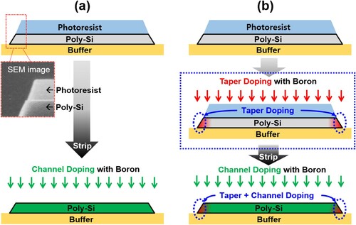
The comparison between the conventional channel doping and CED processes is shown in Figure . In the conventional channel doping process, ion implantation with boron is usually performed after the removal of the photoresist, as illustrated in Figure (a). In addition to the steps followed in the conventional channel doping process, the CED process involves an additional channel doping step, which is defined as taper doping (Figure [b]). In the CED process, the first boron implantation is performed before the photoresist is removed, followed by a second boron implantation step after its removal. Consequently, the CED process results in a higher level of doping in the taper region than in the main channel region, while the conventional channel doping results in equal concentration of boron in the entire channel region. The conditions for the CED process are presented in Table .
Figure 2. Comparison between the (a) conventional channel doping and (b) channel edge doping (CED) process.
The transfer curves of the LTPS TFTs fabricated by the conventional channel doping and the CED process were measured in the dark at room temperature using a B1500A semiconductor device parameter analyzer. During the measurements, the gate voltage (VGS) was swept from −5 to +10 V, while the drain voltage (VDS) was fixed at 0.1 and 10 V, and the source electrode was grounded.
3. Results and discussion
3.1. Measured hump characteristic
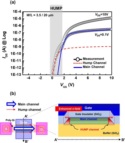
Figure (a) illustrates the transfer characteristics with the threshold voltage (VTH) of 2.2 V measured at VDS = 0.1 and 10 V in LTPS TFTs with the conventional channel doping process. The hump phenomenon, which leads to anomalous current, was observed in the sub-threshold regime at VGS = 0–2 V of the transfer curve. As mentioned above, previous studies have explained that the hump characteristic is caused by the hump channel in the taper region, as indicated in Figure (b) [Citation10–12]. When the VTH of the additional hump channel is lower than that of the main channel, the current starts to flow through the hump channel earlier than the main channel as the gate voltage increases, and later flows through the main channel, eventually resulting in hump-shaped current curves. In this respect, the measured results can be explained by the transfer curve at VDS = 0.1 V consisting of two current paths: the main channel with a VTH of 2.2 V denoted by a blue solid line, and the hump channel with a VTH of 0.7 V denoted by a red dotted line. In order to reduce the hump phenomenon, it is recommended that a CED technique is used to eliminate the hump channel, which is the main cause of the hump phenomenon.
Figure 3. (a) Measured transfer curve with hump characteristics at VDS = 0.1 and 10 V in LTPS TFTs with the conventional channel doping process, and (b) schematic illustration of the hump channel and main channel in the sub-threshold regime at VGS < VTH.
3.2. Numerical analysis of hump phenomena
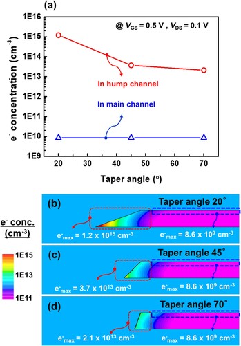
In order to analyze the hump mechanism, physical parameters, such as the e-field and electron (e−) concentration distribution, were investigated from the cross-sectional view in the width direction along a one-dimensional (1D) cut-line (A’ to B’) from the results of the TCAD simulation, as shown in Figure 4.2. The e-field was enhanced at the channel edge region at VGS = 1 V in the sub-threshold regime with hump characteristics (Figure [b]). Thus, electrons were crowded into the channel edge region much more than the main channel (Figure [c]). In contrast, at VGS = 3 V, which is higher than VTH ( = 2.2 V), the electron concentration of the main channel increased from ∼1010 cm−3 to ∼1016 cm−3 (Figure [d]) [Citation14]. This indicates that the hump characteristics are attributed to the hump channel generated from the crowded electrons by a strong e-field at the channel edge at low VGS in the sub-threshold regime before the main channel turns on. Figure shows the variation in electron concentration at the hump channel with taper angles of 20°, 45°, and 70° in the sub-threshold regime at VGS = 0.5 V and VDS = 0.1 V. The electron concentration in the hump channel decreases as the taper angle increases. Meanwhile, the electron concentration in the main channel is not affected by the taper angle. This result indicates that the hump characteristics are extremely sensitive to the shape of the channel edge of the LTPS TFTs. However, the hump characteristics have been improved by changing the specific shape of the tapered region in the previous studies [Citation10,Citation11]. These hump-reduction methods may cause the non-uniform luminance issue over the entire panel area due to the variation in the shape at the taper region caused by the complex fabrication process. Therefore, to improve the hump characteristics, it is necessary to either reduce the e-field or control the electron concentration at the channel edge region. We focused on controlling the electron concentration selectively at the channel edge region by using a channel doping process. Our CED process is a technique for controlling electron concentration only at the channel edge region.
Figure 4. Simulated physical properties along a 1D cut-line (A’ to B’) of (a) the 3D simulation structure for LTPS TFTs at VDS = 0.1 V, (b) the e-field distribution at VGS = 1, and the electron concentration distribution within the active layer at VGS = (c) 1 V and (d) 3 V.
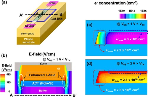
Figure 5. (a) Electron concentration according to taper angle, and simulated electron concentration distributions at taper angles of (b) 20°, (c) 45°, and (d) 70° at VGS = 0.5 V.
3.3. Channel edge doping (CED) effect for hump reduction
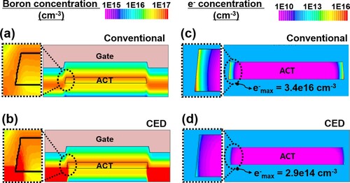
Figure displays the comparison between the simulation results obtained for the conventional channel doping and CED processes at VGS = 1 V and VDS = 0.1 V in sub-threshold regime. When the CED is performed, a higher level of doping is observed in the taper region as compared to the conventional channel doping process (Figures [a] and 6[b]). In the n-type LTPS TFTs, boron acted as an acceptor and decreased carrier concentration [Citation15]. The simulation results indicate that heavily doped boron at the taper region reduces the number of electron carriers, thus resulting in a decrease in the e−max from 3.4 × 10¹⁶ to 2.9 × 1014 cm−3 compared to the conventional channel doping (Figures [c] and 6[d]).
Figure 6. Comparison of simulation results between the different channel doping methods at VGS = 1 V and VDS = 0.1 V: Boron concentration with (a) conventional and (b) CED process, and electron concentration within an active layer with (c) conventional and (d) CED process.
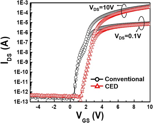
Based on the simulation results, we conclude that the channel edge effect can be effectively eliminated by employing the CED technique. In order to verify whether this is the case, we fabricated LTPS TFTs by using the CED process with the doping conditions used in the simulation. Figure demonstrates the results of our measurements of the LTPS TFTs fabricated by the conventional doping and CED process. The hump phenomenon is not observed in the transfer curve of the samples fabricated by the CED process, while the hump-shaped transfer curves are observed in the samples where the conventional doping process was employed. Consequently, we conclude that the CED process leads to an effective reduction in the hump characteristics, given the excellent agreement between the simulation and experimental results.
Figure 7. Measured transfer curves at VDS = 0.1 and 10 V in LTPS TFTs with conventional channel doping and CED process.
4. Conclusion
In this study, we proposed that the CED process can be used to reduce the hump characteristics that limit the performance of the n-type LTPS TFTs. Through the CED process, robust LTPS TFTs were fabricated and their transfer curves do not exhibit the hump phenomenon. Additional boron is doped selectively at the taper region during the CED process, thus enabling control over the carrier concentration in the taper area. Comparative analysis of the devices fabricated by the conventional channel doping and the CED processes was performed via TCAD simulation and experimental measurements. The CED technique does not require the use of additional masks and is easy to implement as compared to the conventional solutions for hump issues, such as changing the taper shapes. The results obtained from our study would be extremely useful for fabricating high-performance LTPS TFTs for AMOLED displays.
Disclosure statement
No potential conflict of interest was reported by the author(s).
Additional information
Funding
Notes on contributors

Ki Woo Kim
Ki Woo Kim received a Ph.D. degree from the School of Electrical and Electronic Engineering, Yonsei University, Seoul, South Korea, in 2021. He has been researching on panel design and thin-film transistors for AMOLED mobile display applications.

Heesoo Lee
Heesoo Lee received a Ph.D. degree from the School of Electrical and Electronic Engineering, Yonsei University, Seoul, South Korea, in 2019. She has been researching on thin-film transistors based on metal oxide materials.

Hyun Jae Kim
Hyun Jae Kim received a Ph.D. degree from the Department of Materials Science and Engineering, Columbia University, New York City, NY, USA, in 1996. Since 2005, he has been a Professor at the Faculty of the School of Electrical and Electronic Engineering, Yonsei University, Seoul, South Korea.
References
- M. Stewart, R. S. Howell, L. Pires, and M. K. Hatalis, IEEE Trans. Electron Devices. 48 (5), 845–851 (2001).
- T. Suzuki, Appl. Phys. Lett. 99, 111101-1–111101-15 (2006).
- S. H. Na, W. K. Min, D. H. Kim, H. W. Hwang, Y. M. Ha, and H. J. Kim, J. Inf. Disp. 22 (4), 275–284 (2021).
- K. W. Kim, J. Kang, H. Ku, K. Lee, and H. J. Kim, IEEE Electron Device Lett. 39 (10), 1524–1527 (2018).
- H. W. Hwang, S. Hong, S. S. Hwang, K. W. Kim, Y. M. Ha, and H. J. Kim, IEEE Electron Device Lett. 40 (7), 1108–1111 (2019).
- C. –C. Liao, M. –C. Lin, T. –Y. Chiang, and T. –S. Chao, IEEE Trans. Electron Devices. 58 (11), 3812–3819 (2011).
- H–J Chung, D–H Kim, and B–K Kim, J. Inf. Disp 6 (4), 6–10 (2005).
- A. Nathan, G.R. Chaji, and S.J. Ashtiani, J. Disp. Technol. 1 (2), 267–277 (2005).
- W. Liu, G. Yao, C. Jiang, Q. Cui, and X. Guo, J. Disp. Technol. 10 (12), 991–994 (2014).
- A. Valletta, P. Gaucci, L. Mariucci, G. Fortunato, and F. Templier, J. Appl. Phys. 104, 124511-1–124511-6 (2008).
- S.P. Kim, J.Y. Oh, J.Y. Yang, M.S. Yang, and I.J. Chung, ECS Transactions 3 (8), 63–67 (2006).
- P. Sallagoity, M. Ada-Hanifi, M. Paoli, and M. Haond, IEEE Trans. Electron Devices. 43 (11), 1900–1906 (1996).
- X. Gao, L. Lin, Y. Liu, and X. Huang, J. Disp. Technol. 11 (8), 666–669 (2015).
- H. Lee, K.S. Chang, Y.J. Tak, T.S. Jung, J.W. Park, W.-G. Kim, J. Chung, C.B. Jeong, and H.J. Kim, Sci. Rep. 6, 35044 (2016).
- J. Y. W. Seto, J. Appl. Phys. 46 (12), 5247–5254 (1975).