
Abstract
Triplet–triplet fusion (TTF) has been an efficiency-enhancing mechanism in fluorescent organic light-emitting diodes (OLEDs) caused by the collision of two triplet excitons. However, achieving a high TTF ratio in fluorescent OLEDs has been difficult despite device strategies to maximize the triplet exciton density within a narrow recombination zone near the electron blocking layer (EBL) due to charge imbalance and hole accumulation between the TTF type emitter and EBL. Based on a trap-detrap mechanism, we were able to realize an improved TTF ratio and reduce hole accumulation by adding a TTF-assisting material (TTF-AM) in the TTF emitter. The TTF-AM served as the hole transport channel, triggering hole trap and detrap while improving the hole transport character of the emitting layer. Through the process of hole detrapping, the improved hole transport properties balanced carriers and generated more triplet excitons in order to activate the TTF mechanism from low to high current density ranges. By adjusting the TTF-AM, the TTF ratio of the anthracene-based emitter was increased from 5.5/20.1% to 13.4/25.5% (low/high current density), thereby resulting in more than doubled external quantum efficiency at low current density.
Introduction
Blue fluorescent organic light-emitting diodes (OLEDs) are still being recognized as blue devices for commercial applications due to their long-term operation and good color purity. Despite having a high external quantum efficiency (EQE), thermally activated delayed fluorescent (TADF) and phosphorescent OLEDs could not robustly survive during the long-term driving due to the high emission energy and long exciton lifetime of the TADF and phosphorescent emitters.[Citation1–5] Moreover, the relatively poor color purity caused by charge-transfer emission of TADF emitters and vibrational peaks of phosphors is a challenge to their commercialization in deep blue OLEDs. Therefore, it is strongly suggested to further upgrade the EQE and device life span of the blue fluorescent OLEDs until the practical application of the blue TADF or phosphorescent OLEDs.
Currently, triplet–triplet fusion (TTF) type fluorescent OLEDs are widely used as blue devices for high EQE in commercial products. In addition to the pristine singlet excitons generated by the electrical injection of carriers, extra radiative singlet excitons in the TTF mechanism are formed by the collision of two triplet excitons. The amount of extra singlet excitons is determined by the up-conversion efficiency of the triplet excitons, thereby indicating that it is a key factor in the high EQE of the TTF type blue fluorescent OLEDs.[Citation6–11] Therefore, material and device engineering has been attempted in order to enhance the triplet exciton to singlet exciton transformation by TTF process. In order to increase the TTF ratio for high EQE, anthracene moiety has been used as the main building block of the TTF material, and it was modified with various electron donating and withdrawing substituents.[Citation12–14] The TTF ratio increased dramatically by substituting dibenzofuran unit to the anthracene core. Device approaches, such as inserting an efficiency enhancement layer to confine triplet excitons and optimizing the charge balance, were also effective for the high TTF ratio.[Citation15] Despite the importance of the TTF process control, no systematic study managing the TTF mechanism in the emitting layer to achieve high EQE in the TTF blue OLEDs has been carried out. Although several high efficiency TTF devices have been reported, it is uncommon to find an effective method of increasing the TTF ratio.
Here, we suggest a trap-detrap process in the emitting layer to improve the EQE and TTF efficiency of blue OLEDs by introducing a TTF-assisting material (TTF-AM) that facilitates the TTF mechanism. The addition of TTF-AM was described as suppressing hole accumulation between the electron blocking layer (EBL) and the emitting layer, as well as increasing the triplet exciton density in the anthracene-based TTF material. As a result, the EQE of blue OLEDs was improved by increasing the TTF ratio from 5.5/20.1% to 13.4/25.5% at low/high current density. In particular, the TTF-AM more than doubled the EQE at low current density.
Results and discussion
In general, the TTF mechanism originates from the collision of two triplet excitons in the emitter, and it is facilitated by effective triplet exciton formation in a narrow recombination zone. In TTF-type blue fluorescent OLEDs, a narrow recombination zone is formed near the EBL, thus leading to hole accumulation and electron leakage at the interface between the EBL and the TTF emitting layer. As a result, the TTF ratio in conventional TTF devices would be degraded, and the EQE of the devices would be damaged. The management of hole accumulation and TTF ratio is also critical to the EQE of the blue fluorescent OLEDs. A device approach introducing a TTF-AM that manages the hole accumulation and TTF ratio was used as a methodology to increase the TTF ratio. The TTF-AM relies on an appropriate highest occupied molecular orbital (HOMO) level for good hole injection and efficient exciton formation via detrapping. Good hole injection would relieve hole accumulation and improve carrier balance, while efficient hole detrapping would increase triplet exciton density for high TTF ratio. The emission process hiring the TTF-AM is shown in Figure .
Figure 1. The emission process of the conventional TTF device and TTF-AM device.
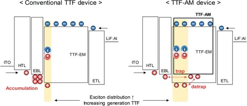
Figure 2. (a) Energy level diagram of devices and chemical structure of materials, (b) Current density-voltage-luminance (J-V-L), (c) External quantum efficiency (EQE)-current density, and (d) EL spectra at 1,000 cd/m2 of the TTF devices.
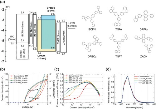
Figure 3. The transient EL measurement from low to high current density range according to the doping concentration of the TTF-AM (10, 20, and 30 wt%) of the conventional TTF and TTF-AM device: (a) 10, (b) 70, (c) 150 current density and EL intensity-1/2-time (inset), and (d) EQE-current density (up) and TTF ratio-current density (down).
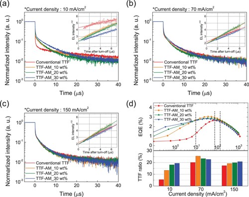
Figure 4. The transient EL of the conventional TTF and TTF-AM doped (30 wt% doping) devices at voltage pulses of (a) 1, (b) 10, (c) 50, and (d) 100 µs under a current density of 150 mA/cm2.
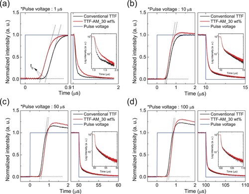
Figure 5. The impedance data of conventional TTF and TTF-AM 30 wt% devices: (a) capacitance-voltage at AC frequency of 50 Hz, 3-D plot of capacitance-frequency-voltage of (b) conventional TTF, and (c) TTF-AM 30 wt% device (light-emitting devices in [a] and hole-only device in [b, c]).
![Figure 5. The impedance data of conventional TTF and TTF-AM 30 wt% devices: (a) capacitance-voltage at AC frequency of 50 Hz, 3-D plot of capacitance-frequency-voltage of (b) conventional TTF, and (c) TTF-AM 30 wt% device (light-emitting devices in [a] and hole-only device in [b, c]).](/cms/asset/47d441e5-204f-478c-b994-8c01776b51fb/tjid_a_2089750_f0005_oc.jpg)
The anthracene-based 2-(10-phenylanthracen-9-yl)dibenzo[b,d]furan (DBFAn) was a TTF-emitting material (TTF-EM) and 7,7'-diphenyl-7H,7'H-10,10'-bibenzo[c]carbazole (DPBCz) was the TTF-AM. The TTF devices were fabricated by doping the TTF-AM (10, 20 and 30 wt%) in the DBFAn. Detailed information about the device structure is shown in the experimental part and Figure (a). In the current density–voltage-luminance (J-V-L) data in Figure (b), the current density of the TTF devices was increased according to the doping concentration of the TTF-AM because of the direct injection of hole carriers into the TTF-AM with a small energy barrier (0.17 eV) for hole injection from the EBL due to the shallow HOMO level of −5.83 eV. Electron injection would not be improved at all because of the large lowest unoccupied molecular orbital (LUMO) barrier (0.50 eV) for electron injection. The HOMO and LUMO energy levels of the TTF-EM and TTF-AM measured by cyclic voltammetry are shown in Figure S2. The experimental part contains the detailed information about the measurement method.
The EQE of the TTF devices in Figure (c) was significantly affected by the carrier injection behavior of the devices. The conventional device without the TTF-AM showed very low EQE at low current density and improved EQE at high current density. Poor hole injection and hole accumulation unbalanced carriers, thereby reducing the EQE of the TTF device. Moreover, low TTF probability resulting from low triplet exciton density at low current density is also responsible for the low EQE. The hole injection is facilitated at a high voltage, which improves the EQE of the TTF device at high current density. High triplet exciton density also contributes to the improved EQE via the TTF mechanism. Due to the high hole density balancing the carriers and high triplet exciton density, the addition of the TTF-AM enhanced the overall EQE current density ranges. More triplet excitons can be generated by the injected hole carriers, thus allowing the TTF mechanism in the DBFAn to be activated. As a result, the maximum EQE was improved from low to high current density ranges when compared with the conventional TTF devices without the TTF-AM. In particular, the EQE of the conventional TTF device was lower than that of the TTF-AM doped devices at low current density because the TTF mechanism was ineffective in the DBFAn material due to the hole accumulated between the EBL and the EML. All TTF devices exhibited the same electroluminescence (EL) spectra regardless of the TTF-AM doping concentration, as shown in Figure (d). All device data are summarized in Table .
Table 1. Summarized device performances of the TTF devices with 10, 20, and 30 wt% TTF-AM.
Transient EL measurement was used to analyze the TTF ratio from low to high current density range according to the doping concentration of TTF-AM (Figure ). In general, the delay component in the transient EL analysis is caused by the TTF process, which converts triplet excitons into singlet excitons. At low current density (10 mA/cm2), the conventional TTF device did not show significant delayed decay after voltage turn-off, whereas the TTF-AM doped TTF devices showed substantial delayed decay derived from TTF mechanism, as shown in Figure (a). The delayed decay of transient EL was largely increased at high current density (70 and 150 mA/cm2) regardless of the TTF-AM doping concentration, as shown in Figure (b) and (c). The TTF ratios of the 0/10/20/30 wt% TTF-AM doped TTF devices based on the TTF ratio equation in the literature were 5.5/13.4/18.1/19.4, 20.1/25.5/23.4/22.7, and 17.4/19.2/19.9/20.8% at 10, 70, and 150 mA/cm2, respectively, as shown in Figure (d).[Citation16–18] Supporting information contains detailed data on the TTF ratio calculation. The TTF ratio varies with the current density, and it is well correlated with the EQE of the devices. The EQE was increased according to the TTF-AM content at 10 mA/cm2, which corresponded with the TTF ratio of the TTF devices. The EQE at high current density also followed the trend of the TTF ratio. However, the EQE at 150 mA/cm2 was not well correlated with the TTF ratio due to the exciton quenching processes such as singlet–triplet annihilation and singlet-polaron annihilation at high exciton and polaron density. The TTF device with 10% TTF-AM recorded the highest EQE and highest TTF ratio at the same time. As a result, the TTF-AM increased the TTF ratio by suppressing hole accumulation via improved hole injection.
In order to analyze the hole accumulation between EBL and EML, the pulse interval of transient EL was changed as 1, 10, 50, and 100 µs under a high current density of 150 mA/cm2, as shown in Figure . High current density was used in order to accurately analyze hole accumulation via transient EL over a wide pulse interval. The conventional TTF device and the TTF device with 30 wt% TTF-AM were compared. Since carrier behavior depends on voltage pulse duration time even at high current density, controlling the voltage pulse width from 1 to 100 µs can trace the hole accumulation and carrier recombination. This is confirmed by the onset time of the transient EL (t0), which corresponds to the time for recombination by capturing electrons and holes.[Citation19, Citation20] The TTF-AM doped device showed a shorter t0 of 0.32/0.45 µs than 0.43/0.51 µs of the conventional TTF device at a voltage pulse of 1/10 µs, as shown in Figure (a) and (b). It was also confirmed that more delay components are formed after the turn-off. TTF-AM doping suppressed hole accumulation through efficient hole injection, thereby inducing a trap-detrap mechanism between TTF-AM and TTF-EM. This resulted in quick recombination and more delay components by TTF. However, the increase of the voltage pulse to 50 and 100 µs slowed the recombination of the TTF-AM doped device considering the larger t0 of 0.60 and 0.63 µs of the TTF-AM doped device than 0.51 and 0.54 µs of the TTF-AM free device, respectively, as shown in Figure (c) and (d). Hole injection and recombination were efficient even in the TTF-AM device under long voltage pulse. The exciton formation mechanism of the TTF-AM doped device was relatively slowed due to the trap-detrap process, thereby impeding the recombination. As a result, the increase of delayed component by the TTF-AM was not dramatic, as the accumulation of the holes between EBL and EML is not significant. Furthermore, it was found that the normalized light intensity of the TTF-AM doped devices in the turn-on time range is higher than that of the conventional device at all pulse voltages (1, 10, 50, and 100 µs). The remaining carriers without recombination can be interpreted as being merged with the newly injected carriers from the next cycle of turn-on voltage pulse.[Citation21] Therefore, it was confirmed that the TTF-AM doping suppressed hole accumulation, while increasing exciton formation and delay component via trap-detrap mechanism.
Impedance analysis was used to investigate intrinsic carrier behavior through the capacitance–voltage (C-V) and capacitance-frequency (C-F) measurements in order to further study the trap-detrap process between TTF-AM and TTF-EM. The C-V relationship of the device was analyzed by comparing the TTF-AM doped (30 wt%) device and TTF-AM free device (conventional TTF device), as shown in Figure (a).[Citation22–25] A schematic diagram was presented in order to show the hole carrier behavior in the device. For the device analysis, alternating current (AC) at a frequency of 50 Hz was applied. A geometric capacitance value of 1 nF was observed at a low voltage (0∼1.0 V, region I). In addition, the capacitance value was slightly increased by hole accumulation between the hole transport layer (HTL, BCFN) and EBL (TNPA) in region II (1.0∼1.8 V) both in the conventional TTF and TTF-AM doped devices. The capacitance in region III (1.8∼2.3 V) of the TTF-AM free device was sharply increased due to hole accumulation between EBL and TTF-EM, whereas it was slightly increased in the TTF-AM doped device due to a slight hole accumulation by efficient hole injection from EBL to TTF-AM. The increase in capacitance of the TTF-AM doped device was significant in region IV (2.3∼2.9 V) via detrapping of holes from TTF-AM to TTF-EM. The recombination of carriers reduced the capacitance after reaching maximum capacitance because the recombination rate is higher than the carrier accumulation rate.[Citation26–28] Since electrical traps did not exist in the EML, the increase in capacitance was attributed to charge accumulation in the conventional TTF device. Meanwhile, the trap-detrap process caused the phase shift of the capacitance.
C-F measurement was used to analyze the behavior of the carrier. The TTF and TTF-AM doped hole-only devices were characterized at various operating voltages by varying the frequency from 100 Hz to 10,000 Hz. The 3D plots of C-V and C-F of the hole-only devices are shown in Figure (b) and (c). In the C-F relationship, the conventional TTF device showed similar capacitance values across all frequency ranges, thereby indicating that only charge accumulation contributed to the increase of the capacitance. In contrast, the TTF-AM (30 wt%) doped device exhibited a gradual increase in capacitance with decreasing frequency due to the trap-detrap process via TTF-AM in the EML. The detrap process was suppressed at high frequency because the transit time of the specific trap state was shorter than that of the oscillating voltage, thus resulting in low capacitance.[Citation29] Regardless of voltage or frequency, the capacitance was kept constant at a low voltage prior to the hole injection into the EML. Both DC and AC analysis via current density–voltage and impedance measurements supported that performance enhancement via TTF-AM was derived from efficient charge transport from EBL to EML resulting from a lowered energetic barrier and the charge storage effect of TTF-AM. The C-F relationship of the TTF-AM doped (0, 10, 20, and 30 wt%) is presented in Figure S3. They showed a gradual increase in the capacitance due to the activated trap-detrap process via TTF-AM. Furthermore, light-emitting devices were used to investigate the C-F of conventional TTF and TTF-AM (30 wt%) doped devices, as shown in Figure S4. They showed a similar tendency as increased capacitance through the trap-detrap process of the hole-only device. The TTF-AM could generate the trap-detrap process and improve the TTF ratio and EQE.
Conclusion
A TTF-AM device that stimulates the TTF mechanism through a trap-detrap mechanism was developed, and it effectively improved the EQE of the TTF device. The TTF-AM served as the hole transport channel triggering hole trap and detrap while improving the hole transport character of the emitting layer. The improved hole transport properties balanced carriers and generated more triplet excitons in order to activate the TTF mechanism through the hole detrapping process from low to high current density ranges. The TTF ratio of the anthracene-based emitter was enhanced from 5.5/20.1% to 13.4/25.5% (low/high current density) by adjusting the TTF-AM, thereby resulting in more than doubled EQE at low current density. Therefore, the device concept of this work may contribute to enhancing the EQE of the TTF devices.
Experimental
Generation information
The HOMO and LUMO energy levels were measured in dilute solution using cyclic voltammetry (Ivium Tech., Iviumstat) from the onset point of the first peak of oxidation and reduction potential. Ferrocene served as the standard material, 0.1 M tetrabutylammonium perchlorate in acetonitrile served as the electrolyte, carbon tube served as a working electrode, Pt wire served as a counter electrode, and Ag/AgCl served as a reference electrode.
Device fabrication and measurements
Full devices were fabricated by using the stack structure of indium tin oxide (ITO, 50 nm)/BCFN:HATCN (40 nm:30 wt%)/BCFN (10 nm)/TNPA (10 nm)/DPFAn:DPBCz (30 nm:X wt%)/TNPT (5 nm)/ZADN (20 nm)/LiF (1.5 nm)/Al (200 nm). Single-carrier devices were fabricated by using the device structure of ITO (50 nm)/BCFN:HATCN (40 nm:30 wt%)/BCFN (10 nm)/TNPA (10 nm)/DPFAn:DPBCz (30 nm:X wt%)/DNTPD (10 nm)/Al (200 nm), where BCFN is N-([1,1'-biphenyl]−4-yl)−9,9-dimethyl-N-(4-(9-phenyl-9H-carbazol-3-yl)phenyl)−9H-fluoren-2-amine, TNPA is tris(4-(naphthalen-1-yl)phenyl)amine, TNPT is 2,4,6-tris(4-(naphthalen-1-yl)phenyl)−1,3,5-triazine, ZADN is 2-[4-(9,10-di-naphthalen-2-yl-anthracen-2-yl)-phenyl]−1-phenyl-1H-benzoimidazole, and LiF is lithium fluoride. Evaporation was used to deposit all layers, and the final test coupons were encapsulated by a glass lid for the device test. The device performance was measured by using a Keithley 2400 and the CS 2000 (Konica Minolta Inc.) spectroradiometer.
The transient EL measurement was performed by using a function generator (Keysight 33622A), an oscilloscope (Yokogawa DL9140) with photomultiplier tube (HAMAMATSU G1760001), and a current amplifier (DHPCA-100). The impedance analysis was carried out by using the Zurich Instruments MFIA 5 MHz Impedance Analyzer.
Disclosure statement
No potential conflict of interest was reported by the author(s).
Additional information
Notes on contributors

Kyung Hyung Lee
Kyung Hyung Lee received his B.S. degree from the Department of Information Display, Hoseo University, Korea. He is currently pursuing an M.S.-Ph.D. integrated course at the School of Chemical Engineering of Sungkyunkwan University. His research interest areas include the development of exciton dynamics, degradation mechanism, and emission mechanism for organic light-emitting diodes.

Jae Min Kim
Jae-Min Kim received his B.S. degree from the Department of Materials Science and Engineering, Seoul National University, Korea. He obtained a Ph.D. from the Department of Materials Science and Engineering, Seoul National University, Korea under the supervision of Professor Jang-Joo Kim. After graduation, he joined Samsung Display as a staff engineer and performed cutting-edge research on the high performance of organic light-emitting diodes for the Galaxy and iPhone series. He is currently a postdoctoral fellow at Sungkyunkwan University, Korea. His research interests include exciton and polaron dynamics, degradation mechanism, and machine learning-aided materials/devices design in organic light-emitting diodes.

Sook-Hee Jeong
Sookhee Jeong received her Ph.D. degree in chemical engineering at Sungkyunkwan University, Korea. She works as an organic electronic materials researcher and develops a novel device structure for organic electronics devices. Her main areas of research include the synthesis of blue phosphorescent organic electronic host materials and synthesis of blue TADF materials.

Ji Ho Baek
Baek Ji Ho received his Ph.D. degree from Hanyang University, Korea in 2015, and he joined LG.Philips LCD (LG Display) and developed LCD materials and p-OLED for 22 years. Following that, he worked as the Head of OLED Technology. He has been the Vice President of LG Display since 2020.

Jeong Dae Seo
Jeong Dae Seo has been working for LG Display for 22 years, developing active matrix organic light-emitting diodes. He is currently a senior researcher engineer at LG Display.

Inbum Song
In Bum Song has been working for LG Display for 15 years, developing active matrix organic light-emitting diodes. He is currently a senior researcher engineer at LG Display.

Sang Beom Kim
Sang Beom Kim has been working for LG Display for 6 years, developing active matrix organic light emitting diodes. He is currently a senior researcher engineer at LG Display.

Hyun Chul Choi
Hyun Chul Choi received his Ph.D. degree from Korea Advanced Institute of Science and Technology, Korea in 1994. He worked for LG Electronics (LG.Philips LCD) and developed LCD panels for 21 years. Following that, he worked as the Head of OLED Technology. He has been working as the Senior Vice President of LG Display since 2021.

Jun Yeob Lee
Jun Yeob Lee received his Ph.D. degree from Seoul National University, Korea in 1998. After his postdoctoral research fellowship at Rensselaer Polytechnic Institute (1998∼1999), he joined Samsung SDI and developed active matrix organic light-emitting diode for 6 years. Following that, he worked as a professor at the Department of Polymer Science and Engineering of Dankook University. He has been working as a professor at the School of Chemical Engineering of Sungkyunkwan University since 2015. His main research areas include the synthesis of organic electronic materials and development of novel device structure for organic electronic devices.
References
- M.A. Baldo, D.F. O'Brien, Y. You, A. Shoustikov, S. Sibley, M.E. Thompson, and S.R. Forrest, Nature 395, 151 (1998).
- C.Y. Chan, M. Tanaka, Y.T. Lee, Y.W. Wong, H. Nakanotani, T. Hatakeyama, and C. Adachi, Nat. Photonics, 15, 203 (2021).
- S.O. Jeon, K.H. Lee, J.S. Kim, S.G. Ihn, Y.S. Chung, J.W. Kim, H. Lee, S. Kim, H. Choi, and J.Y. Lee, Nat. Photonics 15, 208 (2021).
- M. Jung, K.H. Lee, J.Y. Lee, and T. Kim, Mater Horizons 7, 559 (2020).
- H. Uoyama, K. Goushi, K. Shizu, H. Nomura, and C. Adachi, Nature 492, 234 (2012).
- D.W. Di, L. Yang, J.M. Richter, L. Meraldi, R.M. Altamimi, A.Y. Alyamani, D. Credgington, K.P. Musselman, J.L. MacManus-Driscoll, and R.H. Friend, Adv. Mater 29, 1605987 (2017).
- R. Ieuji, K. Goushi, and C. Adachi, Nat Commun, 10, 5283 (2019).
- S.K. Kim, B. Yang, Y. Ma, J.H. Lee, and J.W. Park, J. Mater. Chem 18, 3376 (2008).
- D.Y. Kondakov, J. Appl. Phys 102, 114504 (2007).
- D.Y. Kondakov, T.D. Pawlik, T.K. Hatwar, and J.P. Spindler, J. Appl. Phys 106, 124510 (2009).
- Y.J. Pu, G. Nakata, F. Satoh, H. Sasabe, D. Yokoyama, and J. Kido, Adv. Mater 24, 1765 (2012).
- C.H. Chien, C.K. Chen, F.M. Hsu, C.F. Shu, P.T. Chou, and C.H. Lai, Adv. Funct. Mater 19, 560 (2009).
- Y.H. Kim, H.C. Jeong, S.H. Kim, K.Y. Yang, and S.K. Kwon, Adv. Funct. Mater 15, 1799 (2005).
- P.I. Shih, C.Y. Chuang, C.H. Chien, E.W.G. Diau, and C.F. Shu, Adv. Funct. Mater 17, 3141 (2007).
- H. Lim, H.J. Cheon, G.S. Lee, M. Kim, Y.H. Kim, and J.J. Kim, ACS Appl. Mater. Interfaces 11, 48121 (2019).
- S. Kang, J.Y. Lee, and T. Kim, Electron. Mater. Lett 16, 1 (2020).
- H. Kuma, and C. Hosokawa, Sci. Technol. Adv. Mater 15, 034201 (2014).
- B.H. Wallikewitz, D. Kabra, S. Gelinas, and R.H. Friend, Phys Rev B 85, 045209 (2012).
- S. Barth, P. Muller, H. Riel, P.F. Seidler, W. Riess, H. Vestweber, and H. Bassler, J Appl Phys 89, 3711 (2001).
- J.Y. Kang, J.B. Son, G.W. Kim, S. Bae, K.S. Min, S. Sul, W.S. Jeon, J. Jang, G.S. Park, J.K. Shin, J.H. Kwon, and S.K. Kim, Phys. Status Solidi A 217, 2000081 (2020).
- J.H. Lee, S. Lee, S.J. Yoo, K.H. Kim, and J.J. Kim, Adv. Funct. Mater 24, 4681 (2014).
- L. Burtone, J. Fischer, K. Leo, and M. Riede, Phys. Rev. B 87, 045432 (2013).
- L. Burtone, D. Ray, K. Leo, and M. Riede, J. Appl. Phys 111, 064503 (2012).
- J.M. Kim, and J.J. Kim, Org Electron 67, 43 (2019).
- C. Weichsel, L. Burtone, S. Reineke, S.I. Hintschich, M.C. Gather, K. Leo, and B. Lussem, Phys. Rev. B 86, 075204 (2012).
- S. Nowy, W. Ren, A. Elschner, W. Lovenich, and W. Brutting, J. Appl. Phys 107, 054501 (2010).
- M. Takada, T. Mayumi, T. Nagase, T. Kobayashi, and H. Naito, Appl. Phys. Lett 114, 123301 (2019).
- L. Zhang, H. Nakanotani, and C. Adachi, Appl. Phys. Lett 103, 093301 (2013).
- M. Weis, T. Otsuka, D. Taguchi, T. Manaka, and M. Iwamoto, J. Appl. Phys 117, 155503 (2015).