
 ?Mathematical formulae have been encoded as MathML and are displayed in this HTML version using MathJax in order to improve their display. Uncheck the box to turn MathJax off. This feature requires Javascript. Click on a formula to zoom.
ABSTRACT
Light field 3D display has attracted great attention as the hardware interface for a virtual 3D application. The design and fabrication of light-modulating structures directly affect the authenticity of the reconstructed 3D image. The critical challenges in 3D display, such as visual fatigue, limited motion parallax, and insufficient light efficiency, are closely related to the inaccurate phase or angular reconstruction of the virtual light field. While the designs of light field modulators are widely introduced in all kinds of studies, the importance of fabrication for 3D display is usually under-estimated. Large format, small feature size, and high precision in shape are the three critical requirements of fabrication for 3D display. In this paper, we focus on the fabrication technologies for light-modulating structures. Fabrication tools for both microstructures and nanostructures are introduced. The fabrication capability, critical challenges and its applications in light field 3D display are discussed. Finally, the future development of 3D display related fabrication technologies are highlighted.
1. Introduction for light field 3D display
With the advent of a 3D world, people have become dissatisfied by the visual perception of 2D imagery. Creating a virtual 3D universe has been man’s dream for 150 years since C. Wheatstone first invented stereoscopy [Citation1]. A virtual 3D image can be reconstructed by discretizing a continuously distributed light field and creating multiple views based on either ray-tracing method or wavefront approach. The term ‘light field' used here either refers to the light ray collection of a 3D scene from the perspective of geometric optics or to the amplitude and phase information of a wavefront in wave optics. With properly arranged views, 3D images with motion parallax and stereo parallax can be visualized by integrating an optical element with a flat panel. Different from other technologies including holographic display and volumetric display, light field 3D display has a compact form factor compatible with portable electronic devices. The function of the optical element in a light field 3D display is to modulate the phase information of light field and generate a finite number of views, while the display panel refreshes the amplitude information. Notably, the modulated phase information of a view in diffractive optics-based 3D display not only refers to the angular deflection, but also includes light intensity distribution, angular separation, and view shape. As illustrated in Figure , parallax barriers, lenticular lens arrays, microlens array, directional backlight, multi-layer LCDs and diffractive optical elements (e.g. diffractive gratings, metasurfaces, etc) have been extensively studied for creating multiple views.
Figure 1. Several approaches of light field reconstruction display. (a) Parallax barrier-based 3D display. (b) Cylindrical lens array-based 3D display. (c) MLA-based 3D display. (d) Spatio-temporal multiplexing-based 3D display. (e) Multi-layer LCD-based 3D display. (f) Diffractive optics-based 3D display. (f) Reproduced with permission [Citation2]. Copyright 2022, Optica Publishing Group.
![Figure 1. Several approaches of light field reconstruction display. (a) Parallax barrier-based 3D display. (b) Cylindrical lens array-based 3D display. (c) MLA-based 3D display. (d) Spatio-temporal multiplexing-based 3D display. (e) Multi-layer LCD-based 3D display. (f) Diffractive optics-based 3D display. (f) Reproduced with permission [Citation2]. Copyright 2022, Optica Publishing Group.](/cms/asset/938bc9af-f891-4c77-ad06-e559ccd7a66b/tjid_a_2118182_f0001_oc.jpg)
Parallax barrier-based 3D display was first developed by F. E. Ives in 1902 [Citation3]. A shaded screen was adopted in front of a screen to orient the emitted light and create parallax, as shown in Figure (a) [Citation4]. Although the parallax barrier has been applied to 3D display owing to its advantages of easily accessible fabrication and low cost, low light efficiency hinders its further development. Cylindrical lens-based 3D display was then employed, as shown in Figure (b), to improve the light efficiency. Similar to the parallax barrier-based 3D display, the direction of light is modulated by the cylindrical lens, forming multiple views in space (Figure (b)). Based on binocular disparity, the 3D images can be formed in the human brain. Despite the limited motion parallax provided by cylindrical lens, it is the technology that is closest to the industrial sector. Most recently, Huang et al. used a head tracking system to expand the FOV to 56.5°, as shown in Figure (c) [Citation5].
Figure 2. (a) Schematic of parallax barrier-based 3D display. Reproduced with permission [Citation4]. Copyright 2015, Optica Publishing Group. (b) Schematic of cylindrical lens array-based 3D display. (c) Images from different perspectives. Reproduced with permission [Citation5]. Copyright 2019, Optica Publishing Group. (d) MLA-based light field 3D display system and corrected elemental image. (e) 3D light-field display results of a 3D image. Reproduced with permission [Citation18]. Copyright 2018, Optica Publishing Group.
![Figure 2. (a) Schematic of parallax barrier-based 3D display. Reproduced with permission [Citation4]. Copyright 2015, Optica Publishing Group. (b) Schematic of cylindrical lens array-based 3D display. (c) Images from different perspectives. Reproduced with permission [Citation5]. Copyright 2019, Optica Publishing Group. (d) MLA-based light field 3D display system and corrected elemental image. (e) 3D light-field display results of a 3D image. Reproduced with permission [Citation18]. Copyright 2018, Optica Publishing Group.](/cms/asset/141b109f-cd44-4335-8c9d-c9eab39d2dae/tjid_a_2118182_f0002_oc.jpg)
Cylindrical lens-based 3D display only provides horizontal parallax, while light field display based on microlens array (MLA) produces full parallax. First proposed by G. Lippmann in 1908 [Citation6], the MLA-based 3D display is realized by recording and reproducing the light field from 3D objects [Citation7–12], based on the optical reversibility theorem (Figure (d)). In recent studies, various novel optical elements [Citation13–15], such as quarter-overlapped MLAs (QOMLA) [Citation16], have been introduced to improve display performance. For example, a bionic compound eye structure was proposed to obtain an FOV of 28° and 22° in the horizontal direction and vertical direction, respectively [Citation17]. A holographic functional screen is used with lens-array to spread beam and recompose the light distribution [Citation18], as shown in Figure (e). MLA is further adopted in near-eye displays to solve vergence and accommodation conflict [Citation19].
Spatio-temporal multiplexing-based 3D display employs a directional backlight and a high-speed liquid crystal display (LCD) panel to achieve full-resolution 3D parallax [Citation20–22]. In spatio-temporal multiplexing-based 3D display, the perspective images are projected to the left and right eyes consecutively through a high-speed LCD in a time-multiplexing manner (Figure (d)). Initially, spatio-temporal multiplexing 3D display is limited to a single user. To solve this problem, an inverted trapezoidal microstructure was designed to split each view into three views for multi-user application [Citation23]. Aside from surface-relief structures, volume-holographic optical elements (VHOEs) were proposed to control the direction of light at a time-multiplexed manner [Citation24]. The schematics of the system are shown in Figure (a).
Figure 3. (a) Schematic of the spatio-temporal multiplexing-based 3D display for multi-users. (b) Schematic of the VHOE-based time-sequential 3D display (c) Demonstrated photographs from the left and right eyes. Reproduced with permission [Citation24]. Copyright 2014, Optica Publishing Group.
![Figure 3. (a) Schematic of the spatio-temporal multiplexing-based 3D display for multi-users. (b) Schematic of the VHOE-based time-sequential 3D display (c) Demonstrated photographs from the left and right eyes. Reproduced with permission [Citation24]. Copyright 2014, Optica Publishing Group.](/cms/asset/63071646-9cdd-40cb-9092-4fdfb7d56e2f/tjid_a_2118182_f0003_oc.jpg)
In multi-layer LCD-based 3D display, or so called ‘tensor display,' stacked liquid crystal (LC) panels are implemented as attenuating layers to define the emitting angle of light beam from the 3D screen, as shown in Figure (e) [Citation25]. In another light-efficient design, a stack of LCDs is sandwiched between a single pair of crossed linear polarizers. The LCDs function as polarization rotators, instead of light attenuators. In a dynamic prototype, an FOV of 10° and views of 7 × 7 [Citation26] were achieved. Optimization algorithms were further developed to improve the optical performance of a tensor display [Citation27,Citation28].
Diffractive optics provide a new approach to reconstructing the light field at a wide viewing angle. Fattal et al. [Citation29] proposed a periodic nanogratings-based 3D display with an FOV of 90°and views of 64. The work paves the way for research on 3D display based on diffractive optical waveguides. To increase the light efficiency and expand the viewing angle, multilevel diffractive optics was subsequently introduced [Citation30–33]. Metalenses, which benefit from their excellent light field modulation capabilities, were used to correct chromatic aberrations in images at an ultra-thin form factor [Citation34]. 1D metagrating with varied spatial frequency and orientation is also adopted as light field modulator to manipulate the angular deflection pixel by pixel. As a result, the angular separation and view arrangement can be freely tailored. Later on, 2D metagrating matrix was adopted in 3D display to reduce crosstalk, increase viewing angle, and manipulate the view distribution [Citation31,Citation35–41].
3D display is the art of light modulation using structures. The design and fabrication of light field modulators directly affect the authenticity of the reconstructed 3D image. Critical challenges, such as visual fatigue, limited motion parallax, insufficient light efficiency, are closely related to the inaccurate phase (or angular) reconstruction of the virtual light field. While designs of light field modulators are widely introduced in all kinds of studies, the importance of fabrication for 3D display is usually under-estimated. In this paper, we focus on the fabrication technologies for light field modulator. The patterning of light field modulator for 3D display clearly falls into the category of extreme fabrication. Firstly, a functional 3D display is in the format of 6–100 inch [Citation33,Citation41,Citation42]. The minimum feature size is in the range of 100 nm–10 mm [Citation18,Citation29,Citation43]. Secondly, to precisely reconstruct the phase information of light field, the tuning capability of surface profile or periodic arrangement of structures is required ideally below 1 nm for precise angular modulation. Therefore, large format, small feature size, and high precision in profiling are the three critical requirements of light field modulator fabrication. Benefiting from the fast growth of fabrication technology, there are several tools that fit the fabrication of structures depending on the scale. For example, MLA is usually fabricated by screening printing [Citation44,Citation45], thermal reflow technology [Citation46–50], ultra-precision machining [Citation51,Citation52], and laser direct writing (LDW). Electron beam lithography (EBL), interferential lithography, and two-photon polymerization lithography (TPL) are widely used to fabricate nanostructures-based light field modulator. In Table , the characteristics of several light field modulators are listed. Geometric optics-based light field modulators have a larger typical structural size, ranging from tens of microns to a few millimeters. In comparison, diffractive optics-based light field modulators offer a larger viewing angle, with smaller typical feature size. In Sections 2 and 3, we highlight multiple fabrication methods and their capability range. Finally, prospects, challenges, and future directions are addressed in Section 4.
Table 1. Characteristics of light field modulators in light field 3D display.
2. Fabrication technology for microstructures and above
2.1. Ultraprecision machining methods
Ultraprecision machining technologies, such as diamond micro-milling and single-point diamond turning (SPDT), are effective methods of fabricating geometric optical elements, including cylindrical lens array and MLA [Citation42,Citation59–66]. All-ending milling usually utilizes single crystal diamond tools to remove metallic materials or polymers [Citation60,Citation67]. After the patterning process, the structured sheet is stripped off and inserted into an injection mold. The geometric optical elements are then mass produced by injection molding process. Based on this method, the surface roughness is less than 10 nm and the peak-to-valley (PV-value) is less than 0.150 µm [Citation68]. Figure (a) shows an MLA processed by a lathe. Although diamond micro-milling has been shown to be an effective fabrication method, inhomogeneity still exists on the turning surface. The most critical issue related to inhomogeneity is the induced vibration of the servo motion in the turning process, which is caused by the inevitable non-smooth trajectory during fabrication [Citation69,Citation70]. To suppress the vibration induced by non-smooth motion, one potential solution is to slow down the moving velocity, which in turn may lead to extremely low machining efficiency. A quasi-elliptical tool servo (QETS) diamond turning technique was proposed by properly decomposing the non-smooth servo motion into two quasi-harmonic smooth motions. The QETS provides the capability to eliminate undesired motion vibrations without reducing the cutting efficiency [Citation71]. Mechanical machining is capable of fabricating cylindrical lens and MLAs with precisely controlled surface profiling. Therefore, aberrations in 3D display can be effectively suppressed, especially at a large viewing angle [Citation72]. Benefiting from the precision profiling capability of diamond turning process, a freeform multi-focal MLA is fabricated to extend the depth of field in 3D display, as shown in Figure (b–e) [Citation52]. Diamond turning is also adopted to fabricate grooved light guide in spatio-temporal multiplexing-based 3D display for separation of views [Citation21]. In addition to fabricating smooth surfaces, ultra-precision machining is also adopted to pattern discontinuous structures, such as Fresnel lens arrays and directional micro grating arrays, by combining the multiple translational and the rotational servo motions [Citation73].
Figure 4. (a) Turning of microlens array on the mental sheet. Reproduced with permission [Citation51]. Copyright 2018, Springer Nature. (b) Schematic of multi- central depth plane 3D display system. (c) Photograph of fabricated MLA. Captured images of virtual 3D targets at different diopters: (d) Focused at 1 diopter, (e) Focused at 1.82 diopter. Reproduced with permission [Citation52]. Copyright 2021, Optica Publishing Group.
![Figure 4. (a) Turning of microlens array on the mental sheet. Reproduced with permission [Citation51]. Copyright 2018, Springer Nature. (b) Schematic of multi- central depth plane 3D display system. (c) Photograph of fabricated MLA. Captured images of virtual 3D targets at different diopters: (d) Focused at 1 diopter, (e) Focused at 1.82 diopter. Reproduced with permission [Citation52]. Copyright 2021, Optica Publishing Group.](/cms/asset/43430044-e760-4e90-b4a5-ab0875e2aa62/tjid_a_2118182_f0004_oc.jpg)
2.2. Inkjet printing and screen printing
Inkjet printing is an additive manufacturing process. Because it is low-cost and easy to operate, the fabrication of MLA has been extensively studied and used [Citation74–77]. In 1994, M. Frlanea et al. [Citation78] proposed a method for preparing MLAs using microjet technology. As shown in Figure (a) [Citation79], droplets are dispensed by a high-frequency microdroplet jetting head. The UV-sensitive resin microdroplets reach the substrate and solidified to form MLA after UV curing. The frequency of injection and the moving speed of the sample platform determine the periodicity of the microlens array, while the volume of droplets and the surface energy of the substrate affects the optical power of MLA. The consistency of surface profiling and positioning accuracy represent a critical challenge in inkjet printing. Y. Peng et al. [Citation80] proposed a fabrication technique of MLAs by combining photolithography with inkjet printing. Hole arrays were prepared by photolithography to define the shape and position of MLA. UV resin droplets were then dispensed into the hole arrays so that a good consistency of geometry parameters was achieved. Despite the simplicity of the preparation process, the technology is usually limited by the viscosity of resin, which in turn limits the refractive index of MLA.
Figure 5. (a) Schematic processes of inkjet printing. Reproduced with permission [Citation79]. Copyright 2011, Optica Publishing Group. (b) Schematic processes of screen printing. (c) 3D perspective images of a microlens. (d) Evolution of NA and radius of MLAs with the reflow time. A photo of 3D reconstruction image viewed from the left 45° direction (e) and right 45° direction (f). Reproduced with permission [Citation81]. Copyright 2011, Springer Nature.
![Figure 5. (a) Schematic processes of inkjet printing. Reproduced with permission [Citation79]. Copyright 2011, Optica Publishing Group. (b) Schematic processes of screen printing. (c) 3D perspective images of a microlens. (d) Evolution of NA and radius of MLAs with the reflow time. A photo of 3D reconstruction image viewed from the left 45° direction (e) and right 45° direction (f). Reproduced with permission [Citation81]. Copyright 2011, Springer Nature.](/cms/asset/2f9e54e7-d563-4648-804d-896951e28abb/tjid_a_2118182_f0005_oc.jpg)
Although multiple jetting head can be adopted to increase the fabrication throughput inkjet printing, screen printing provides a higher fabrication efficiency with the use of a blade or a squeegee to transfer the UV resin onto a substrate. MLA could be obtained after reflow and UV curing. MLAs with diameter ranging from 200 µm to several millimeters were fabricated over large areas at a low cost [Citation44]. Square microlens arrays were also fabricated by adopting a screen with square apertures [Citation57]. Furthermore, the numerical aperture (NA) of the MLA was increased from 0.036 to 0.096 by inverted reflow configuration [Citation81] (Figure (b–f)). Although the geometric parameters of MLAs prepared by inkjet printing and screen printing is controllable to a certain extent by the wettability of the substrate, the dispensed resin volume, and resin viscosity, it is difficult to fabricate freeform optical elements with high precision.
2.3. Thermal reflow technology
Thermal reflow technology, also called photoresist thermal reflow, was proposed by Zoran et al. in 1988 [Citation82]. Photoresist is heated to a molten state and then cooled to form microlenses. The method of fabricating MLAs by photoresist thermal reflow technology utilizes the surface tension of the liquid, i.e. the surface area of the liquid always tends to be minimal (Figure (a,b)) [Citation51]. This method has low equipment requirements, low cost, is simple and easy to implement, and consequently, it is commonly used in the microlens fabrication process [Citation13,Citation46,Citation83–85]. However, several critical challenges exist. First, for the photoresist column with low aspect ratio, a dip will turn up at the center of the lens during thermal reflow process, which makes it very difficult to produce MLA with large F number [Citation84], as shown in Figure (c,d). A thermal reflow method with an additional UV flood exposure and upside down reflow configuration was introduced to eliminate central dip and fabricate MLA with high F number (9.7) [Citation86]. Secondly, although various processing parameters such as the fluidity of photoresist droplets, surface tension and contact angle with the substrate, directly affect the optical power of MLA, the shape precision is relatively low when compared with ultraprecision machining [Citation87]. Extensive studies have been delivered on the influence of substrate wettability and reflow conditions. A contact angle in the range of 2°–76° was obtained [Citation88]. In addition, the filling factor of MLA is limited, because the molten photoresist is prone to fuse during the thermal reflow process when the adjacent photoresist column is too close to each other. The F number, the optical power and filling factors are all important parameters that greatly affect the viewing angle, viewing depth, and stray light in MLA-based 3D display. C. Lin et al. [Citation89] took the lead in melting the hexagonal columnar photoresist structure by thermal reflow, and fabricated a high filling factor honeycomb-arranged hexagonal MLA. In MLA-based 3D display, thermal reflow prepared MLA has been adopted to integrate with pinhole arrays. The proposed system provided an improved image contrast and a MTF50 by up to 32% [Citation90,Citation91], as shown in Figure (e,f).
Figure 6. (a) Schematic processes of thermal reflow technology. Reproduced with permission [Citation51]. Copyright 2018, Springer Nature. (b) SEM image of microlens. (c) Central dips occuring in the microlenses. (d) Profiles of microlenses. (e) MTF curves comparison between the proposed and conventional systems. (f) Light-field image comparison with (top) and without (bottom) MIM-OA. (c) and (d) Reproduced with permission [Citation86], Copyright 2015, RSC Publishing. (b), (e) and (f) Reproduced with permission [Citation91]. Copyright 2021, John Wiley and Sons.
![Figure 6. (a) Schematic processes of thermal reflow technology. Reproduced with permission [Citation51]. Copyright 2018, Springer Nature. (b) SEM image of microlens. (c) Central dips occuring in the microlenses. (d) Profiles of microlenses. (e) MTF curves comparison between the proposed and conventional systems. (f) Light-field image comparison with (top) and without (bottom) MIM-OA. (c) and (d) Reproduced with permission [Citation86], Copyright 2015, RSC Publishing. (b), (e) and (f) Reproduced with permission [Citation91]. Copyright 2021, John Wiley and Sons.](/cms/asset/997173db-7dce-4ff0-a46f-171239560fcc/tjid_a_2118182_f0006_oc.jpg)
2.4. LDW lithography
LDW lithography fabricate microstructures by illuminating photosensitive material using laser beams [Citation92–96]. As a result, the computer-generated image is transferred to a thin layer of photoresist by controlling the dose of exposure through the laser beam. The minimum achievable feature size is a key parameter in the LDW system:
(1)
(1) where λ is the illuminating wavelength; NA is the numerical aperture of the system; and c is a constant determined by the fabrication process and material properties of photoresist. From the equation, lasers with shorter wavelengths contribute to a smaller minimum feature size R [Citation97]. Since the typical value of c is 0.4, the R of LDW system is about half of the wavelength. As a result, the typical R for LDW technique is around 0.5 µm. To improve fabrication throughput, multiple beams were introduced as a parallelization strategy. A 160 µm hexagonal compound eye with a high filling factor (100%), large NA (0.4), ultralow surface roughness (2.5 nm), and aspherical profile was fabricated within 0.85 h [Citation98]. Another parallelization method is based on spatial light modulator (SLM). Instead of writing dot by dot in a single beam LDW system, the SLM-based LDW system fabricates structures frame by frame. Another benefit of the SLM-based LDW is that a wide range of intensity depth can be achieved by SLM. The SLM, therefore, serves as a digital grayscale mask for the patterning of 3D structures [Citation99,Citation100]. Alternatively, the 3D morphology can be fabricated by slicing the contours into multiple binary masks and accumulating corresponding exposure doses, as shown in Figure (a–c). Because of the irreplaceable advantages of high throughput and dynamically adjustable exposure dose, SLM-based LDW lithography is widely studied [Citation101,Citation102] to fabricate microstructures with high complexity. A compound-eye imaging system based on the diffractive microlens array is designed and fabricated based on SLM-based LDW lithography [Citation103]. The fabricated diffractive microlens features high relative aperture (1), thin component thickness (structural height 1.5 µm and high diffraction efficiency (80%). Most recently, intertwined grayscale diffractive lenses were fabricated as a light field modulator for extended focal depth and high light efficiency (82%). A full-color 3D display was demonstrated with expanded viewing range from 24 to 90 cm, as shown in Figure (d,e).
Figure 7. (a) Schematic of 3D laser direct writing. (b) Pulse width modulation based on 8-bit planes. (c) Fabrication procedure based on grayscale mask exposure. Reproduced with permission [Citation100]. Copyright 2017, MDPI. (d) Micrograph of the intertwined flat lens on the light field modulator. (e) Reconstructions of 3D images of ‘ABC' and cube. Reproduced with permission [Citation2]. Copyright 2022, Optica Publishing Group.
![Figure 7. (a) Schematic of 3D laser direct writing. (b) Pulse width modulation based on 8-bit planes. (c) Fabrication procedure based on grayscale mask exposure. Reproduced with permission [Citation100]. Copyright 2017, MDPI. (d) Micrograph of the intertwined flat lens on the light field modulator. (e) Reconstructions of 3D images of ‘ABC' and cube. Reproduced with permission [Citation2]. Copyright 2022, Optica Publishing Group.](/cms/asset/4bda7582-9621-40b9-bfab-0de70e01ad2d/tjid_a_2118182_f0007_oc.jpg)
3. Fabrication technology for nanostructures
3.1. Electron beam lithography (EBL)
EBL is a nano-processing technology developed from scanning electron microscopy in the early 1960s. A well-focused accelerated electron beam is used to scan directly on a resist layer (Figure (a)). EBL has become an ideal tool for fabricating high-precision masks in integrated circuit manufacturing process. It is also recognized as the most well-established means to fabricate nanostructures in academia [Citation34,Citation104]. Benefiting from the extremely short wavelength, it has been confirmed that a feature size of 2 nm and a half-pitch of 5 nm can be achieved in hydrogen silsesquioxane resist by EBL [Citation105]. Moreover, arrays of vertically oriented gold and copper nanopillars with diameters down to 25 nm were successfully created by EBL and electroplating [Citation106]. To correct chromatic aberration in light field 3D displays, a single polarization-insensitive broadband achromatic metalens was proposed and fabricated [Citation34]. Each achromatic metalens has a diameter of 14 µm, with a focusing efficiency of 47% on average. By composing a 60 × 60 metalenses in a rectangular lattice, a broadband achromatic light field display was demonstrated under white light illumination, as shown in Figure (b–d). Not surprisingly, a metalens array made of gallium nitride (GaN) nano-antennas was fabricated to eliminate chromatic aberration in light field imaging as well [Citation104]. Compared with achromatic doublet lens, metalens arrays with a feature size in the scale of tens of nanometer provide compact solutions for 3D display and imaging. Extensive efforts of EBL are being made to improve the throughput, maximum working distance, material complexity, and structural fidelity [Citation107–109].
Figure 8. (a) Schematic of the EBL fabrication for metalens. (b) Schematic of the broadband achromatic metalens array for MLA-based 3D display. (c) Micrograph and SEM image of fabricated metalens. (d) Reconstructed images on the same depth plane or on different depth planes, respectively. Scale bar, 100 µm. Reproduced with permission [Citation34]. Copyright 2019, Springer Nature.
![Figure 8. (a) Schematic of the EBL fabrication for metalens. (b) Schematic of the broadband achromatic metalens array for MLA-based 3D display. (c) Micrograph and SEM image of fabricated metalens. (d) Reconstructed images on the same depth plane or on different depth planes, respectively. Scale bar, 100 µm. Reproduced with permission [Citation34]. Copyright 2019, Springer Nature.](/cms/asset/f11c6c00-2089-4921-bcbd-e148c34c16c1/tjid_a_2118182_f0008_oc.jpg)
3.2. Interferential photolithography
When two coherent light beams meet, they form a non-uniform light distribution. Interferential photolithography is the fabrication method that records such interference patterns on photosensitive materials. It does not require a physical mask and is an efficient method to record the wavefront of light field over a large area. Interferential lithography has been adopted in augmented reality (AR) 3D display to fabricate holographic optical elements (HOE) with high diffraction efficiency [Citation110]. In the HOE fabrication process, a signal beam passes through the recording optical element and interferes with a reference beam (Figure (a)). The wavefront information of the optical element is then recorded in the photopolymer. As the HOE modulates only Bragg-matched lights, Bragg mismatched lights directly pass through the HOE without deflection, which is of great benefit to the see-through light field 3D display. Similar HOE recoding and reconstruction process is adopted in MLA-based HOE and diffusers-based HOE for integrated display and compressive light field display, respectively [Citation111–113]. Most recently, an AR-3D display prototype based on pixelated volume HOE with diffraction efficiency of 78.59% and high transmission (>80%) was realized [Citation114] (Figure (b,c)). As a competitive technique for see-through light field display, HOEs offer the advantages of high transparency and capability of 2D/3D conversion [Citation115].
Figure 9. (a) Schematic of the recording process of the volume HOE. ES-electronic shutter; BS-beam splitter; M-mirror; SF-spatial filter; CL-collimating lens; PP-photopolymer plate. (b) Optical see-through effect of volume HOE (left) and blank glass (right). (c) Reconstructions of 3D images of the indicator and fusion effect with real object (car). Reproduced with permission [Citation114]. Copyright 2022, Optica Publishing Group. (d) Schematic of the homemade interferential LDW system. Reproduced with permission [Citation116]. Copyright 2016, Optica Publishing Group. (e) SEM for the fabricated metagratings in the light field modulator. (f) Reconstructions of 3D images of whales and logos. Reproduced with permission [Citation41]. Copyright 2020, Elsevier. (g) Schematic of the homemade versatile interferential LDW system. (h) Micrograph of the RGB two-dimensional metagratings on the light field modulator. (i) Reconstructions of 3D images of ‘Albert Einstein' images. Reproduced with permission [Citation58]. Copyright 2021, Springer Nature.
![Figure 9. (a) Schematic of the recording process of the volume HOE. ES-electronic shutter; BS-beam splitter; M-mirror; SF-spatial filter; CL-collimating lens; PP-photopolymer plate. (b) Optical see-through effect of volume HOE (left) and blank glass (right). (c) Reconstructions of 3D images of the indicator and fusion effect with real object (car). Reproduced with permission [Citation114]. Copyright 2022, Optica Publishing Group. (d) Schematic of the homemade interferential LDW system. Reproduced with permission [Citation116]. Copyright 2016, Optica Publishing Group. (e) SEM for the fabricated metagratings in the light field modulator. (f) Reconstructions of 3D images of whales and logos. Reproduced with permission [Citation41]. Copyright 2020, Elsevier. (g) Schematic of the homemade versatile interferential LDW system. (h) Micrograph of the RGB two-dimensional metagratings on the light field modulator. (i) Reconstructions of 3D images of ‘Albert Einstein' images. Reproduced with permission [Citation58]. Copyright 2021, Springer Nature.](/cms/asset/b516e1fe-8d7f-4839-a67e-070cda426a37/tjid_a_2118182_f0009_oc.jpg)
Notably, a versatile form of interferential lithography was developed to pattern nanostructures pixel by pixel (field by field). The so-called spatial frequency variable lithography system is composed of two Fourier transform lenses and a diffractive optical element. The orientation of the interference patterns can be varied by rotating the diffractive optical element along the optical axis at an accuracy of ± 0.05°. The period of the interference pattern is adjustable by shifting the diffractive optical element back and forward along the optical axis. The periodic accuracy is below 1 nm. Nanostructures with period in the range of 30 nm–1 µm can be fabricated at the speed of 20 mm2/min, as shown in Figure (d) [Citation116]. Based on the spatial frequency variable lithography system, a super-multiview (SMV) 3D display based on pixelated metagratings was proposed with an angular separation of 0.9°. The accommodating distance of single eye was 60 mm, alleviating the vertigo caused by vergence and accommodation conflict [Citation38]. A holographic sampling 3D display system was proposed based on metagratings [Citation41], as shown in Figure (e,f). The metagratings on the light field modulator fabricated by the spatial frequency variable lithography were designed for R, G, and B wavelengths, respectively, to reconstruct the light field information at each sampled view. A full-color 3D display with a size ranged from 12.7 to 81.28 cm (5–32 inch) was achieved with a maximum viewing angle of 96°. By replacing the diffractive grating in Figure (d) with binary optical elements (BOE) in Figure (g), complex nanostructures are patterned frame by frame. The dot/linear/rectangular hybrid views were created by light field modulator covered with 2D metagratings [Citation58]. A video rate full-color foveated 3D display system with an unprecedented FOV up to 160° was demonstrated, as shown in Figure (h–i). Spatial frequency variable lithography was further adopted in AR 3D display to fabricate a see-through optical element. A 32-inch full-color, glasses-free AR 3D display with a viewing angle of 47° and a transmittance of 75% [Citation33] was achieved. The study suggests that unique nanofabrication technique provides promising solutions for 3D display.
3.3. Two-photon polymerization lithography
Traditional photolithography utilizes single-photon absorption (usually UV light) of photoresist to create arbitrary 2D or 3D patterns [Citation117]. Unlike the above-mentioned single-photon absorption-based techniques (Figure (a)), TPL takes advantage of the nonlinear dependence of material to light excitation (Figure (b)). Since the laser intensity exceeds the two-photon polymerization threshold only at the region of the focal spot, the minimum achievable volume size was proven to be λ/10 [Citation118–120]. The main parameters that influence minimum achievable volume size include the energy of the laser, exposure time, numerical aperture of the focusing lens, and polarization of the illumination [Citation121]. With a minimum feature size beyond the diffraction limit, TPL is one of the most versatile and precise additive manufacturing processes. Another distinguishing feature of TPL is that complex 3D structures can be fabricated directly from computer-aided-design (CAD) models [Citation122]. The TPL and micromolding techniques were combined to produce dissolving and hydrogel-forming microneedle arrays [Citation123]. Furthermore, freeform micro-optics were patterned by TPL for optical coherence tomography (OCT) fiber probes [Citation124]. Leveraging on TPL, high-resolution light field print was created by fabricating microlenses and structural color pixels in one patterning step [Citation125], as shown in Figure (c–e). The light field print features a spatial resolution of 29–45 µm and an angular resolution of ∼1.6°. As shown in Figure (c), the TPL-based light field print sets an example of how nanofabrication techniques advance 3D virtual imagery. Despite the outstanding performance in 3D structuring, TPL has been criticized for the limited fabrication rate attributed to the serial dot-by-dot patterning mode. Researchers have explored parallel processing methods [Citation126,Citation127]. Without doubt, TPL will continuously innovate the design and fabrication of functional devices in the future.
Figure 10. (a) Schematic of traditional UV photolithography. (b) Schematic of two-photon polymerization lithography (TPL). Reproduced with permission [Citation117]. Copyright 2019, Optica Publishing Group. (c) Micrograph and SEM images of fabricated MLAs. (d) Schematic of light field print 3D display. (e) Reconstructed 3D images at different perspectives. Reproduced with permission [Citation125]. Copyright 2021, Springer Nature.
![Figure 10. (a) Schematic of traditional UV photolithography. (b) Schematic of two-photon polymerization lithography (TPL). Reproduced with permission [Citation117]. Copyright 2019, Optica Publishing Group. (c) Micrograph and SEM images of fabricated MLAs. (d) Schematic of light field print 3D display. (e) Reconstructed 3D images at different perspectives. Reproduced with permission [Citation125]. Copyright 2021, Springer Nature.](/cms/asset/67499bf4-fa21-4156-89aa-f8af7c9f007a/tjid_a_2118182_f0010_oc.jpg)
4. Conclusion and outlook
3D display entails the study of how to reconstruct the wavefront of light field. The fabrication technique directly determines the manipulation precision of light field by controlling the surface morphology or the refractive index variation. The advancements in fabrication have promoted the development of 3D display. Various commercially available 3D screens are developed by exploiting the state-of-the-art fabrication technologies [Citation140,Citation141]. HOLOVizio features a 72-inch glasses-free 3D display with a viewing range of 70° and an image resolution of 1280 × 768 [Citation142]. Looking Glass Portrait from Looking Glass Factory realizes a full-color 3D display with a field of view (FOV) of 58° [Citation143]. Commercially available 3D tablet and 3D monitor are built by Leia based on diffractive backlighting [Citation144,Citation145].
Still, current 3D displays more or less suffer from various critical challenges, such as crosstalk, visual fatigue, limited viewing angle, insufficient light efficiency, or bulky volume. Because of the precise control of light field phase information, structures with controllable surface morphology have the ability to modulate the light field with a higher degree of freedom. This makes realistic 3D display effect of large FOV feasible, with a large viewing range, low crosstalk and high resolution, as shown in Table .
In this review, the fabrication technologies of light field modulators used in 3D display are discussed. Table comprehensively summarizes the typical characteristics of the fabrication techniques mentioned above. Ultraprecision machining methods, such as diamond turning, have been widely used to manufacture all kinds of optical devices with feature size at the scale of hundreds of microstructures and above. The capability to accurately control the surface morphology is beneficial in tackling the critical challenges in 3D display. Screen printing and ink-jet printing are effective fabrication means to manufacture MLA over a large scale at high throughput and low cost. LDW lithography, as an important means of precise fabrication of microstructures, can be organically combined with nanoimprint and soft lithography to access flexible processing and mass production. EBL is the most well-established tool used to fabricate nanostructures. Interferential lithography provides an effective solution for fabricating nanostructures over a large size. TPL is also an attractive technique used in fabricating 3D nanostructures.
Table 2. Summary of the fabrication techniques for light field modulators.
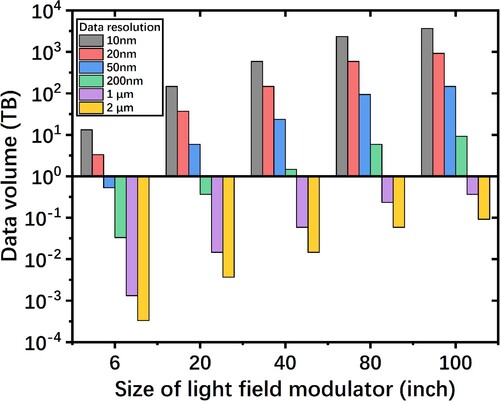
Extensive studies suggest that a breakthrough in the fabrication tool will be detrimental to the advancement of 3D display. However, in spite of the inspirational and rapid-pace developments, micro-/nano-fabrication technology is still in its infancy stage. The manufacture of complex micro- or nano-structures over a large-format remains an extremely difficult science and engineering problem. For example, Figure shows the data volume required for patterning a light field modulator with full coverage of micro-/nano-structures. If the minimum feature size of nanograting is 100 nm, the required data resolution will be 20 nm per pixel or higher. Consequently, the data volume required to produce a 6-inch light field modulator is about 3 TB. At least 3 portable hard disks each with a data volume of 1TB will be needed to store such huge data, not to mention the potential difficulties in data processing and data transmission. In another example, 256-level diffractive optical elements with a minimum feature size of 200 nm correspond to a data volume of 30 TB. In other words, big data is the first nontrivial problem for nanofabrication when the device format goes up to several inches. Efforts are being made in terms of the minimum feature size, patterning precision, fabrication throughput, structural fidelity, and material complexity.
Figure 11. Relationship between the size of light field modulators and the data volume.
Aside from fabrication technologies, 3D display performance is improved from both software and hardware innovations. Light field reconstruction high resolution can be effectively improved by using high refreshable display panel combined with time multiplexing technology or eye tracking methods [Citation65,Citation146]. Spatially variant information density over the observation window improved the resolution at the central region and enlarged the FOV of the system [Citation58]. Deep-learning algorithm were adopted to optimize the display performance by pre-calibration [Citation135,Citation147,Citation148].
Opportunities coexist with challenges. We believe that advances in communication technology, flat panel display screen, and micro-/nano-fabrication technology will lead the innovation and development of light field reconstruction technology for 3D display.
Disclosure statement
No potential conflict of interest was reported by the author(s).
Additional information
Funding
Notes on contributors

Fengbin Zhou
Fengbin Zhou received his B.S. Degree from Nanjing University of Information Science and Technology. He is now a Ph.D candidate in Soochow University. His research focuses on glasses-free 3D display and design of diffractive optical elements.

Wen Qiao
Wen Qiao is a professor and doctoral supervisor from the School of Opto-electronic Science and Engineering, Soochow University. She holds a doctoral degree in entrepreneurship and innovation in Jiangsu Province, a high-level talent in short supply in Suzhou, and one of the first outstanding young scholars of the College of Optics and Electronics. She won the second prize in the Optical Science and Technology Award of the Chinese Optical Society in 2019 and the 22nd China Patent Excellence Award in 2021. In 2013, she graduated from the University of California, San Diego with a Ph.D. degree. In 2014, she joined Soochow University, mainly engaging in research on micro-nano optics, new display, micro-nano manufacturing, and micro-nano sensing technology, among others. As project leader, she undertook more than 10 projects including national projects for the Natural Science Foundation of China and other key national research and development projects. She has published more than 30 papers, including submissions in internationally renowned academic journals such as Advanced Materials, Light Science and Applications, and Nanophotonics.

Linsen Chen
Linsen Chen is a professor and doctoral supervisor at the School of Opto-electronic Science and Engineering, Soochow University. In 2001, he founded SVG Optronics Co., Ltd and served as its chairman. He has been engaged in micro-nano optics and flexible manufacturing research and development, production and sales since then. Related patents provide a framework layout for the core technology methods and functional material design and manufacturing in the field of micro-nano flexible manufacturing, involving the basic methods of micro-nano manufacturing, new micro-nano direct writing lithography device and other fields. He has won numerous recognitions including the China Patent Award, Jiangsu Excellent Patent Gold Award, National Science and Technology Progress Second Prize award, First Prize for Science and Technology of Jiangsu Province, Technological Innovation First Prize award of Enterprises of Jiangsu Province, Technological Invention Second Prize in the Outstanding Scientific and Technological Achievements of the Ministry of Education.
References
- C. Wheatstone, Philos. Trans. R. Soc. London 128, 371–394 (1838). doi:10.1098/rstl.1838.0019.
- F. Zhou, F. Zhou, Y. Chen, J. Hua, W. Qiao, and L. Chen, Optica 9, 288–294 (2022). doi:10.1364/OPTICA.439613.
- F.E.J.J.o.t.F.I. Ives, J. Franklin Inst. 153, 51–52 (1902). doi:10.1016/S0016-0032(02)90195-X.
- S.K. Kim, K.H. Yoon, S.K. Yoon, and H. Ju, Opt. Express 23, 13230–44 (2015). doi:10.1364/OE.23.013230.
- T. Huang, B. Han, X. Zhang, and H. Liao, Opt. Express 27, 20421–20434 (2019). doi:10.1364/OE.27.020421.
- G. Lippmann, La Houille Blanche 7, 204–206 (1908). doi:10.1051/lhb/1908063.
- A. Markman, X. Shen, and B. Javidi, Opt. Lett. 42, 3068–3071 (2017). doi:10.1364/OL.42.003068.
- X. Shen, A. Markman, and B. Javidi, Appl. Opt. 56, D151–D157 (2017). doi:10.1364/AO.56.00D151.
- W. Zhang, X. Sang, X. Gao, X. Yu, C. Gao, B. Yan, and C. Yu, Opt. Express 27, 32810–32822 (2019). doi:10.1364/OE.27.032810.
- Y. Peng, X. Zhou, Y. Zhang, and T. Guo, Appl. Opt. 59, 9104–9107 (2020). doi:10.1364/AO.402704.
- K.C. Kwon, M.U. Erdenebat, A. Khuderchuluun, K.H. Kwon, M.Y. Kim, and N. Kim, Opt. Lett. 46, 5079–5082 (2021). doi:10.1364/OL.436201.
- N.Q. Zhao, J. Liu, and Z.F. Zhao, Opt. Lett. 46, 4240–4243 (2021). doi:10.1364/OL.431415.
- S.-I. Bae, K. Kim, S. Yang, K.-w. Jang, and K.-H. Jeong, Opt. Express 28, 9082–9088 (2020). doi:10.1364/OE.388921.
- W. Wang, S. Li, P. Liu, Y. Zhang, Q. Yan, T. Guo, X. Zhou, and C. Wu, Opt. Laser Technol. 148, 107748 (2022). doi:10.1016/j.optlastec.2021.107748.
- Q. Li, F.-Y. Zhong, H. Deng, and W. He, Liq. Cryst. 1-9 (2022). doi:10.1080/02678292.2022.2032855.
- N.-Q. Zhao, J. Liu, and Z.-F. Zhao, Opt. Letters 46, 4240–4243 (2021). doi:10.1364/OL.431415.
- Z.F. Zhao, J. Liu, Z.Q. Zhang, and L.F. Xu, Opt. Lett 45, 1491–1494 (2020). doi:10.1364/OL.384182.
- X. Sang, X. Gao, X. Yu, S. Xing, Y. Li, and Y. Wu, Opt. Express 26, 8883–8889 (2018). doi:10.1364/OE.26.008883.
- D. Lanman, and D. Luebke, ACM Trans. Graph. 32, 220 (2013). doi:10.1145/2508363.2508366.
- C.-H. Chen, Y.-C. Yeh, and H.-P.D. Shieh, J. Disp. Technol. 4, 92–96 (2008). doi:10.1109/JDT.2007.903145.
- K.-W. Chien, and H.-P.D. Shieh, Appl. Opt. 45, 3106–3110 (2006). doi:10.1364/AO.45.003106.
- N.A. Dodgson, J.R. Moore, S.R. Lang, G. Martin, and P. Canepa, J. Soc. Inf. Disp. 8, 169–176 (2000). doi:10.1889/1.1828713.
- C.-H. Ting, Y.-C. Chang, C.-H. Chen, Y.-P. Huang, and H.-W. Tsai, Appl. Opt. 55, 7922–7928 (2016). doi:10.1364/AO.55.007922.
- Y.S. Hwang, F.K. Bruder, T. Facke, S.C. Kim, G. Walze, R. Hagen, and E.S. Kim, Opt. Express 22, 9820–38 (2014). doi:10.1364/OE.22.009820.
- M. Hirsch, D. Lanman, G. Wetzstein, and R. Raskar, Presented at the ACM SIGGRAPH 2012 Emerging Technologies, Los Angeles, California, 2012.
- D. Lanman, G. Wetzstein, M. Hirsch, W. Heidrich, and R. Raskar, Presented at the Proceedings of the 2011 SIGGRAPH Asia Conference, Hong Kong, China, 2011.
- J. Zhang, Z. Fan, D. Sun, and H. Liao, IEEE Trans. Visualization Comput. Graph. 25, 1603–1614 (2019). doi:10.1109/TVCG.2018.2810279.
- D. Chen, X. Sang, X. Yu, X. Zeng, S. Xie, and N. Guo, Opt. Express 24, 29781–29793 (2016). doi:10.1364/OE.24.029781.
- D. Fattal, Z. Peng, T. Tran, S. Vo, M. Fiorentino, J. Brug, and R.G. Beausoleil, Nature 495, 348–51 (2013). doi:10.1038/nature11972.
- F. Zhou, J. Hua, J. Shi, W. Qiao, and L. Chen, IEEE Photon. Technol. Lett. 32, 283–286 (2020). doi:10.1109/LPT.2020.2971147.
- J. Hua, D. Yi, W. Qiao, and L. Chen, Opt. Commun. 472, 125829 (2020). doi:10.1016/j.optcom.2020.125829.
- J. Shi, J. Hua, F. Zhou, M. Yang, and W. Qiao, Photonics 8 (2021). doi:10.3390/photonics8080337.
- J. Shi, W. Qiao, J. Hua, R. Li, and L. Chen, Nanophotonics 9, 3003–3010 (2020). doi:10.1515/nanoph-2020-0243.
- Z.B. Fan, H.Y. Qiu, H.L. Zhang, X.N. Pang, L.D. Zhou, L. Liu, H. Ren, Q.H. Wang, and J.W. Dong, Light Sci. Appl. 8, 67 (2019). doi:10.1038/s41377-019-0178-2.
- Y. Zhang, D. Yi, W. Qiao, and L. Chen, Opt. Commun. 459, 125034 (2020). doi:10.1016/j.optcom.2019.125034.
- W. Wan, M. Luo, and Y. Su, Opt. Commun. 458, 124857 (2020). doi:10.1016/j.optcom.2019.124857.
- W. Wan, M. Luo, Z. Liu, and Y. Su, Opt. Commun. 459, 124884 (2020). doi:10.1016/j.optcom.2019.124884.
- W. Wan, W. Qiao, D. Pu, and L. Chen, Opt. Lasers Eng. 134, 106258 (2020). doi:10.1016/j.optlaseng.2020.106258.
- W. Wan, L. Lin, M. Luo, Z. Liu, C. Luo, and Y. Su, Opt. Mater. 107, 110011 (2020). doi:10.1016/j.optmat.2020.110011.
- W. Wan, W. Qiao, W. Huang, M. Zhu, Y. Ye, X. Chen, and L. Chen, Opt. express 25, 1114–1122 (2017). doi:10.1364/OE.25.001114.
- W. Wan, W. Qiao, D. Pu, R. Li, C. Wang, Y. Hu, H. Duan, L.J. Guo, and L. Chen, iScience 23, 100773 (2020). doi:10.1016/j.isci.2019.100773.
- S. Yang, X. Sang, X. Yu, X. Gao, L. Liu, B. Liu, and L. Yang, Opt. Express 26, 33013–33021 (2018). doi:10.1364/OE.26.033013.
- W. Wan, W. Qiao, W. Huang, M. Zhu, Y. Ye, X. Chen, and L. Chen, Opt. Express 25, 1114–1122 (2017). doi:10.1364/OE.25.001114.
- X. Zhou, Y. Peng, R. Peng, X. Zeng, Y.-a. Zhang, and T. Guo, ACS Appl. Mater. Interfaces 8, 24248–24255 (2016). doi:10.1021/acsami.6b08278.
- W. Wang, G. Chen, Y. Weng, X. Weng, X. Zhou, C. Wu, T. Guo, Q. Yan, Z. Lin, and Y. Zhang, Sci. Rep. 10, 1–9 (2020). doi:10.1038/s41598-020-68620-z.
- S. Huang, M. Li, L. Shen, J. Qiu, and Y. Zhou, Opt. Laser Technol. 100, 298–303 (2018). doi:10.1016/j.optlastec.2017.10.026.
- H. Xiong, and Z. Wang, J. Micromech. Microeng. 29, 085002 (2019). doi:10.1088/1361-6439/ab1e61.
- H. Yang, C.-K. Chao, M.-K. Wei, and C.-P. Lin, J. Micromech. Microeng. 14, 1197 (2004). doi:10.1088/0960-1317/14/8/012.
- J.-C. Tsai, and Y.-S. Hsu, IEEE Trans. Magn. 47, 598–601 (2011). doi:10.1109/TMAG.2010.2102010.
- E. Roy, B. Voisin, J.F. Gravel, R. Peytavi, D. Boudreau, and T. Veres, Microelectron. Eng. 86, 2255–2261 (2009). doi:10.1016/j.mee.2009.04.001.
- W. Yuan, L.-H. Li, W.-B. Lee, and C.-Y. Chan, Chin. J. Mech. Eng. 31, 1–9 (2018). doi:10.1186/s10033-018-0204-y.
- X. Wang, and H. Hua, Opt. Express 29, 33771–33784 (2021). doi:10.1364/OE.439989.
- G.-J. Lv, J. Wang, W.-X. Zhao, and Q.-H. Wang, Appl. Opt. 52, 6011–6015 (2013). doi:10.1364/AO.52.006011.
- H. Xie, X. Zhao, Y. Yang, J. Bu, Z. Fang, and X. Yuan, Sci. China Technol. Sci. 55, 735–742 (2012). doi:10.1007/s11431-011-4713-5.
- X. Yu, X. Sang, X. Gao, D. Chen, B. Liu, L. Liu, C. Gao, and P. Wang, Opt. Express 27, 16024–16031 (2019). doi:10.1364/OE.27.016024.
- T. Sasagawa, A. Yuuki, S. Tahata, O. Murakami, and K. Oda, SID Symp. Dig. Tech. Pap. 34, 399–401 (2003). doi:10.1889/1.1832296.
- X.T. Zhou, Y.L. Weng, Y.Y. Peng, G.X. Chen, J.P. Lin, Q. Yan, Y.A. Zhang, and T.L. Guo, Optik 157, 532–539 (2018). doi:10.1016/j.ijleo.2017.11.117.
- J. Hua, E. Hua, F. Zhou, J. Shi, C. Wang, H. Duan, Y. Hu, W. Qiao, and L. Chen, Light Sci. Appl. 10, 213 (2021). doi:10.1038/s41377-021-00651-1.
- A.Y. Yi, and L. Li, Opt. Lett. 30, 1707–1709 (2005). doi:10.1364/ol.30.001707.
- J. Yan, Z. Zhang, T. Kuriyagawa, and H. Gonda, Int. J. Adv. Manuf. Technol. 51, 957–964 (2010). doi:10.1007/s00170-010-2695-2.
- G.S. Hong, and Y. San Wong, Int. J. Mach. Tools Manuf. 52, 13–23 (2012). doi:10.1016/j.ijmachtools.2011.08.010.
- X. Zhang, F. Fang, L. Yu, L. Jiang, and Y. Guo, Opt. Eng. 52, 023401 (2013). doi:10.1117/1.OE.52.2.023401.
- Y.B. Kim, J. Park, W.S. Lee, and J.K. Lee, Mater. Manuf. Processes 36, 1171–1177 (2021). doi:10.1080/10426914.2021.1885714.
- P. Wang, X. Sang, X. Yu, X. Gao, B. Yan, B. Liu, L. Liu, C. Gao, Y. Le, Y. Li, and J. Du, Opt. Express 27, 34442–34453 (2019). doi:10.1364/OE.27.034442.
- B. Liu, X. Sang, X. Yu, X. Gao, L. Liu, C. Gao, P. Wang, Y. Le, and J. Du, Opt. Express 27, 35728–35739 (2019). doi:10.1364/OE.27.035728.
- L. Yang, X. Sang, X. Yu, B. Liu, B. Yan, K. Wang, and C. Yu, Opt. Express 26, 34412–34427 (2018). doi:10.1364/OE.26.034412.
- H.M. Leung, G. Zhou, H. Yu, F.S. Chau, and A.S. Kumar, J. Micromech. Microeng. 20, 025021 (2010). doi:10.1088/0960-1317/20/2/025021.
- C. Chan, L. Li, W. Lee, W. Yuan, and Y. Liu, J. Mech. Eng. 52, 50–57 (2016). doi:10.3901/JME.2016.17.050.
- Z. Zhu, S. To, and S. Zhang, Opt.Express 23, 20593–20604 (2015). doi:10.1364/OE.23.020593.
- S. Scheiding, A.Y. Yi, A. Gebhardt, L. Li, S. Risse, R. Eberhardt, and A. Tünnermann, Opt. Express 19, 23938–23951 (2011). doi:10.1364/OE.19.023938.
- Z. Zhu, S. To, W.-L. Zhu, and P. Huang, Int. J. Mach. Tools Manuf. 122, 98–105 (2017). doi:10.1016/j.ijmachtools.2017.06.004.
- L. Yang, X. Sang, X. Yu, B. Yan, K. Wang, and C. Yu, Opt. Express 27, 15679–15692 (2019). doi:10.1364/OE.27.015679.
- S. To, Z. Zhu, and H. Wang, CIRP Ann. 65, 475–478 (2016). doi:10.1016/j.cirp.2016.04.047.
- J. Alamán, R. Alicante, J.I. Peña, and C. Sánchez-Somolinos, Materials 9, 910 (2016). doi:10.3390/ma9110910.
- X. Zhu, Q. Xu, Y. Hu, H. Li, F. Wang, Z. Peng, and H. Lan, Opt. Laser Technol. 115, 118–124 (2019). doi:10.1016/j.optlastec.2019.02.014.
- V. Vespini, S. Coppola, M. Todino, M. Paturzo, V. Bianco, S. Grilli, and P. Ferraro, Lab Chip 16, 326–333 (2016). doi:10.1039/C5LC01386K.
- C.-H. Tien, C.-H. Hung, and T.-H. Yu, J. Disp. Technol. 5, 147–151 (2009). doi:10.1109/JDT.2009.2013874.
- D.L. MacFarlane, V. Narayan, J.A. Tatum, W.R. Cox, T. Chen, and D.J. Hayes, IEEE Photon. Technol. Lett. 6, 1112–1114 (1994). doi:10.1109/68.324684.
- J.Y. Kim, N.B. Brauer, V. Fakhfouri, D.L. Boiko, E. Charbon, G. Grutzner, and J. Brugger, Opt. Mater. Express 1, 259–269 (2011). doi:10.1364/OME.1.000259.
- Y. Peng, R. Peng, Z. Chu, X. Zhou, Y. Zhang, and T. Guo, J. Disp. Technol. 12, 822–827 (2016). doi:10.1109/JDT.2016.2542880.
- W. Wang, G. Chen, Y. Weng, X. Weng, X. Zhou, C. Wu, T. Guo, Q. Yan, Z. Lin, and Y. Zhang, Sci. Rep. 10, 11741 (2020). doi:10.1038/s41598-020-68620-z.
- Z.D. Popovic, R.A. Sprague, and G.A. Neville Connell, Appl. Opt. 27, 1281–1284 (1988). doi:10.1364/AO.27.001281.
- J. Zhu, M. Li, J. Qiu, and H. Ye, Microsyst. Technol. 25, 1235–1241 (2019). doi:10.1007/s00542-018-4226-2.
- R. Kirchner, and H. Schift, Mater. Sci. Semicond. Process. 92, 58–72 (2019). doi:10.1016/j.mssp.2018.07.032.
- J. Qiu, M. Li, H. Ye, C. Yang, and C. Shi, Appl. Opt. 57, 7296–7302 (2018). doi:10.1364/AO.57.007296.
- M. Wang, W. Yu, T. Wang, X. Han, E. Gu, and X. Li, RSC Adv. 5, 35311–35316 (2015). doi:10.1039/C5RA00957J.
- H. Oh, G. Kim, H. Seo, Y. Song, K. Lee, and S.S. Yang, Sens. Actuators A: Phys. 164, 161–167 (2010). doi:10.1016/j.sna.2010.10.003.
- D. Jucius, V. Grigaliūnas, A. Lazauskas, E. Sapeliauskas, B. Abakevičienė, S. Smetona, and S. Tamulevičius, Microsyst. Technol. 23, 2193–2206 (2017). doi:10.1007/s00542-016-2975-3.
- C.-P. Lin, H. Yang, and C.-K. Chao, J. Micromech. Microeng. 13, 775 (2003). doi:10.1088/0960-1317/13/5/333.
- K. Kim, K.W. Jang, J.K. Ryu, and K.H. Jeong, Light Sci. Appl. 9, 28 (2020). doi:10.1038/s41377-020-0261-8.
- S.I. Bae, K. Kim, K.W. Jang, H.K. Kim, and K.H. Jeong, Adv. Opt. Mate. 9, 2001657 (2021). doi:10.1002/adom.202001657.
- M.N. Hasan, M.-U. Haque, J. Trisno, and Y.-C. Lee, J. Micro/Nanolithogr. MEMS MOEMS 14, 043505 (2015). doi:10.1117/1.JMM.14.4.043505.
- K. Zhong, H. Zhang, and Y. Gao, Optik 142, 243–248 (2017). doi:10.1016/j.ijleo.2017.05.069.
- C. Hong, and X. Zhang, Nanophotonics 7, 1819–1825 (2018). doi:10.1515/nanoph-2018-0091.
- Z. Zhang, Y. Gao, N. Luo, and K. Zhong, AIP Adv. 6, 015319 (2016). doi:10.1063/1.4941356.
- N. Luo, and Z. Zhang, J. Micromech. Microeng. 27, 035015 (2017). doi:10.1088/1361-6439/aa596a.
- A. Hohnholz, K. Obata, Y. Nakajima, J. Koch, M. Terakawa, O. Suttmann, and L. Overmeyer, Appl. Phys. A 125, 120 (2019). doi:10.1007/s00339-018-1902-0.
- D. Wu, J.-N. Wang, L.-G. Niu, X.L. Zhang, S.Z. Wu, Q.-D. Chen, L.P. Lee, and H.B. Sun, Adv. Opt. Mater. 2, 751–758 (2014). doi:10.1002/adom.201400175.
- K. Totsu, K. Fujishiro, S. Tanaka, and M. Esashi, Sens. Actuators A: Phys. 130-131, 387–392 (2006). doi:10.1016/j.sna.2005.12.008.
- Q. Deng, Y. Yang, H. Gao, Y. Zhou, Y. He, and S. Hu, Micromachines 8 (2017). doi:10.3390/mi8100314.
- D.-H. Dinh, H.-L. Chien, and Y.-C. Lee, Opt. Laser Technol. 113, 407–415 (2019). doi:10.1016/j.optlastec.2019.01.001.
- J.-B. Kim, and K.-H. Jeong,, Opt. Express 25, 16854–16859 (2017). doi:10.1364/OE.25.016854.
- T. Yang, Y.H. Liu, Q. Mu, M. Zhu, D. Pu, L. Chen, and W. Huang, Opt. Express 27, 7513–7522 (2019). doi:10.1364/OE.27.007513.
- R.J. Lin, V.C. Su, S. Wang, M.K. Chen, T.L. Chung, Y.H. Chen, H.Y. Kuo, J.W. Chen, J. Chen, Y.T. Huang, J.H. Wang, C.H. Chu, P.C. Wu, T. Li, Z. Wang, S. Zhu, and D.P. Tsai, Nat. Nanotechnol. 14, 227–231 (2019). doi:10.1038/s41565-018-0347-0.
- V.R. Manfrinato, L. Zhang, D. Su, H. Duan, R.G. Hobbs, E.A. Stach, and K.K. Berggren, Nano Lett. 13, 1555–1558 (2013). doi:10.1021/nl304715p.
- M.J. Burek, and J.R. Greer, Nano Lett. 10, 69–76 (2010). doi:10.1021/nl902872w.
- J. Yang, B. Cord, H. Duan, K.K. Berggren, J. Klingfus, S.W. Nam, K.B. Kim, and M.J.J.J.o.v.s. Rooks, J. Vac. Sci. Technol. B 27, 2622–2627 (2009). doi:10.1116/1.3253652.
- J. Joo, B.Y. Chow, and J.M. Jacobson, Nano Lett. 6, 2021–5 (2006). doi:10.1021/nl061211q.
- H. Namatsu, K. Yamazaki, and K.J.J.v.s.t.b. Kurihara, J. Vac. Sci. Technol. B 18, 780–784 (2000). doi:10.1116/1.591276.
- H. Deng, C. Chen, M.-Y. He, J.-J. Li, H.-L. Zhang, and Q.-H. Wang, J. Opt. Soc. Am. A 36, 588–593 (2019). doi:10.1364/JOSAA.36.000588.
- S. Lee, C. Jang, J. Cho, J. Yeom, J. Jeong, and B. Lee, Appl. Opt. 55, A95–A103 (2016). doi:10.1364/AO.55.000A95.
- B.J. Jackin, L. Jorissen, R. Oi, J.Y. Wu, K. Wakunami, M. Okui, Y. Ichihashi, P. Bekaert, Y.P. Huang, and K. Yamamoto, Opt. Lett. 43, 3738–3741 (2018). doi:10.1364/OL.43.003738.
- S. Lee, C. Jang, S. Moon, J. Cho, and B. Lee, ACM Trans. Graph. 35, 60 (2016). doi:10.1145/2897824.2925971.
- F. Lu, J. Hua, F. Zhou, Z. Xia, R. Li, L. Chen, and W. Qiao, Opt. Express 30, 15929–15938 (2022). doi:10.1364/OE.456824.
- C. Jang, C.-K. Lee, J. Jeong, G. Li, S. Lee, J. Yeom, K. Hong, and B. Lee, Appl. Opt. 55, A71–A85 (2016). doi:10.1364/AO.55.000A71.
- W. Wan, W. Qiao, W. Huang, M. Zhu, Z. Fang, D. Pu, Y. Ye, Y. Liu, and L. Chen, Opt. Express 24, 6203–12 (2016). doi:10.1364/OE.24.006203.
- Z. He, G. Tan, D. Chanda, and S.-T. Wu, Opt. Express 27, 11472–11491 (2019). doi:10.1364/OE.27.011472.
- S. Maruo, O. Nakamura, and S. Kawata, Opt. Lett. 22, 132–134 (1997). doi:10.1364/OL.22.000132.
- F. Claeyssens, E.A. Hasan, A. Gaidukeviciute, D.S. Achilleos, A. Ranella, C. Reinhardt, A. Ovsianikov, X. Shizhou, C. Fotakis, M. Vamvakaki, B.N. Chichkov, and M. Farsari, Langmuir 25, 3219–3223 (2009). doi:10.1021/la803803m.
- G. Kumi, C.O. Yanez, K.D. Belfield, and J.T. Fourkas, Lab Chip 10, 1057–1060 (2010). doi:10.1039/B923377F.
- S. Rekštytė, T. Jonavičius, D. Gailevičius, M. Malinauskas, V. Mizeikis, E.G. Gamaly, and S. Juodkazis, Adv. Opt. Mater. 4, 1209–1214 (2016). doi:10.1002/adom.201600155.
- Z. Faraji Rad, P.D. Prewett, and G.J. Davies, Microsyst. Nanoeng. 7, 71 (2021). doi:10.1038/s41378-021-00298-3.
- A.S. Cordeiro, I.A. Tekko, M.H. Jomaa, L. Vora, E. McAlister, F. Volpe-Zanutto, M. Nethery, P.T. Baine, N. Mitchell, D.W. McNeill, and R.F. Donnelly, Pharm. Res 37, 174 (2020). doi:10.1007/s11095-020-02887-9.
- J. Li, P. Fejes, D. Lorenser, B.C. Quirk, P.B. Noble, R.W. Kirk, A. Orth, F.M. Wood, B.C. Gibson, D.D. Sampson, and R.A. McLaughlin, Sci. Rep. 8, 14789 (2018). doi:10.1038/s41598-018-32407-0.
- J.Y.E. Chan, Q. Ruan, M. Jiang, H. Wang, H. Wang, W. Zhang, C.-W. Qiu, and J.K.W. Yang, Nat. Commun. 12, 1–9 (2021). doi:10.1038/s41467-021-23964-6.
- K. Obata, J. Koch, U. Hinze, and B.N. Chichkov, Opt. Express 18, 17193–17200 (2010). doi:10.1364/OE.18.017193.
- W. Xiong, Y.S. Zhou, X.N. He, Y. Gao, M. Mahjouri-Samani, L. Jiang, T. Baldacchini, and Y.F. Lu, Light: Sci. Appl. 1, e6–e6 (2012). doi:10.1038/lsa.2012.6.
- W. Zhang, G. Zhu, X. Zhu, and C. Du, Front. Phys. 8 (2020). doi:10.3389/fphy.2020.00267.
- L. Zhang, N.J. Naples, W. Zhou, and A.Y. Yi, J. Micromech. Microeng. 29, 065004 (2019). doi:10.1088/1361-6439/ab10ff.
- E.A. Sanchez, M. Waldmann, and C.B. Arnold, Appl. Opt. 50, 1974–1978 (2011). doi:10.1364/AO.50.001974.
- C. Tien, C. Hung, and T. Yu, J. Disp. Technol. 5, 147–151 (2009). doi:10.1109/JDT.2009.2013874.
- S.G. Heo, D. Jang, H.J. Koo, and H. Yoon, Opt. Express 27, 3439–3447 (2019). doi:10.1364/OE.27.003439.
- H.-D. Kim, G.-W. Yoon, J. Yeon, J.-H. Lee, and J.-B. Yoon, J. Micromech. Microeng. 22, 045002 (2012). doi:10.1088/0960-1317/22/4/045002.
- C.-P. Lin, H. Yang, and C.-K. Chao, J. Micromech. Microeng. 13, 775–781 (2003). doi:10.1088/0960-1317/13/5/333.
- E. Tseng, S. Colburn, J. Whitehead, L. Huang, S.-H. Baek, A. Majumdar, and F. Heide, Nat. Commun. 12, 6493 (2021). doi:10.1038/s41467-021-26443-0.
- E. Højlund-Nielsen, T. Greibe, N.A. Mortensen, and A. Kristensen, Microelectron. Eng. 121, 104–107 (2014). doi:10.1016/j.mee.2014.03.025.
- C. Maibohm, O.F. Silvestre, J. Borme, M. Sinou, K. Heggarty, and J.B. Nieder, Sci. Rep. 10, 8740 (2020). doi:10.1038/s41598-020-64955-9.
- V.F. Paz, M. Emons, K. Obata, A. Ovsianikov, S. Peterhänsel, K. Frenner, C. Reinhardt, B. Chichkov, U. Morgner, and W. Osten, J. Laser Appl. 24, 042004 (2012). doi:10.2351/1.4712151.
- C.N. LaFratta, and T. Baldacchini, Micromachines 8 (2017). doi:10.3390/mi8040101.
- A. Maimone, and J. Wang, ACM Trans. Graph. 39, 67 (2020). doi:10.1145/3386569.3392416.
- B. Tibor, Presented at the Electronic Imaging 2006, Proc.SPIE, California, United States, 2006.
- https://holografika.com/722rc/
- https://lookingglassfactory.com/portrait
- https://www.continental.com/en-us/press/press-releases/continental-leia-3d-lightfield-display/
- https://www.leiainc.com/#Product
- K.H. Yoon, M.K. Kang, H. Lee, and S.K. Kim, Appl. Opt. 57, A101–A117 (2018). doi:10.1364/AO.57.00A101.
- X. Dun, H. Ikoma, G. Wetzstein, Z. Wang, X. Cheng, and Y. Peng, Optica 7, 913–922 (2020). doi:10.1364/OPTICA.394413.
- Q. Sun, C. Wang, Q. Fu, X. Dun, and W. Heidrich, ACM Trans. Graph. 40, 1–13 (2021). doi:10.1145/3450626.3459674.