
 ?Mathematical formulae have been encoded as MathML and are displayed in this HTML version using MathJax in order to improve their display. Uncheck the box to turn MathJax off. This feature requires Javascript. Click on a formula to zoom.
ABSTRACT
High-performance electrochromic devices (ECDs) were fabricated by introducing indium tin oxide/silver/indium tin oxide (IAI) multilayers as a transparent conducting oxide (TCO) electrode in conjunction with microstructural tailoring of tungsten trioxide (WO3) as an electrochromic (EC) layer. A 15-nm-thick Ag film with a preferential orientation of (111) and smooth morphology resulted in a high optical transmittance of 90.9% and sheet resistance 16.7 Ω/sq, making it a suitable TCO. In addition, the open network WO3 film used as an EC layer was deposited by carefully controlling the chamber pressure during the sputtering process. A high chamber pressure (2.0 Pa) resulted in a WO3 film with the lowest mass density (5.72 g/cm3) and a rough morphology. Half-cell ECDs consisting of a TCO bottom electrode (BE)/WO3 stack immersed in LiClO4 electrolyte were fabricated to verify the impact of using the IAI multi-layer stack and tailored WO3 film as a TCO and EC layer, respectively. Significant enhancement in terms of coloration efficiency was achieved for the ECDs by adopting the IAI TCO and open network WO3 EC layer compared to counterpart devices with an ITO TCO or dense WO3 EC film. This can be explained by the facile carrier extraction (injection) and transport of Li ions.
1. Introduction
Electrochromic devices (ECDs) are key technologies for energy-saving smart windows, next-generation information displays, switchable mirrors, and wearable electronics because they efficiently change their optical properties including transmittance, reflectance, and color under a low driving voltage range [Citation1,Citation2]. A typical ECD consists of an electrochromic (EC) layer, an electrolyte layer, and an ion storage (IS) layer sandwiched between two transparent conducting electrodes (TCOs) [Citation3]. The injection/extraction of charge into an electrochromic layer under an applied electric field between the anode and cathode modulates its band gap, which changes the optical colligative properties. The performance of the ECD is strongly dependent on the structural and electrical properties of the transparent electrode and EC layer itself. First, the TCO film significantly affects the transmittance of the entire ECD, which provided a charge carrier to the electrochromic layer from an external circuit. Indium-tin oxide (ITO) is a representative TCO material used for commercial optoelectronic devices. It has a relatively low resistance (<10−3 Ωcm) and high transmittance to visible light (>80%) due to its wide bandgap (∼4.8 eV) [Citation4]. However, a rather thick ITO is required to realize an acceptable low sheet resistance due to its larger electrical resistivity (by approximately two orders of magnitudes) compared to metals (2.5 × 10⁻⁶ Ωcm) such as Al and Cu. This increases the material cost and reduces the transmittance of visible light due to the interference effect [Citation5,Citation6]. This trade off problem between the electrical conductivity and optical transmittance of the ITO film can be mitigated using a multi-layer electrode scheme where a thin metal layer is inserted in the ITO electrode stacks [Citation7–9]. The ITO/metal/ITO stack has a higher electrical conductivity compared to that of the single ITO film under an identical optical transmittance condition where the reflection from the metal layer in the visible range can be effectively suppressed for the ITO/metal/ITO stack. For this reason, various TCO/metal/TCO multi-layer structures have been investigated including ITO/metal (Au, Ag, Cu or Mo)/ITO [Citation10,Citation11], ZnO/Cu/ZnO [Citation12], IZO/Au/IZO [Citation13], ZnO/Ag/ZnO [Citation14], AZO/Ag/AZO [Citation15] and ZTO/Ag /ZTO [Citation16]. An ITO/metal/ITO stack has been extensively examined in organic light emitting diodes [Citation7,Citation17,Citation18] and solar cells [Citation19–22]. However, case studies of ITO/metal/ITO stacks in ECD as a transparent conducting oxide (TCO) electrode are surprisingly limited. Second, the EC is a critical component governing the ECD performance through reversible insertion (or extraction) of external protons or ions into (or from) the host lattice. Among various EC materials, tungsten trioxide (WO3) has attracted much attention due to its reversible color conversion capability from optical transparency to a deep blue color as well as its superior electrochemical stability compared to the counterparts of organic EC materials [Citation23,Citation24]. However, the low coloration efficiency (CE) (<30.0 cm2C−1) and slow switching speed (>10.0 s) of WO3 films remain major obstacles their use as an EC layer in practical applications [Citation25,Citation26]. Thus, various approaches to enhance the EC performance have been proposed including tailoring the film structure, electronic structure, and crystalline structure [Citation27–29]. In particular, the rather porous nano/microstructure of WO3 films with a high specific surface area improved the modulation efficiencies of transmittance and CE values by increasing electrostatic contact with the electrolyte compared to dense WO3 films [Citation27,Citation28]. For example, Yang et al. re-ported that a porous WO3 film prepared by a template-assisted sol–gel method exhibited a high CE (50.1 cm2C−1) and fast switching speed (5.1 s for coloration rate and 8.7 s for bleaching rate) [Citation30]. In contrast, a magnetron sputtering method is known to easily produce the amorphous WO3 film with few defects and high coloration efficiency. Although many EC studies have been reported, research on how the ITO/Ag/ITO multi-layer structure impacts electrochromic performance with the porous WO3 film as an EC layer remains lacking.
In this study, Ag thickness-dependent structural, electrical, and optical properties of the ITO/Ag/ITO (IAI) multi-layer structures were examined. The effect of the WO3 film’s microstructure on the electrical and optical properties of the EC devices with the optimized IAI multi-layer structure was also investigated, for which the porous structure of WO3 film was tailored by modifying the chamber pressure during sputtering. The electrochemical and optical properties were characterized by cyclic voltammetry, chronoamperometry and spectroscopic measurements. The light modulation of the WO3 electrochromic layer was improved substantially by using the IAI multi-layer electrode and porous structure of WO3 EC simultaneously.
2. Experimental section
2.1. Fabrication of ITO/Ag/ITO electrode stack
Transparent conductive IAI electrodes with varying Ag thickness were prepared on glass substrates by DC magnetron sputtering at room temperature in a pure argon (Ar, 99.999%) atmosphere. The ITO target (90 wt.% In) with the 3-inch diameter and purity of 99.99% (4N) was used to deposit the ITO film. The IAI stack was sequentially deposited in one chamber without breaking the vacuum. The target powers of the ITO and Ag were 100 and 105 W during film preparation, respectively. The chamber base and working pressure were 4 × 10⁻⁴ and 0.43 Pa, respectively. The thickness of the bottom and top ITO layers was fixed to 40 nm, where the thickness of the inserted Ag film was 0, 13, 15, 17 or 19 nm. The substrate was rotated during film deposition to ensure good thickness uniformity.
2.2. Preparation of inorganic nano-porous tungsten oxide electrochromic layer
WO3 thin films were deposited on IAI multilayers by reactive DC magnetron sputtering using a W metal target (99.99%) and oxygen plasma under an Ar atmosphere at room temperature. The base pressure of the sputtering chamber was ∼ 4 × 10⁻⁴ Pa. The W target was pre-sputtered for 10 min prior to WO3 deposition to eliminate surface contamination such as WOx. The input gas mixture of Ar and O2 with a 9:1 ratio was provided in the sputtering chamber where the chamber pressure varied from 1.0 to 2.0 Pa to control the WO3 film’s microstructure. The DC power of the W target was fixed to 80 W, and the sample stage was continuously rotated to ensure film uniformity during reactive sputtering. More detailed deposition parameters for each layer of ECD are listed in Table .
Table 1. Detailed deposition parameters for each layer of ECD.
2.3. Characterization and analysis methods
Spectroscopic ellipsometry (SE, Elli-SE, Ellipso Technology, South Korea) was used to measure the film thickness. The structural properties of different films were characterized by X-ray diffraction (GIXRD, SmartLab, Rigaku, Japan) equipped with a Cu Kα source (40 KV, 30 mA). The morphological properties of various thin films were characterized by atomic force microscopy (AFM, Multimode 8, Brucker). The cross-sectional images of the ECD cell were obtained by field-emission scanning electron microscopy (FE-SEM, Verios G4 UC, FEI Co.). The densities of the films were analyzed by high-resolution X-ray reflectivity (XRR, SmartLab, Rigaku), where the XRR raw data were fitted using GlobalFit analysis software. Resistivity and carrier concentration of the transparent ITO and ITO/Ag/ITO films were characterized by measuring Hall effect using the van der Pauw technique (HL5500, BioRad). Optical transmission spectra were acquired with a UV/visible spectrometer (Thermo scientific, Evolution 220) in the wavelength range of 300–800 nm at room temperature.
The schematic of the fabricated ECD system is shown in Figure S1 in Supporting Information (SI). The electrochemical properties of ECDs were investigated by cyclic voltammetry (CV) and chronoamperometry (CA) techniques using an electrochemical workstation (BioLogic, SP-50). The cell size of the ECD was 2 cm × 4 cm. The schematic of the three-electrode system used for the CV and CA measurements is presented in Figure S2 (SI), and the system was connected to a potentiostat and a computer. The EC testing of LixWO3(WO3:Li) samples in 1.0 M liquid-electrolyte of LiClO4/PC solution was performed using a three-electrode cell, comprising a working electrode (WO3 electrode film on ITO/glass), a counter-electrode (Pt wire) and a reference electrode (Ag/AgCl). The potential voltage windows for CV and CA measurements were −1.0 V (tinted) and +1.0 V (bleached). In CA cycling measurements, the duration was 30 s for both the staining and bleaching phases. The scan rate for CV measurements was 50 mV/s. Light transmission spectra (300 nm–900 nm) of the ECDs in the bleached and pigmented states were acquired using a UV–Vis spectrophotometer. To ensure that the ECDs were sufficiently stained and bleached, the transmittance spectra were measured after applying a voltage of ±1.0 V to the ECDs for 30 s each for staining and bleaching.
3. Results and discussion
3.1. Effect of ITO/Ag/ITO electrode stack on the performance of ECDs
Figure (a–d) depicts the evolution of SEM surface morphologies of Ag films on the ITO/Si substrate as a function of Ag deposition time. When the Ag deposition time (tdep) is short (∼13 s), the deposited film had discontinuous, isolated island morphologies (Figure (a)). This suggests poor wetting between metallic Ag and ITO substances [Citation31]. The Ag film becomes continuous and completely covers the underlying ITO film with increasing tdep (≥15 s). Thus, the smooth morphologies of the Ag films with thicknesses of 15 and 17 nm were obtained, corresponding to tdep of 15 and 17 s, respectively. However, the prolonged Ag deposition of 19 s caused surface roughening in the resulting 19 nm-thick Ag film as shown in Figure (d). This thickness-induced morphology roughening phenomena can be attributed to the buildup and release of residual internal stress involving the formation of protrusion [Citation32]. These features were reflected in the roughness variations of deposited Ag films with different thicknesses as shown in Figure (e–h). The Ag film at tdep = 13 s suffered from huge root-means-square (RMS) values of 3.7 nm due to the island-like discontinuous morphologies. Smaller RMS values of 0.47 and 0.48 nm were obtained for the Ag films at tdep = 15 and 17 s by virtue of the formation of a continuous smooth film. Conversely, the Ag film at the tdep = 19 s had an increased RMS value of 0.76 nm because of the roughening morphology (Figure (h)).
Figure 1. Evolution in the SEM and AFM surface morphologies of the Ag film deposited on the ITO/Si substrate as a function of Ag deposition time (tdep): tdep = (a)–(e) 13 s, (b)–(f) 15 s, (c)–(g) 17 s and (d)–(h) 19 s.
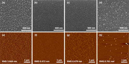
Figure shows the GI-XRD patterns of the control ITO and IAI multi-layer films with Ag films with varying thickness. The control ITO film had discernible diffraction peaks at 30.5° and 51°, which were assignable to bixbyite (222) and (400) reflections. In contrast, the IAI multi-layer films had additional diffraction peaks at 38.1°, which correspond to (111) of the face-centered-cubic Ag phase. It is noted that the (111) reflection of Ag phase in IAI multi-layer samples gradually increased with increasing Ag thickness, whereas the other diffraction peaks had rather thickness-independent intensities. The development of (111) preferential orientation can be explained by the following thermodynamic reasoning. The (111) face has the smallest interface energy in the face-centered-cubic Ag crystal, which means that (111) faces are dominant with increasing tdep to minimize the total Gibbs free energy of the Ag film.
Figure 2. Variations in XRD patterns of IAI films inserted with Ag films of varying thickness.
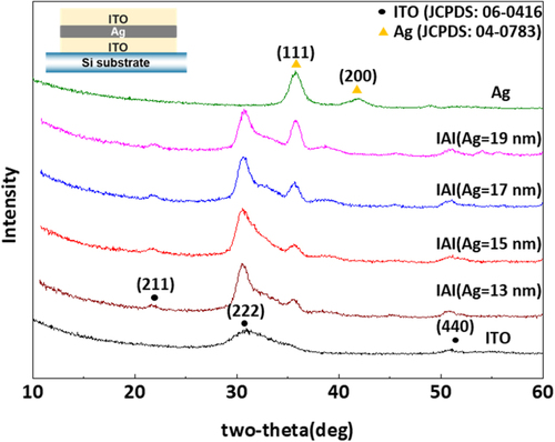
Figure (a) shows the variations in resistivity (ρ) and carrier concentration (ne) of the IAI multi-layer structure as a function of tdep. The control ITO film (80 nm) had the largest ρ value of 1.76 × 10⁻³ Ωcm. The IAI sample with an Ag interlayer at tdep = 13 s exhibited a slightly reduced ρ value of 1.58 × 10⁻³ Ωcm. The modest improvement should be attributed to the discontinuous, island microstructure of the Ag layer. Significant improvement (1.43–1.58 × 10⁻⁴ Ωcm) in terms of ρ value was observed for the IAI samples with Ag films at tdep = 15 and 17 s. This was attributed to a change from the discontinuous island-like structure to the continuous formation of Ag film [Citation33]. The dynamic change in ρ value of IAI multi-layer films comes from the ne variation. It increased from 1.1 × 1020 cm−3 (control ITO sample) to 5.2 × 1021 cm−3 for the IAI sample with ITO film at tdep = 19 s. The optimal transmittance of the IAI multilayers depending on the tdep was examined as shown in Figure (b). The control ITO sample had an average transmittance near 90% for the wavelength range from 300 to 800 nm. A reduced transmittance of 64% was obtained for the IAI sample with an Ag interlayer at tdep = 13 s due to the light scattering by the isolated island-shaped Ag interlayer. In contrast, the IAI sample with an Ag interlayer at tdep = 15 s exhibited a higher transmittance (∼91%) for visible light, which is consistent with its structural properties as mentioned earlier. This high transmittance suggests that the Ag interlayer at tdep = 15 s intercalated between two ITO layers has an anti-reflection effect with the upper and lower ITO layers at the given specific thickness [Citation34]. The IAI sample with the thickest Ag film at tdep = 19 s, however, showed a drop in the transmittance (∼67%) due to its strong absorption of visible light. The figure of merit (FOM) of the IAI multi-layer structures, which can be a good indicator of the optimal capability of high transmittance and low resistivity, was calculated using the Haacke equation [Citation35] as follows:
(1)
(1) Here, ΦTC is the FOM, T is the optical transmittance of the IAI multi-layer structure at a wavelength of 550 nm, and Rs is the sheet resistance. The maximum value of ΦTC was 23.1 × 10⁻³ Ω−1 for the IAI multi-layer with an Ag film at tdep = 15 s with an optical transmittance of 90.9% and sheet resistance of 16.7 Ω/cm2 as shown in Figure (c) and Table . We anticipated that the IAI multiplayer with an Ag film at the tdep = 15 s (hereafter referred to as IAI-15s) would exhibit the best performance for ECD applications, which is why we chose the IAI-15 stack as a benchmarking electrode to compare with the control ITO electrode.
Figure 3. (a) Resistivity, carrier concentration of the IAI multilayers as a function of Ag thickness. (b) Optical transmittance spectra of the IAI multilayers as a function of Ag thickness. (c) Figure of merit and sheet resistance of the IAI multi-layer structures as a function of Ag thickness.
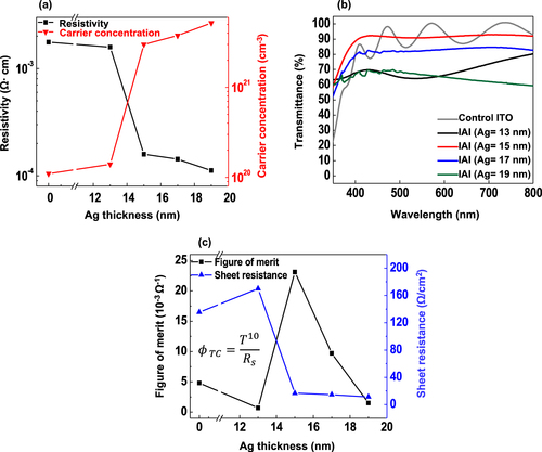
Table 2. The sheet resistance, optical transmittance, and the figure of merit of the IAI multilayers with Ag deposition time varying from 0 s to 19 s.
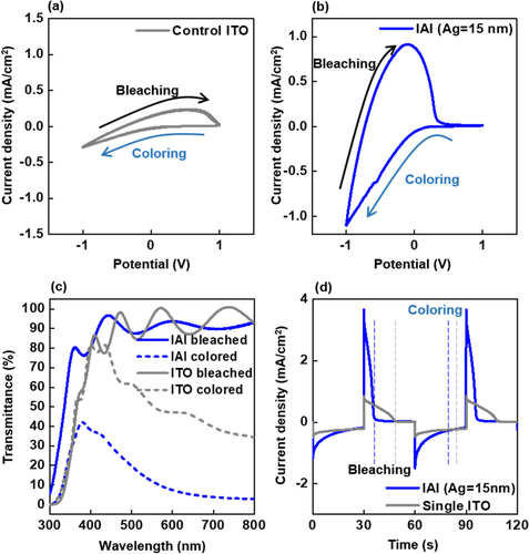
The feasibility of using IAI multi-layer stack as a transparent conductive electrode was tested by fabricating an ECD cell with the WO3 layer as an EC layer. Figure (a) and (b) show the CV characteristics of the ECDs with the control ITO and IAI-15s bottom electrode (BE), respectively. When the BE voltage incrementally changed from 0 V to −1 V, the current density (J) for the given half-cell increases negatively as shown in Figure (a) and (b). This is referred to as a coloring process [see the details related to the experimental setup (Figure S2) in SI]. The slope between J and V during the coloring process significantly increased for the ECD with the IAI-15 BE compared to that for the device with the ITO BE, which can be explained by the ∼9-fold smaller resistance of the IAI-15 electrode (∼16 Ω/sq). When the BE voltage increased from −1 V to 1 V as a function of time, the reversal flow of Li ion occurs through the given cell, leading to a positive incremental change in J with respect to the applied V (ΔJ/ΔV). This de-intercalation corresponds to the bleaching process, which is indicated in Figure (a) and (b). The rapid slope (ΔJ/ΔV = ∼1.98 mA/cm2 V) for the device with IAI-15 BE compared to that (ΔJ/ΔV = ∼0.42 mA/cm2V) of the ITO control device indicates the efficient bleaching capability for the same reasons. The detailed electro-chemical model responsible for the coloring and bleaching process will be addressed later. The dolphin-shaped area, which is the path of the coloring and bleaching process, is known to be a good indicator of the EC performance. Obviously, the dolphin-shaped area was greatly enhanced for the ECD with the IAI-15 BE (Figure (a) and (b)). Figure (c) shows the variation in the transmittance (T) spectra of ECDs with control ITO and IAI BE in the colored and bleached states. Both cells had comparable transmittance values under the bleached state for visible light. Conversely, the transmittance near 550 nm for the ECD with the IAI BE in the coloring state dropped to ∼10%, whereas the ECD with control ITO BE had a transmittance of ∼50%. Thus, the larger optical modulation range (86.2%) of ECD with the IAI BE electrode compared to that for the control ITO cell should be attributed to the efficient coloring capability. Figure (d) showed the kinetic behavior for both ECDs during the bleaching and coloring states by providing a time-dependent rectangular voltage pulse (amplitude ± 1 V, 1 cycle duration = 60 s, also see Figure S3, SI). Response time is defined as the time needed to reach 90% of the transmittance modulation ΔT of the given ECD at a fixed wavelength of 550 nm. The coloration response times for the ECDs with the control ITO and IAI BE were 20 and 16 s, respectively (Figure (d)). The falling time values of J with increasing time for the ECDs with control ITO and IAI BE during the bleaching process were approximately 20 and 7 s, respectively. The rapid bleaching response of the device with the IAI BE is consistent with its efficient CV characteristics. The superior device performance including CV, dynamic transmittance modulation and CA for the device with the IAI BE stems from the higher value of ΦTC (23.1 × 10⁻³ Ω−1) for the IAI multilayer.
Figure 4. CV characteristics of the ECDs with (a) single ITO and (b) IAI-15 s bottom electrodes. The 5th cycle test result was inserted, and the scan rate during the CV measurements was 50 mV/s. (c) Optical transmittance spectra of ECDs with single and IAI-15 s bottom electrodes in the colored and bleached states under sweep voltages of ±1.0 V after 5 cycle loadings. (d) CA characteristics of both ECDs under a sweep voltage of ±1.0 V after 5 cycle loadings. The negative and positive currents represent the coloring and bleaching process, respectively.
3.2. Effect of microstructure of WO3 film as EC layer on the performance of ECDs
Figure shows the SEM surface morphology of the WO3 films prepared at different sputtering pressures (Pchamber). The WO3 film at Pchamber = 1.0 Pa had the smoothest surface morphology as shown in Figure (a). Its cross-sectional SEM image showed a featureless and dense packing structure (Figure (b)). As the Pchamber value increased from 1.0 Pa to 2.0 Pa during WO3 sputtering, the surface morphologies became rougher, and their cross-section SEM images contained some cracks or holes (Figure (c) and (f)). It should be noted that the WO3 films were in an amorphous phase state irrespective of the Pchamber values from the XRD analysis (data not shown). Thus, the Pchamber-dependent morphological and structural evolution cannot be explained by the amorphous-to-polycrystalline transition. To obtain insight into the Pchamber-dependent morphological variations, the mass density of WO3 films was calculated using XRR analysis.
Figure 5. Plan-view and cross-sectional SEM images for the WO3 films prepared at different sputtering pressures: (a)–(d) 1.0 Pa, (b)–(e) 1.5 Pa and (c)–(f) 2.0 Pa.
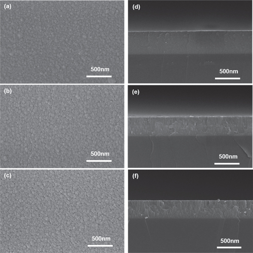
Figure shows the XRR data for the WO3 films at different Pchamber values on SiO2/Si substrates. Critical angles for the total reflection for the given films are known to be proportional to their electronic density and, consequently, their mass density. The WO3 film at Pchamber = 1.0 Pa had the highest mass density of 8.38 g/cm3. The mass density of the prepared WO3 films decreased as Pchamber condition increased. The lowest mass density of 5.72 g/cm3 was obtained for the WO3 film at Pchamber = 2.0 Pa, which is consistent with the SEM analysis (Figure ). This result can be explained by the concept of mean free path (λ) of ad-atoms during reactive sputtering. At the low Pchamber condition, ad-atom species such as WO, WO2, and WO3 are likely to be less scattered by the Ar atom or radical in the plasma chamber, leading to the enhanced λ and kinetic energy of ad-atoms near the growing surface. Thus, the energetic ad-atoms can migrate easily onto the growing surface and form a dense WO3 film. This is why the lowest Pchamber condition favors the formation of a smooth and dense micro-structure. However, the collision event between ad-atoms and Ar species will increase with increasing Pchamber, resulting in reduced λ and kinetic energy of ad-atoms. Consequently, a WO3 film with a rather porous and less dense random network is likely to form, resulting in rough morphology and smaller mass density in the SEM and XRR analysis [Citation36]. In general, the cell performance of ECDs with the WO3 EC layer is affected by various microstructural factors, such as porosity [Citation37], surface roughness [Citation38,Citation39], specific surface area [Citation40], electrical conductivity [Citation41], and crystallinity [Citation42]. Obviously, the kinetics of the ion diffusion, insertion/extraction, and charge transfer should impact the coloring/bleaching process. In this regard, novel approaches including increasing the contact area between WO3 film and electrolyte, enhancing the electrical conductivity of films, and designing specific nanostructures have been investigated [Citation37–42]. Here, the WO3 film with rough morphology and porous open network structure was obtained by carefully controlling Pchamber = 2.0 Pa, which can provide more reactive sites and shorter ionic diffusional path leading to better ion diffusion or insertion/extraction. Thus, it is anticipated that the WO3 film with the smallest mass density and roughest morphology can facilitate a fast and efficient coloring process because the possible existence of nano- or micro-scale pores or path assists Li+ diffusion [Citation43].
Figure 6. Measured XRR data for the WO3 films on the SiO2/Si substrate under different Pchamber conditions of 1.0, 1.5 and 2.0 Pa. Inset shows an enlarged graph of the XRR spectra.
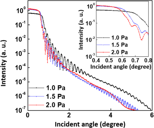
Figure (a)–(c) show the W 4f XP spectra for the WO3 films at different Pchamber conditions of 1.0, 1.5, and 2.0 Pa, respectively. Two strong sub-peaks at the binding energy of 35.8 and 38.0 eV can be assigned to W 4f7/2 and W 4f5/2 of W6+, corresponding to the stoichiometric WO3. In contrast, two smaller sub-peaks at 34.1 and 36.3 eV indicate the existence of W5+, which comes from the oxygen-deficient WO3-x. Interestingly, the fraction of stoichiometric WO3 went up with increasing Pchamber as shown in Figure (d). The role of VO in the oxygen-deficient WO3-x can be assessed by the optical transparency. The WO3 film at Pchamber = 1.0 Pa appeared as dark blue to the naked eye whereas the WO3 film at Pchamber = 2.0 Pa had a high transparency to visible light (see Figure S4). The Pchamber dependence on the non-stoichiometry during sputtering can be explained by the atomic mass disparity between W and O atoms [Citation44]. The occupied O 2p and the vacant W 5d0 in WO3 constitute the valence band maximum and conduction band minimum, respectively, which is responsible for the photochromic transition [Citation45]. The stoichiometric WO3 is a colorless transparent insulator. The dark blue color of the WO3 film at Pchamber = 1.0 Pa is attributed to the pre-existence of considerable W5+ ionic states. The coloration efficiency can be degraded further because the VO in non-stoichiometric WO3 hinder the chemical conversion from W+5 to W6+ upon the Li removal.
Figure 7. XPS spectra of W 4f for the films deposited at (a) 1.0 Pa, (b) 1.5 Pa, (c) 2.0 Pa, and (d) the O/W ratio as a function of sputtering pressure.
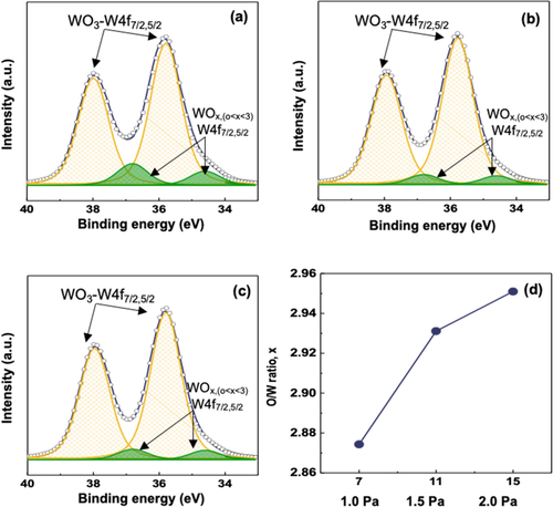
Figure (a)–(c) shows the CV characteristics of ECDs with the WO3 EC layer prepared under different Pchamber conditions. The dolphin-shaped area was smallest for the ECD with the WO3 EC layer at Pchamber = 1.0 Pa (Figure (a)). The largest dolphin-shaped area was observed for the device with a WO3 EC layer at Pchamber = 2.0 Pa. The influence of Pchamber on the ECD cell performance underscores the importance of microstructure in the WO3 EC layer. The coloration and bleaching process in the WO3 EC layer can be described using the following chemical equation:
(2)
(2)
Figure 8. (a)–(c) Cyclic voltammograms and (d)–(f) corresponding results on optical transmittance results.
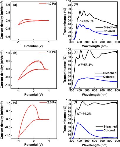
Here, Li+ is an ion in the lithium perchlorate electrolyte. The injection (extraction) of electrons and Li+ ions from the electrolyte causes coloration (bleaching) processes in the WO3 film [Citation46]. When a negative voltage is applied to the BE, the J value increases negatively with increasing cathodic potential, corresponding to the co-injection of e- and Li+ into WO3 to form tungsten bronzes. Anodic peaks occurring during the positive-bias sweep indicate the extraction of e- and Li+ from LixWO3 to the electrolyte. Reversible switching between the colored and bleached states requires Li+ charging and discharging through the EC layer. Obviously, the better coloration capability of the ECD with the WO3 EC layer at Pchamber = 2.0 Pa should be attributed to the porous and less dense random network nature of the WO3 film (XRR data) because the porous and open structure provides an efficient percolation diffusional pathway for the charge carriers such as e- and Li+. Figure (d)–(f) show the optical transmittance spectra of ECDs with different WO3 EC layers in the colored and bleached states under sweep voltages of ±1.0 V after 10-time cycle loading. As expected, the optical modulation range of ECDs was improved using the WO3 EC layer prepared at higher Pchamber conditions. The optical modulation range for the given ECD cell increased from 35.6% (WO3 EC layer at the Pchamber = 1.0 Pa) to 86.2% for the WO3 EC layer at Pchamber = 2.0 Pa.
Figure (a) shows the relationship between optical density and wavelength. Coloration efficiency (CE,η) is defined as the ratio of change in optical density (ΔODλ) to the corresponding injected/ejected charge density (Qin) per unit area (A), which is described as follows:
(3)
(3)
(4)
(4)
(5)
(5)
(6)
(6)
Figure 9. (a) Variation in the optical density difference (ΔODλ) with respect to the wavelength. (b) Coloration efficiency of WO3 films at different P chamber conditions of 1.0, 1.5 and 2.0 Pa. (c) The current density corresponding to the process of the response time.
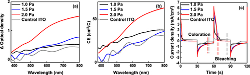
Here, Tbλ and Tcλ stand for the transmittance of bleached and colored samples, respectively. Using these formulas, the CE,η values for the ECDs with a WO3 EC layer at Pchamber = 1.0, 1.5 and 2.0 Pa were calculated at 35.7, 37.6, and 67.1 cm2C−1, respectively (Figure (b)). The ECD cell with the WO3 EC layer at the Pchamber = 2.0 Pa exhibits the best CE,η value (67.1 cm2C−1). Considering that CE,η values of 33.8 and 28.0 cm2C−1 were reported in the WO3 EC layer prepared by RF magnetron sputtering and spray pyrolysis, respectively, our approach involving the IAI stack as a TCO and porous WO3 as an EC layer using sputtering technique shows considerable promise. The switching time from the coloration to bleaching (or vice-versa) is also an important metric in the practical implementation of ECD. Figure (c) shows J versus time during the coloration and bleaching process using the CA method. The ECD with the WO3 EC layer at Pchamber = 1.0 Pa suffered from a slow response time (∼20 s) during the bleaching process due to the sluggish transport of Li+ and e- through the dense WO3 film. The improvement in terms of response time (∼5.7 s) during the bleaching process was achieved for the device with a WO3 EC layer at the Pchamber = 2.0 Pa, which is attributed to the lowest mass density WO3 film (Figure (c)).
Finally, it is noted that the performances of ECDs in this work are quite competitive compared to other studies regarding ECDs with WO3 EC materials (Table ). Though nanoparticle or nanowires-based approaches exhibited the highest CE (78.6∼132 cm2/C) owing to the nanoscale tailoring structure, the rather slower response time and complicated fabrication routes need to be resolved [Citation25, Citation47, Citation50, Citation51]. The good ΔT of 86.2% at the wavelength of 600 nm, relatively faster response time (Tc/Tb = 16/5.7 s) as well as the reasonable CE,η of 67.1 cm2/C for the given ECDs were achieved by tailoring the microstructure of the sputtered WO3 EC layer in conjunction with the TCO stack of IAI, which has mass production compatibility.
Table 3. Device performance comparisons of ECDs with WO3-based EC materials.
4. Conclusion
The feasibility of an IAI multi-layer stack was examined as a TCO for high-performance ECDs. The thickness-dependence of the structural and electrical properties of Ag films on the inserted ITO/SiO2/Si substrate was examined. We found that a 15 nm-thick Ag film characterized by the cubic Ag phase with a preferential orientation of (111) and smooth morphology was optimal. The IAI stack with the 15 nm-thick Ag film exhibited the highest FOM of 22.4 (RS of 16.6 Ω/cm2 and optical transmittance of 90.6%), which is suitable as TCO electrode for high-performance ECDs. Furthermore, the WO3 films with different mass densities were sputtered by controlling the Pchamber value during film preparation. As the Pchamber value increased, the prepared WO3 film showed decreasing mass density. Specifically, it decreased from 8.38 g/cm3 (Pchamber = 1.0 Pa) to 5.72 g/cm3 for the WO3 film at Pchamber = 2.0 Pa. The responsible growth model was discussed using the λ concept and kinetic energy of ad-atoms near the growing surface. The half-cell ECD with the IAI BE and porous WO3 EC layer exhibited the best coloration efficiency and improved response time, which can be attributed to (i) high FOM of the IAI stack and (ii) enhanced transport capability of Li ions (e-) through the open structural network of WO3. We concluded that the implementation of IAI stack and porous WO3 EC is an effective approach to producing high-efficiency ECDs.
Supplemental Material
Download MS Word (247.2 KB)Disclosure statement
No potential conflict of interest was reported by the author(s).
Additional information
Funding
Notes on contributors

Sueon Lee
Sueon Lee received his B.S. and M.S degrees in electronic engineering from Hanbat University, Daejeon, Republic of Korea in 2018, and her Ph.D. degree in electronic engineering from Hanyang University, Seoul, Republic of Korea in 2022. She is currently working at the LG Display Co., Ltd., South Korea, as a senior research engineer. Her research interest involves high-performance TFTs and advanced oxide materials with high mobility and reliability.

Min Jae Kim
Min Jae Kim received his B.S. degree in electronic engineering from Hanyang University, Seoul, Republic of Korea in 2017. He is currently in the M.S and Ph.D integration course of Electronics and Computer Engineering in Hanyang University, Seoul, Republic of Korea. His research interest involves the high performance and reliability of transition metal oxide semiconductor devices.

Sang Ho Lee
Sang Ho Lee received his B.S., M.S. degrees in Metallurgical Engineering from INHA University, Incheon, Korea in 1998 and 2001, respectively, and his Ph.D. degrees in Advanced Materials & Chemical Engineering from Hanyang University in 2015. He has worked on developing the sputtering equipment and process for flat panel display, electronic devices, and semiconductor since 2001. He is currently working as a general manager at Korea Institute for Super Materials, ULVAC KOREA Ltd.

Seung Hye Jeong
Seung Hye Jeong received her B.S. degree in engineering from Hallym University, Chuncheon, Republic of Korea in 2019, and her M.S. engineering degree from Kyung Hee University, Seoul, Republic of Korea in 2021. She is currently working at the Centmmaterials Co., Ltd., South Korea, as a senior research engineer. Her research interest involves high-performance and long-lifetime Organic Light Emitting Diodes.

Jang Hyuk Kwon
Jang Hyuk Kwon is a professor in the Department of Information Display at Kyung Hee University, South Korea. He received his Ph.D. degree in Chemistry from Korea Advanced Institute of Science and Technology (KAIST) in South Korea in 1993. Before joining Kyung Hee University, he was a Chief Researcher at Samsung SDI (South Korea) from 1993-2005. His research interests include the development of new organic materials for optoelectronic devices including OLEDs, QD-LEDs, OPV, and electrochromic devices. He has authored/co-authored over 150 SCI-indexed papers and also has over 100 registered patents (national and international) under his name.

Jae Kyeong Jeong
Jae Kyeong Jeong received his B.S., M.S., and Ph.D. degrees in material science and engineering from Seoul National University, Seoul, Korea, in 1997, 1999, and 2002, respectively. In 2003, he was a post-doctoral researcher at the University of Illinois at Urbana-Champaign. He joined Samsung Display Corp. as a senior engineer in 2004, where he performed research on the design and characterization of LTPS and IGZO TFTs for AMOLED display. In 2009, he joined Inha University as an assistant professor. Since September 2015, he has been with the Department of Electronic Engineering at Hanyang University, Seoul, Republic of Korea as a professor. He has more than 185 authored (or co-authored) international journal papers and 112 international patents under his name.
References
- P. Yang, P. Sun, and W. Mani, Mater. Today 19, 394 (2016).
- G.A. Niklasson, and C.G. Granqvist, J. Mater. Chem. 17, 127 (2006).
- D. Ma, J. Wang, H. Wei, and Z. Guo, John Wiley & Sons, Ltd 23 (2018).
- K.P. Sibin, G. Srinivas, H.D. Shashikala, A. Dey, N. Sridhara, and K. Sharma, Sol. Energy Mater. Sol. 172, 277 (2017).
- H. Ferhati, F. Djeffal, and A. Benhaya, Superlatt. Microst. 129, 176 (2019).
- H. Taha, Z.-T. Jiang, C.-Y. Yin, D.J. Henry, X. Zhao, and G. Trotter, J. Phys. Chem. C. 122, 3014 (2018).
- S.Y. Lee, Y.S. Park, and T.-Y. Seong, J. Alloys Compd. 776, 960 (2019).
- D.R. Sahu, S.Y. Lin, and J.L. Huang, Appl. Surf. Sci 252, 7509 (2006).
- D.R. Sahu, and J.L. Huang, Thin Solid Films 515, 876 (2006).
- D. Kim, Appl. Surf. Sci. 256, 1774 (2010).
- J.A. Jeong, Y. Park, and H.K. Kim, J. Appl. Phys. 107, 023111 (2010).
- L. Gong, L. Lu, and Z. Ye, Sol. Energy Mater. 95, 1826 (2011).
- K.H. Choi, H.J. Nam, J.A. Jeong, S.W. Cho, H.K. Kim, J.W. Kang, D.G. Kim, and W.J. Cho, Appl. Phys. Lett. 92, 223302 (2008).
- D.R. Sahu, and J.L. Huang, Appl. Surf. Sci. 253, 915 (2006).
- Y.S. Jung, Y.S. Park, K.H. Kim, and W.J. Lee, Trans. Electr. Electron. Mater. 14, 9 (2013).
- Y.Y. Choi, K.H. Choi, H. Lee, H. Lee, J.W. Kang, and H.K. Kim, Sol. Energy Mater. 95, 1615 (2011).
- S.-M. Lee, H.-W. Koo, T.-W. Kim, and H.-K. Kim, Surf. Coating. Technol. 343, 115 (2018).
- W. Ji, T. Wang, B. Zhu, H. Zhang, R. Wang, and D. Zhang, J. Mater. Chem C 5, 4543 (2017).
- J.H. Kim, T.-W. Kang, S.-N. Kwon, S.-I. Na, Y.-Z. Yoo, and H.-S. Im, J. Electron. Mater. 46, 306 (2017).
- S.-H. Park, S.-J. Lee, J.H. Lee, J. Kal, J. Hahn, and H.-K. Kim, Org. Electron. 30, 112 (2016).
- M. Acosta, J. Mendez- Gamboa, I. Riech, C. Acosta, and M. Zambrano, Superlatt. Microst. 127, 49 (2019).
- D.-Y. Cho, Y.-H. Shin, H.-K. Kim, Y.-J. Noh, S.-I. Na, and K.-B. Chung, J. Vac. Sci. Technol. 22, 021501 (2014).
- O. Arutanti, D.B.A. Nandiyanto, T. Ogi, O.T. Kim, and K. Okuyama, ACS Appl. Mater. 7, 3009 (2015).
- Y. Li, D. Chen, and A.R. Caruso, J. Mater. Chem. C 4, 10500 (2016).
- G. Cai, P. Darmawan, M. Cui, J. Chen, X. Wang, A.L.-S. Eh, S. Magdassi, and P.S. Lee, Nanoscale 8, 348 (2016).
- J. Zhang, L.X. Wang, H.X. Xia, D.C. Gu, and P.J. Tu, Sol. Energy Mater. 95, 2107 (2011).
- H. Zhang, G. Duan, G. Liu, Y. Li, X. Xu, Z. Dai, J. Wang, and W. Cai, Nanoscale 5, 2460 (2013).
- T. Brezesinski, F.D. Rohlfing, S. Sallard, M. Antonietti, and B. Smarsly, Small 2, 1203 (2006).
- R. Mukherjee, and P.P. Sahay, J. Alloys Compd. 660, 336 (2016).
- L. Yang, D. Ge, J. Zhao, Y. Ding, X. Kong, and Y. Li, Sol. Energy Mater. Sol. Cells 100, 251 (2012).
- X. Yang, P. Gao, Z. Yang, J. Zhu, F. Huang, and J. Ye, Sci. Rep. 7, 44576 (2017).
- X. Tan, D. Zhu, Z. Shi, and X. Zhang, Ceram. Int. 46, 13925 (2020).
- A.K. Isiyaku, A.H. Ali, and N. Nayan, Beilst. J. Nanotechnol. 11, 695 (2020).
- T.-H. Kim, S.-H. Park, D.-H. Kim, Y.-C. Nah, and H.-K. Kim, Sol. Energy Mater. Sol. Cells 160, 203 (2017).
- G. Haacke, J. Appl. Phys. 47, 4086 (1976).
- B.L. Zhu, J. Wang, S.J. Zhu, J. Wu, D.W. Zeng, and C.S. Xie, Thin Solid Films 520, 6963 (2012).
- A. Hasani, Q. Van Le, T.P. Nguyen, K.S. Choi, W. Sohn, H.W. Jang, and S.Y. Kim, Electrochrom. Acta 283, 1195 (2018).
- Y. Yin, T. Gao, Q. Xu, G. Cao, Q. Chen, H. Zhu, C. Lan, and C. Li, J. Mater. Chem. A 8, 9927 (2020).
- S. Poongodi, P.S. Kumar, D. Mangalaraj, N. Ponpandian, P. Meena, Y. Masuda, and C. Lee, J. Alloys Compd. 719, 71 (2017).
- L. Zhao, X. Huang, G. Lin, Y. Peng, J. Chao, L. Yi, X. Huang, C. Li, and W. Liao, Chem. Eng. J. 420, 129871 (2021).
- J. Kim, A.I. Inamdar, Y. Jo, S. Cho, A.T. Aqueel Ahmed, B. Hou, S. Cha, T.G. Kim, H. Kim, and H. Im, J. Mater. Chem. A 8, 13459 (2020).
- K. Tang, Y. Zhang, Y. Shi, J. Cui, X. Shu, Y. Wang, Y. Qin, J. Liu, H.H. Tan, and Y. Wu, Appl. Surf. Sci. 498, 143796 (2019).
- Q. Liu, Q. Chen, Q. Zhang, G. Dong, X. Zhong, Y. Xiao, M.-P.D. Ogletree, F. Reniers, and X. Diao, Electrochim. Acta 269, 617 (2018).
- M. Acosta, D. Gonzalez, and I. Riech, Thin Solid Films 517, 5442 (2009).
- G. Ki, H.J. Cho, Y.-M. Sheu, and H. Ohta, J. Phys. Chem. C 123, 15419 (2019).
- P.-W. Chen, C.-T. Chang, T.-F. Ko, S.-C. Hsu, K.-D. Li, and J.-Y. Wu, Sci. Rep. 10, 8430 (2020).
- D. Qiu, H. Ji, X. Zhang, H. Zhang, H. Cao, G. Chen, T. Tian, Z. Chen, X. Guo, L. Liang, J. Gao, and F. Zhige, Inorg. Chem. 58, 2089 (2019).
- T. Hao, S. Wang, H. Xu, X. Zhang, J. Xue, S. Liu, Y. Song, Y. Li, and J. Zhao, Chem. Eng. J. 426, 130840 (2021).
- A. Azam, J. Kim, J. Park, T.G. Novak, A.P. Tiwari, S.H. Song, B. Kim, and S. Jeon, Nano Lett. 18, 5645 (2018).
- X. Huo, H. Zhang, W. Shen, X. Miao, M. Zhang, and M. Guo, J. Mater. Chem. A 7, 16867 (2019).
- H. Gu, C. Guo, S. Zhang, L. Bi, T. Li, T. Sun, and S. Liu, ACS Nano 12, 559 (2018).