
Abstract
Semiconductors processed at low temperature for complementary metal–oxide semiconductors (CMOS) devices are receiving considerable attention in the field of integrated electronic applications. In this work, we demonstrated a CMOS inverter constructed by n-type ZnON and p-type Te TFTs where all the processes have been done at low temperature. The electrical measurements of proposed TFTs exhibit high mobility (> 100 and > 3 cm2/Vs in case of ZnON and Te TFTs, respectively) and a stable on/off current ratio. The resulted CMOS inverter exhibits a high voltage swing and a high voltage gain of 15.89. Since all the synthesis and fabrication processes are performed at low temperatures with easy processing techniques, the results may open new opportunities in the field of integrated electronics field.
1. Introduction
Low temperature processed semiconductors are highly preferred for large-area electronic devices such as complementary metal–oxide-semiconductor (CMOS) combination circuits, diode-based circuits, and logic circuits[Citation1, Citation2]. In particular, amorphous oxide semiconductors (AOS) such as indium gallium zinc oxide (IGZO) [Citation3], silicon indium zinc oxide (SIZO) [Citation4], and zinc tin oxide (ZTO) [Citation5] are promising candidates for n-type high-performance thin-film transistors (TFTs) with good electrical performances in terms of electron mobility, on/off ratio and current density. However, they are still limited in obtaining high carrier mobility at low-temperature, light-stressed stability, and stable transport measurements. In this regard, zinc oxynitride (ZnON) has previously been reported as a promising candidate for stable transport measurements and high carrier mobility [Citation6], but obtaining easy processing steps, high integration, and low-cost manufacturing still requires considerable work and attention.
Regarding microelectronic CMOS circuits, various p-type semiconductors materials such as carbon nanotubes (CNTs) [Citation7], pentacene [Citation8], and Dinaphthothienothiophene (DNTT) [Citation9] have recently been reported to form hybrid combinations of complementary circuits with n-type AOS. These combinations provide good electrical performance but are limited in terms of easy processing, high integration compatibility, large-scale processing, and low process temperature characteristics. Among various p-type semiconductors, tellurium (Te) has gained tremendous attention with its easy processing techniques, high uniformity, and good electrical performance [Citation10–12]. In particular, Te-based thin-film transistors have successfully been demonstrated in photo-sensing devices and large-scale integrations [Citation10–12], but they are still limited in terms of high-level integration and applicability in the field of electronics.
Here, we demonstrate a hybrid integration of n-type Zn-ON and p-type Te TFTs to achieve high CMOS inverter properties that show potential as replacement for conventional CMOS technology. The low-temperature sputter processed n-type Zn-ON-based TFT exhibits a high field-effect mobility value of 106.17 cm2/Vs along with excellent output properties, revealing highly stable saturation IDS at high VDS. The p-type Te semiconductor material was deposited using a direct current (DC) sputtering technique at low temperature (<25°C) without any additional annealing treatment. The Te-based TFT resulted in mobility of 4.35 cm2/Vs along with stable output properties. The complementary configurations of Zn-ON and Te TFTs were integrated to fabricate the CMOS inverter. The results exhibit a high gain of 15.89 and stable electrical performances, offering new opportunities in designing logic circuits based on hybrid semiconductor materials.
2. Results and discussion
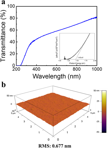
To obtain high electrical performance and uniform distribution of ZnON film, a radio frequency (RF) sputtering process was utilized to deposit the ZnON film where the applied RF power was fixed at 40 W and plasma gas flow of Ar:O2:N2 was 5:0.1:20 sccm. UV-vis spectrometer analysis was performed to confirm the optical properties of ZnON film. Figure a shows the transmittance of ZnON film from 200 nm to 1000 nm wavelength with the ZnON film showing a transmittance of over 55% at a wavelength of 550 nm. The inset image of Figure a shows the extracted optical bandgap of 1.45 eV using the Tauc method. ZnON film shows the smooth surface of RMS 0.677 nm, confirmed with atomic force microscope (AFM), as shown in Figure b.
Figure 1. (a) Optical transmittance of ZnON film. The inset graph shows the extracted optical band gap. (b) AFM image of ZnON with a scan size of 5 × 5 um.
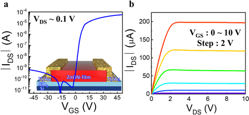
Next, the ZnON TFTs were fabricated on highly doped p-type Si substrates with a thermally grown 100 nm thick SiO2 using a simple shadow mask technique. The final width and length of devices were 800 and 200 um, respectively. The electrical properties of ZnON TFTs are depicted in Figure a and b. In transfer curves, the drain voltage was fixed at 0.1 V, while the sweep range of gate voltage was from −50 to 50 V (Figure (a)). ZnON TFT exhibits field-effect mobility, threshold voltage, and SS value of 110.26 cm2/Vs, 3.25 V, and 1.12 V/dec, respectively. Output curves were obtained where the drain voltage ranges from 0 to 20 V and gate voltage ranges from 0 to 10 V in the steps of 2 V (Figure (b)). The output curves show a clear pinch-off and no current crowding.
Figure 2. (a) Transfer and (b) Output curves of the proposed ZnON TFTs.
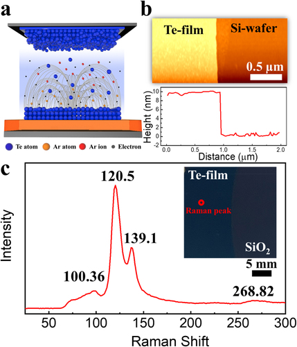
Driven by the potential applications for complementary configurations, a uniform Te-film is deposited through DC sputtering process at low temperature (<25°C) in the presence of argon (Ar) gas flow on SiO2/Si substrate, as shown in the 3D layout of Figure a. The thickness (∼10 nm) of the Te-film is confirmed by using AFM, revealing highly uniform film deposition as shown in Figure b in terms of microscopy image (upside) and graphical representation (downside). A clear view of Te-film and Si wafer is also shown. To understand the Te-film quality and van der Waals interactions, Raman spectroscopy is measured on the Te sample under an excitation wavelength of 532 nm, showing the A1 peak at 120.5 (cm−1), E2 peak at 139.1 (cm−1) as shown in Figure c, revealing the presence of high quality and uniform Te-film. Moreover, the inset of Figure c reveals the clear optical view for distinguishing Te-film and SiO2 wafer, demonstrating high uniformity of the sputtered Te-film.
Figure 3. (a) A 3D layout of the proposed sputtering process for uniform Te-film deposition at low temperature in the presence of Ar gas flow. (b) Thickness profiles of the proposed Te-film in terms of AFM image (upside) and height profile (downside). (c) Raman spectroscopy of the deposited Te-film with an inset of Te-substrate and marking of Raman measurement point.
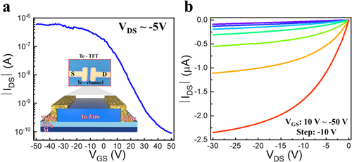
After the synthesis of uniform Te-film, the Te-based TFT is fabricated using a simple shadow mask technique. The transistor characteristics are then measured in terms of transfer and output curves, as shown in Figure a and b, respectively. The fabricated Te-TFT is shown in the inset of Figure a in terms of schematic layout and real image. The transfer properties (VGS – IDS) of the proposed Te-TFT reveal a smooth p-type curve with an Ion/Ioff of ∼104 and a threshold of 15.5 V at VDS of −5 V (Figure (a)). The proposed Te-TFT exhibits carrier mobility of 3.45 cm2V−1s−1 by using the formula µeff = Lgm/WCoxVDS, where L/W represents the channel length/width of 30/50 µm, gm represents the transconductance, VDS represents the drain voltage and Cox represents the capacitance of the oxide dielectric layer. The output properties (VDS – IDS) show a linear response at high VDS value and saturate current response at low VDS value at various VGS levels in the range of 10 V ∼ −50 V with a step of −10 V, as shown in Figure b.
Figure 4. (a) Transfer curve of the fabricated Te-based TFT along with a schematic and real image of the TFT. (b) Output curve of the proposed Te-based TFT at VGS ranges from 10 V to −50 V with a step of −10 V.
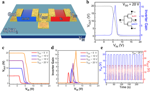
The combination of n-type ZnON and p-type Te TFTs enables the inverter device for CMOS application, shown in the 3D schematic layout of Figure a. The voltage transfer and gain curve of the proposed CMOS inverter is illustrated in Figure b. The applied voltage (VDD) was set to 20 V, while the input voltage (VIN) was set in the range of −5 V to 20 V, indicating the output characteristics of the CMOS inverter were in full-swing mode with an inverter gain of 15.89. Additionally, comparison of the proposed CMOS inverter with previous reports is demonstrated in the supplementary information (Table S1) to promote understanding of the advantages of the proposed CMOS inverter device. The voltage transfer characteristics were measured at different VDD ranges from 5 V to 20 V with a step of 5 V, revealing a full-swing mode as shown in Figure c. In addition, Figure d shows the inverter gain of the proposed CMOS inverter device in the range of 5.12–15.89. Here, the gain was extracted from the formula G = abs.dVOUT/dVIN. Next, the time-domain measurement of the CMOS inverter device was measured by applying the pulse of VIN of 20 V, while the output voltage (VOUT) was analyzed at VDD of 20 V as shown in Figure e. Results reveal the high stability and reliability of the inverter swing, consequently enabling low-temperature processed materials to be utilized in the integrated devices for next-generation electronic applications.
Figure 5. (a) A schematic layout of the hybrid Te and ZnON TFTs-based CMOS inverter device. (b) Transfer voltage and inverter gain curves of the proposed inverter device at VDD of 20 V with an inset of the schematic circuit layout. (c) and (d) Transfer voltage and inverter gain curves of the inverter device at different VDD range from 5 to 20 V with a step of 5 V. (e) Time-domain output curve measurements of the inverter device by applying VIN pulse of 20 V at VDD 20 V.
3. Conclusion
The integration of n-type ZnON and Te TFTs has been successfully fabricated at low-temperature for the CMOS inverter. The electrical properties of the proposed ZnON and Te TFTs exhibit high mobility of >100 cm2/Vs and >3 cm2/Vs, respectively, with high on/off current ratio. All the processes to synthesize the channel materials of ZnON and Te are performed at low temperature with uncomplicated processing techniques. The combination of ZnON and Te TFTs results in CMOS inverters with full-swing output properties and high inverter gain. With the advantages of low temperature and easy processing, the reported results may provide new opportunities for circuit designing in the field of integrated electronics.
Supplemental Material
Download MS Word (21.5 KB)Disclosure statement
No potential conflict of interest was reported by the author(s).
Additional information
Funding
Notes on contributors

Muhammad Naqi
Muhammad Naqi received his Ph.D. degree (2021) in Advanced Material Science and Engineering at Sungkyunkwan University (SKKU), Republic of Korea. His research interests include flexible/stretchable electronic sensors and devices, photodevices, memory/logic devices, artificial synaptic devices, and transition metal dichalcogenide-based thin-film transistors.

Seong Cheol Jang
Seong Cheol Jang received his B.S. and M.S. degrees (2021) from the Department of Material Science and Engineering of Chungnam National University (CNU), Republic of Korea. He is currently working towards a doctoral degree at CNU. He has been researching on oxide/nitride semiconductors, thin-film transistors (TFTs), polymer gate dielectrics, and flexible/stretchable devices.

Yongin Cho
Yongin Cho is currently working towards a master’s degree in Advanced Materials Science and Engineering from Sungkyunkwan University, Republic of Korea. His research interests include logic/neuromorphic devices based on large-area thin-film electronics.

Ji Min Park
Ji-Min Park is currently a Ph.D. student in the Department of Materials Science and Engineering at Chungnam National University (CNU) under the supervision of Prof. Hyun-Suk Kim. Her research interests include oxide/nitride semiconductors, bipolar semiconductors, thin-film transistors (TFTs), and neuromorphic devices.

Joo On Oh
Joo On Oh received his B.S. degree from the Department of Organic Material & Fiber Engineering of Soongsil University, South Korea in 2021. He is currently working on his Master’s degree in the Department of Advanced Materials Science and Engineering at Sungkyunkwan University. His current research interests include p-type transistors and logic devices.

Hyun Yeol Rho
Hyun Yeol Rho received his B.S. degree in nanomedical organic materials engineering from Yeungnam University, South Korea in 2018. He is currently working on his Master/Ph.D. degrees in the Department of Advanced Materials Science and Engineering at Sungkyunkwan University. His current research interests include p-type transistors and ferroelectric materials.

Hyun-Suk Kim
Prof. Hyun-Suk Kim received his Ph.D. from Korea Advanced Institute of Science and Technology (KAIST), Korea in 2006. After completing postdoctoral fellowship at the MIT, USA from 2007 to 2009, he joined the Samsung Advanced Institute of Technology as research staff member of the Display Devices Lab. In 2014, he moved to Chungnam National University, Republic of Korea as an assistant professor. He is currently a professor in the Department of Materials Science and Engineering at Chungnam National University. His current research interests are thin film transistors, MOSFET, CMOS device, all-solid-state battery, materials design & modeling, thin film coating technologies, and surface & interface analysis. He has published more than 130 SCI papers including work on Energy & Environmental Science, Advanced Materials, ACS Nano, Advanced Science and Nature.

Sunkook Kim
Sunkook Kim is an associate professor in the Department of Advanced Materials Science & Engineering at Sungkyunkwan University (SKKU). He received his Ph.D. in Electrical and Computer Engineering at Purdue University in 2009 and worked at Intel and Samsung Electronics until 2012. His research interests include the large-area synthesis of 2D materials, high-mobility thin-film transistors, wearable electronics, and human-digital interactive sensors. He received the Young Scientist Award from the Korean President in 2015 and the Display Challenger Award (Foldable OLED Display) from Samsung Electronics in 2010. He has authored and co-authored over 200 technical journal articles and conference papers.
References
- Z. Wang, H.A. Al-Jawhari, P.K. Nayak, J.A. Caraveo-Frescas, N. Wei, and M.N. Hedhili, Sci. Rep. 5, 1–6 (2015). doi:10.1038/srep09617.
- J.W. Park, B.H. Kang, and H.J. Kim, Adv. Funct. Mater. 30 (20), 1904632–40 (2020). doi:10.1002/adfm.201904632.
- J.-S. Kim, J.-H. Jang, Y.-D. Kim, J.-W. Byun, K. Han, J.-S. Park, and B.-D. Choi, IEEE Trans. Electron Devices 64 (10), 4123–4130 (2017). doi:10.1109/TED.2017.2738665.
- M. Naqi, J.Y. Lee, B.H. Lee, S. Kim, S.Y. Lee, and H. Yoo, IEEE J. Electron Devices Soc. 9 (no. 2021), 180–186 (2021). doi:10.1109/JEDS.2020.3048725.
- P. Schlupp, S. Vogt, H. Von Wenckstern, and M. Grundmann, APL Mater. 8 (6), (2020). doi:10.1063/1.5143217.
- H.-D. Kim, M. Naqi, S.C. Jang, J.-M. Park, Y.C. Park, K. Park, H.-H. Nahm, S. Kim, and H.-S. Kim, ACS Appl. Mater. Interfaces 14 (11), 13490–13498 (2022). doi:10.1021/acsami.1c24880.
- L. Ding, Z. Zhang, S. Liang, T. Pei, S. Wang, Y. Li, W. Zhou, J. Liu, and L.-M. Peng, Nat. Commun. 3 (2012). doi:10.1038/ncomms1682.
- I. Mejia, A.L. Salas-Villasenor, A. Avendano-Bolivar, J. Horvath, H. Stiegler, B.E. Gnade, and M.A. Quevedo-Lopez, IEEE Electron Device Lett. 32 (8), 1086–1088 (2011). doi:10.1109/LED.2011.2157801.
- K. Fukuda, T. Sekitani, T. Yokota, K. Kuribara, T.C. Huang, T. Sakurai, U. Zschieschang, H. Klauk, M. Ikeda, H. Kuwabara, and T. Yamamoto, IEEE Electron Device Lett. 32 (10), 1448–1450 (2011). doi:10.1109/LED.2011.2161747.
- M. Naqi, K.H. Choi, H. Yoo, S. Chae, B.J. Kim, S. Oh, J. Jeon, C. Wang, N. Liu, S. Kim, and J.-Y. Choi, NPG Asia Mater. 13 (1), (2021). doi:10.1038/s41427-021-00314-y.
- M. Naqi, K.H. Choi, Y. Cho, H.Y. Rho, H. Cho, P. Pujar, N. liu, H-S Kim, J-Y Choi, and S. Kim, Adv. Electron. Mater. 8, 2101331–10 (2022). doi:10.1002/aelm.202101331.
- C. Zhao, C. Tan, D.H. Lien, X. Song, M. Amani, M. Hettick, H.Y.Y. Nyein, Z. Yuan, L. Li, M.C. Scott, and A. Javey, Nat. Nanotech. 15 (1), 53–58 (2020). doi:10.1038/s41565-019-0585-9.