
Abstract
Area-selective atomic layer deposition (AS-ALD) has been studied as an alternative method for metal oxide ALD film patterning in the microelectronics industry. To perform AS-ALD, area-deactivation or -activation processes should be implemented in advance using selective surface modification through a photography-based lift-off process and printing techniques. This study introduces a novel approach for Al2O3 AS-ALD using inkjet-printed inhibition patterns. ALD-inhibition patterns with two-layer structures of fluorocarbon (FC) thin film and photoresist (PR) were patterned by inkjet printing. Low surface energy FC thin films were used to block the Al2O3 nucleation and growth during the ALD process, and PR was patterned to easily remove ALD-inhibition patterns using a lift-off process. To demonstrate AS-ALD, an Al2O3 thin film approximately 10 nm thick was deposited via an in-house built system with a multiple-slit gas source. The proposed AS-ALD method was evaluated for topological analysis using atomic force microscopy and surface composition analysis using a time of flight secondary ion mass spectrometry after Al2O3 deposition and a lift-off process. Finally, a 6 nm thick Al2O3 film was selectively patterned by the lift-off process using an inkjet-printed 1.28 μm thick FC-covered PR inhibition pattern.
1. Introduction
Atomic layer deposition (ALD) as a thin film deposition process is implemented by the alternate pulsing of precursor gases and surface reactions between vapors and reactive sites on the substrate [Citation1]. The formation of films is restricted to one atomic layer at a time because surface reactions in the ALD process occur only at reactive sites [Citation2]. Therefore, ALD enables the deposition of films with high material quality, good uniformity, high conformality, and accurate thickness control [Citation3,Citation4].
In the microelectronics industry, area-selective atomic layer deposition (AS-ALD) has recently attracted significant attention as an alternative method for metal oxide ALD [Citation5]. Since ALD depends on surface chemistry, AS-ALD can be achieved by selective chemical modification of the substrate surface, which is in turn achieved by a photography-based lift-off process as well as printing techniques for area-deactivation or -activation. Many research groups have studied the AS-ALD process to achieve metal oxide film patterns of Al2O3, HfO2, TiO2, and ZnO [Citation2,Citation4–9]. Self-assembled monolayers (SAMs) such as octadecylphosphonic acid (ODPA) and octadecyltrichlorosilane (ODTS) are used as ALD-blocking layers for selective prevention of nucleation and growth during ALD processes [Citation4,Citation6]. Some of the reported AS-ALD processes use unreactive and thermally stable polymer thin films made of poly (methyl methacrylate) (PMMA) and poly (vinyl pyrrolidone) (PVP) [Citation7,Citation9] as an ALD-blocking layer.
Al2O3 thin film is widely used as a functional material in the fabrication of various electronic and optoelectronic devices due to its high transparency and refractive index, thermal conductivity, good adhesion to various surfaces, thermal and chemical stability, and high dielectric constant [Citation10–12]. Some of its important applications include as gas diffusion barrier layer in the encapsulation of organic light-emitting diode devices [Citation13,Citation14], antireflection coating in solar cells [Citation15], and gate dielectric film in thin-film transistors [Citation16,Citation17]. However, very few studies have reported AS-ALD of Al2O3 using SAMs and polymer thin films or patterning processes constructed using O2 plasma and acid chemical etching on the metal oxide-coated surface [Citation6,Citation18]. Seo et al. studied ODPA as a SAM to block Al2O3 film, where they performed AS-ALD of Al2O3 only on the ODPA-coated Ti pattern formed by O2 plasma etching [Citation18]. It has been reported that selective patterning of Al2O3 grown using trimethylaluminum (TMA) and H2O for the Si surface is nearly impossible, even if hard mechanical scribing is used to remove Al2O3 from blocking layers such as PMMA, PVP, and plasma-polymerized fluorocarbon (FC) films [Citation19–22]. Most studies have used AlCl3 [Citation7,Citation20] or dimethylaluminum isopropoxide [Citation9,Citation23] as the aluminum precursor to demonstrate AS-ALD of Al2O3 without additional chemical etching of metal oxide surface.
Photolithography-based lift-off processes or microcontact printing are generally used to pattern SAMs for AS-ALD [Citation8,Citation23–26]. However, since a typical SAM is ∼2 nm thick, it is quite challenging to fabricate features thicker than a few nanometers [Citation5]. The increase in film thickness over the height of SAM during ALD leads to lateral film overgrowth [Citation3,Citation5]. Furthermore, it is important to form a defect-free SAM to effectively block the growth of films during ALD [Citation3]. It usually takes more than 24 h to obtain a well-packed SAM by immersion of the sample in solution or by vapor deposition [Citation27]. In the case of polymer films, spin coating and photolithography-based lift-off processes can be used to easily control the thickness of ALD-inhibition patterns and obtain thicker polymer films [Citation7,Citation9,Citation28]. The inkjet printing process was introduced as an alternative patterning method to pattern polymer thin films for AS-ALD [Citation9,Citation20]. This process was transformed into a sophisticated device manufacturing method for low-cost, large-area, and flexible electronics [Citation29]. One of the main advantages of this process is the ability to position the material on planar and non-planar substrates using computer control to produce structures without the need for photomasks [Citation30]. The inkjet printing process can control the thickness of the target materials at the desired position using an overprinting technique. By increasing the number of the inkjet head, various materials can be printed simultaneously and multi-layered patterns can be realized by layer–by–layer printing. The inkjet printing process is less time-consuming to form mask patterns for AS-ALD when compared to the film patterning methods of both SAMs and polymers.
To date, there has been no demonstration of AS-ALD using Al2O3 grown by TMA and H2O using inkjet-printed blocking layers on the Si surface. In this study, the inkjet printing process was utilized to form ALD-inhibition patterns with two-layered structures for the AS-ALD process. The ALD-inhibition pattern printing process was developed by using two techniques: overprinting for thickness control and multilayer printing, which are unique advantages of inkjet printing. Al2O3 was chosen as a model metal oxide for selective ALD due to its enormous potential in various fields. FC thin films were inkjet-printed to inhibit Al2O3 nucleation and growth during the ALD process. A thicker photoresist (PR) was inkjet-printed to allow easy removal of ALD-inhibition patterns using a lift-off process. FC, PR, and FC-covered PR (FC/PR) patterns were prepared as ALD-blocking test patterns on Si substrate by inkjet printing. To demonstrate AS-ALD, Al2O3 thin film was deposited via an in-house built system with a multiple-slit gas source. The Al2O3 ALD-inhibition performance of the prepared patterns was evaluated for topological analysis using atomic force microscopy (AFM), surface composition analysis using time of flight secondary ion mass spectrometry (TOF-SIMS) after the lift-off process by O2 plasma, and ultrasonic agitation.
2. Experimental details
An inkjet printer (DMP2800, Dimatix-Fujifilm Inc.) was used to print the patterns with FC and PR inks. The FC ink (mixture of FC40 and FC722, 3M) was printed to form a low surface energy pattern. FC 40 was used as a solvent, and FC722 as a solute to prepare FC ink. The PR ink was prepared by mixing commercial PR (DSAM-3020, Dongjin Semichem Co.) with ethyl lactate (EL) solvent. FC and PR inks were jetted using 1 and 10 pl cartridges (DMC-11610, Fujifilm Dimatix Inc.), respectively. Si wafer was used as the substrate.
We deposited the Al2O3 thin films via an in-house built roll-to-roll ALD system with a multiple-slit head for gas source supply. The growth rate is determined by the speed of the substrate that is continuously moving relative to the simultaneously delivered precursor sources. The substrate moving speed was maintained at 5 mm/sec. Al2O3 thin films were grown on the substrates at room temperature and under a working pressure of 750 Torr. A total gap of ∼250 μm was maintained between the multiple-slit head and the moving substrate. Both the multiple-slit head and substrate were heated to 100 °C.
TMA and H2O were used as precursors, which were delivered into the multi-slit head with nitrogen gas at flow rates of 700 and 1000 sccm, respectively. H2O was purged for 10 s. The growth rate of Al2O3 was ∼0.97 Å per cycle. To achieve ∼10 nm target thickness, Al2O3 was deposited on Si substrates with printed ALD blocking patterns [Citation31,Citation32].
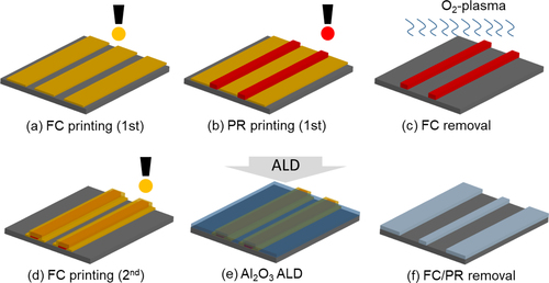
Figure shows a schematic diagram of the proposed AS-ALD method using the inkjet-printed ALD-inhibition test patterns and lift-off process. The procedure was as follows: (a) FC inkjet printing was used to define the PR pattern width by hydrophobic patterns; (b) PR was printed inside the gap of hydrophobic line patterns; (c) FC removal was performed using O2-plasma; (d) FC cover-layer was printed on the PR pattern; (e) Al2O3 ALD was conducted; (f) FC-covered PR inhibition pattern was removed by a lift-off process using an ultrasonicated acetone solution.
Figure 1. Schematic diagram of the proposed AS-ALD method using inkjet-printed ALD-inhibition test patterns and lift-off process.
The cross-sectional profile and topology of the printed patterns and the Al2O3 layer were analyzed using AFM (NX10, PARKSYSTEMS). Surface composition analysis was performed using TOF-SIMS (ION TOF, TOF.SIMS-5 equipped with a Bi source and sputter gun). The pressure for the TOF-SIMS and preparation chambers was maintained at 3.8 × 10⁻⁹ Torr. The Bi+ primary ions were accelerated at 30 keV and 0.5 nA current. A ∼90 nm diameter probe beam was rastered over a 150 μm × 150 μm area during data acquisition.
3. Results and discussion
To investigate the inhibition of Al2O3 film growth during the ALD process using the prepared ink materials, FC, PR, and FC-covered PR (FC/PR) patterns were fabricated on a Si substrate by inkjet printing. The layer structure is depicted in Figure . In our previous research [Citation33], we demonstrated AS-ALD using inkjet-printed FC patterns with low surface energy and O2 plasma. An experiment on droplet jetting stability, print-overlap rate, and substrate temperature was conducted to find the correct printing condition for forming a straight FC line pattern. An FC line pattern with a width of ∼40 μm was formed by printing FC dot patterns of ∼40 μm diameter with a print-overlap rate of 73% (print drop pitch = 29 μm) at a substrate temperature of 50°C [Citation33]. The printed FC patterns were heated at 110°C for 10 min in an oven. In this study, we also prepared 40 μm-wide FC stripe patterns at intervals of 10 μm on the Si substrate with the same ALD-inhibition pattern design. The FC thin film has a sufficiently low surface energy of 13.04 dynes/cm compared to that of other inhibitory layers such as ODPA, ODTS, PMMA, and PVP thin films, which acts as an inhibitor for AS-ALD [Citation4,Citation6,Citation7,Citation9].
The surface energy of FC thin films was calculated by the Owen–Wendt geometric mean model, and contact angles were measured via a sessile drop method using three probe liquids (CH3NO, CH2I2, H2O). The thickness of the FC pattern was about 3 nm at its middle region, while the borderline height of the FC mask line pattern was ∼8 nm owing to the coffee–ring effect [Citation33].
The ink-jetting characteristic of the diluted PR solution for PR printing was evaluated by changing the EL-mixing ratio. Table shows the viscosity, surface tension, and ink-jetting performance for the various mixing ratios of the PR and EL solvents. Undiluted PR of 25 cP was not ink-jetted, but it was possible to ink-jet the mixture of PR and EL at mixing ratios of 33 and 50% v/v, resulting in a viscosity of 7.5 cP or less. Figure (a–d) shows the PR dot patterns inkjet-printed with a single drop in the hydrophilic tracks. First, the hydrophobic FC ink was printed with the desired gap distance to form a hydrophilic track. In this step, the width of the PR pattern was decided by the width of the hydrophilic track (Wtrack) between the FC line patterns [Citation34]. The hydrophilic track width decreased at 10-μm intervals from 60 to 30 μm. Lengths of the PR dot patterns in the hydrophilic track were measured and found to be 69, 73, 85, and 96 μm, depending on the hydrophilic track width. Thereafter, to form the PR straight line using the process depicted in Figure (a-b), PR ink was continuously printed with a print-overlap rate of 30% of each dot length, as shown in Figure . The center thickness of the line pattern increased from 0.1–0.5 μm, as the line width decreased from 60 to 30 μm, as shown in the cross-sectional profile analysis in Figure (e). In addition, the coffee–ring effect decreased as the line width of the PR pattern decreased, and its thickness increased. For better understanding, the region of the FC line pattern is indicated by a dotted line in Figure (a) and Figures (a), and FC line patterns exist on both side regions of the PR patterns. After dipping in water, it was possible to discriminate FC patterns with the help of water spots formed on the non-wettable FC patterns (image not shown). Because the printed FC pattern is transparent, it was hard to directly discriminate the patterns in optical microscopic images.
Figure 2. PR dot patterns inkjet-printed with a single drop on hydrophilic tracks: (a) Wtrack = 60 µm, (b) Wtrack = 50 µm, (c) Wtrack = 40 µm, (d) Wtrack = 30 µm (Wtrack = hydrophilic track width between FC line patterns).
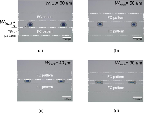
Figure 3. Inkjet-printed PR line patterns on hydrophilic tracks (Wtrack): (a) Wtrack = 60 µm; (b) Wtrack = 50 µm; (c) Wtrack = 40 µm; (d) Wtrack = 30 µm; (e) cross-sectional profile (Wtrack = a hydrophilic track width between FC line patterns).
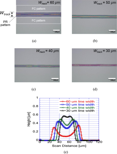
Table 1. Ink-jetting performance for mixing ratios of PR and EL solvents.
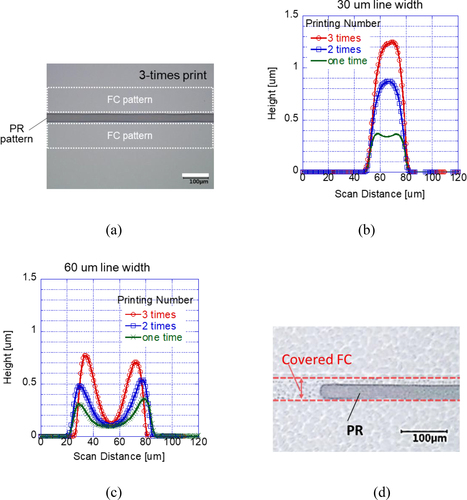
To increase the thickness of the PR patterns, these were overprinted in the hydrophilic track using the layer–by–layer printing method. Overprinting was performed by a solvent drying process between inkjet printing passes. After overprinting three times while maintaining the line width pre-defined by both hydrophobic FC patterns, straight PR patterns remained well-defined without the bulging phenomenon (Figure (a)) [Citation35]. The thickness of the 30 μm width PR line pattern increased from 0.45–1.28 μm depending on the print number (from 1 to 3), without the coffee–ring effect as shown in the cross-sectional profile analysis in Figure (b). However, in the case of 40, 50, and 60 μm line widths, the coffee–ring effect was observed on the edge of the printed PR line pattern despite increasing the print number. In particular, for the 60 μm line width, the center thickness was almost unchanged at about 0.1 μm and the height of both side edges increased from ∼0.3 to ∼0.8 μm (Figure (c)). Finally, FC/PR patterns (Figure (d)) were fabricated by printing FC ink onto PR patterns as a cover layer according to the process shown in Figure (a–d).
Figure 4. PR patterns overprinted on hydrophilic tracks using layer–by–layer printing method: (a) optical microscopic image of 3-times printed PR pattern, (b) cross-sectional profile of 30 μm line width, (c) cross-section profile of 60 μm line width, (d) optical microscopic image of FC/PR pattern.
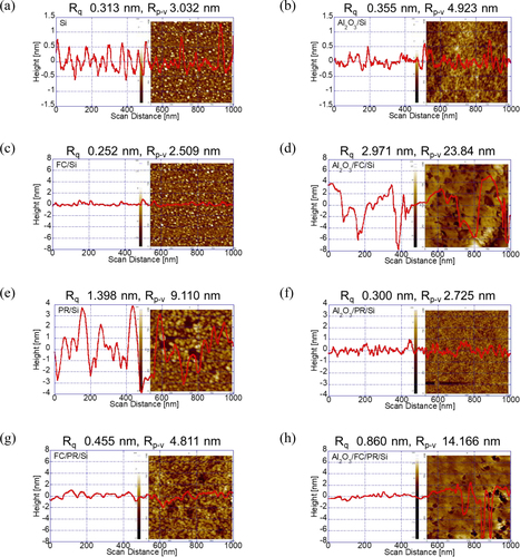
To demonstrate AS-ALD, Al2O3 thin films approximately 10 nm thick were deposited on the inkjet-printed FC, PR, and FC/PR ALD-inhibition patterns on the Si substrate by inkjet printing. Figure shows the AFM analysis results for a 1 μm × 1 μm scanned area before and after Al2O3 ALD on various surfaces. The root mean square roughness (Rq) of Al2O3-deposited Si substrate increased to 0.355 nm (Figure (b)) compared to that of bare Si surface, 0.313 nm (Figure (a)). Peak–to–valley roughness (Rp–v) of Al2O3-deposited Si substrate increased from 3.032 nm to 4.923 nm after the ALD process. For the FC surface, Rp–v remarkably increased from 2.509 (Figure (c)) to 23.84 nm (Figure (d)). Unlike the Al2O3-deposited Si surface, many cavities were irregularly distributed on the lumped and undulated Al2O3-deposited FC surface. Fine grains appeared on the Al2O3 deposited PR surface, as shown in Figure (e, f). Rq decreased from 1.398–0.300 nm, and Rp–v decreased from 9.110–2.725 nm after Al2O3 deposition. For the FC film-covered PR surface, Rq abruptly increased from 0.455 (Figure (g)) to 0.860 nm (Figure (h)). Cavities were observed on the lumped and undulating surface, similar to the Al2O3-deposited FC surface. To summarize the AFM analysis, all surfaces before Al2O3 deposition showed fine-grain spreading topology. Al2O3 deposition showed a tendency to increase Rq and decrease Rp–v. In the case of the Si and PR surfaces, surface morphology maintained a fine-grain spreading topology even after Al2O3 deposition. However, FC and FC film-covered PR showed lumped and undulating surfaces, including cavities, along with an abrupt increase of Rq.
Figure 5. Results of AFM analysis on 1 μm × 1 μm scanned area before and after Al2O3 ALD on various surfaces: (a) bare Si; (b) Al2O3-deposited Si surface; (c) FC-coated Si (FC/Si) surface; (d) Al2O3-deposited FC/Si surface; (e) PR-coated Si (PR/Si) surface; (f) Al2O3-deposited PR/Si surface; (g) FC-covered PR/Si (FC/PR/Si) surface; (h) Al2O3-deposited FC/PR/Si surface.
After Al2O3 ALD on the prepared lift-off patterns, we tried to remove unwanted regions using O2 plasma or ultrasonic agitation. First, in the experiment for AS-ALD of Al2O3 using FC patterns, removing the unwanted FC patterns with 10 min of O2 plasma treatment was possible as reported in the previous study. Finally, a 10 μm wide and 6 nm thick Al2O3 pattern was formed on the Si substrate (Figure (b)) [Citation33]. In this study, TOF-SIMS analysis was carried out to map residual element information before and after lift-off patterning of Al2O3 thin film and to investigate the inhibition properties of FC patterns during the Al2O3 ALD process. As shown in Figures (c) and (d), there was no signal of AlO- before Al2O3 thin film deposition on Si substrate with FC pattern. Although Al2O3 was physically patterned by O2 plasma as shown in Figure (b), AlO– was detected in the two-dimensional TOF-SIMS mapping images after Al2O3 deposition and lift-off patterning (Figure (e)). Also, AlO– was detected by depth profile analysis underneath the background blocked by the FC lift-off patterns. This means that FC lift-off patterns could not entirely inhibit Al2O3 growth. Al2O3 thickness was estimated to be ∼0.75 nm by fractional analysis of the TOF-SIMS depth intensity for the AlO– signal in the background and pattern regions, as shown in Figure (f) . It was confirmed that a very thin Al2O3 layer remained after the lift-off process. In tandem with the AFM, surface profilometry, and TOF-SIMS analyses after lift-off patterning of Al2O3 using the FC pattern, it can be concluded that the Al2O3 layer was porously formed on the FC pattern during the ALD process. Porous Al2O3 was also removed by gaseous lift-off phenomenon during O2 plasma etching of FC film. With the result of the AFM analysis, porous topology was observed, and many cavities were irregularly distributed on the lumped and undulating surface of the Al2O3-deposited FC surface. Nevertheless, the discovery of AlO- underneath the FC film through the TOF-SIMS analysis indicates that the FC film cannot completely prevent Al2O3 nucleation during subsequent exposure to TMA and H2O.
Figure 6. Results of AFM and TOF-SIMS analyses of Al2O3 AS-ALD process using FC inhibition pattern: (a) AFM image of FC inhibition pattern on Si substrate; (b) AFM image of Al2O3 pattern formed by O2 plasma lift-off process; (c) TOF-SIMS AlO– signal of FC patterns on Si substrate, (d) TOF-SIMS CF- signal of FC patterns on Si substrate, (e) TOF-SIMS AlO– signal after Al2O3 deposition, (f) TOF-SIMS depth intensity of AlO– signal in the background and FC pattern regions.
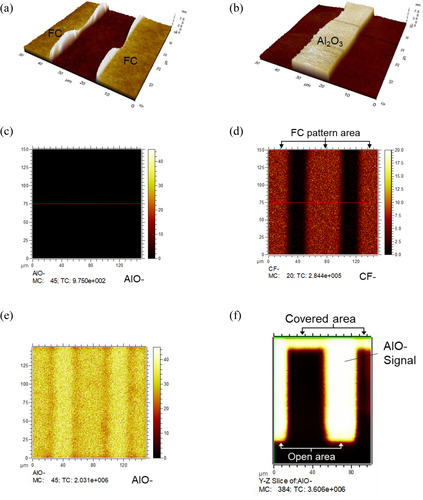
Figure shows optical microscopy images before and after ultrasonic agitation in acetone of Al2O3-deposited PR pattern for lift-off patterning. The Al2O3-deposited PR pattern showed a wrinkled surface (Figure (b)) compared to the surface prior to the ultrasonic agitation (Figure (a)), and the Al2O3-deposited PR pattern could not be removed even after 15 min of ultrasonic agitation. Further, considering that the Al2O3 deposited PR surface is reasonably smooth with fine grains as seen in the AFM surface analysis, it can be inferred that the dense Al2O3 film eventually grew on the PR pattern surface through subsequent exposure to TMA and H2O. Other studies have reported that TMA is physically adsorbed and provides nucleation sites for Al2O3 film growth with a polymer-blocking layer, although TMA does not react chemically [Citation18,Citation19,Citation21].
Figure 7. Optical microscope images before and after ultrasonic agitation using acetone for Al2O3-deposited PR pattern: (a) Al2O3 deposited PR patterns; (b) Al2O3-deposited PR pattern after 15-min ultrasonic agitation.
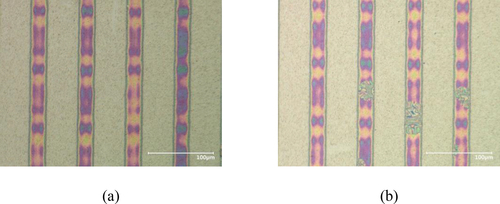
Figure 8. Results of AFM and TOF-SIMS analyses of Al2O3 AS-ALD process using FC/PR inhibition pattern: (a) three-dimensional image and (b) cross-sectional profile of patterned Al2O3 measured by AFM; (c) TOF-SIMS AlO– signal after lift-off process using 0.45 µm thick FC/PR pattern; (d) TOF-SIMS AlO- signal and (e) Si– signal after lift-off process using 1.28 µm thick FC/PR pattern; (f) TOF-SIMS depth intensity of AlO– signal in the background and 1.28 µm thick FC/PR pattern regions.
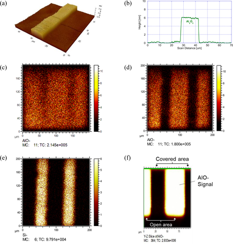
Figure shows the AFM and TOF-SIMS surface analyses results of the lift-off patterning of Al2O3 using the FC/PR pattern. We prepared two FC/PR patterns fabricated using 0.45 and 1.28 μm-thick PR as ALD-inhibition test specimens. The unwanted FC/PR lift-off patterns were removed by ultrasonic agitation using acetone solution for 7 min, regardless of the printed PR thickness. Figures (a) and (b) show cross-sectional profiles and three-dimensional images on patterned Al2O3 measured by AFM. An 18 μm wide and 6 nm thick Al2O3 pattern was obtained on the silicon substrate. In the case of the 0.45 μm thick FC/PR pattern, AlO– was detected everywhere, as shown in the TOF-SIMS mapping image in Figure (c). However, in the case of the 1.28 μm thick FC/PR pattern, AlO– was clearly detected in the shape of Al2O3 patterns (Figure (d)), and the signal of Si– appeared only in the background area (Figure (e)). Also, in the depth profile analysis, AlO– was not detected underneath the FC/PR patterns (Figure (f)). Thus, a 1.28 μm thick FC/PR pattern could entirely block Al2O3 growth and ensure successful AS-ALD. The Al2O3 AS-ALD process using the FC/PR pattern can be inferred as follows: the FC film partially blocks Al2O3 nucleation leading to porous Al2O3 film; and second, 1.28 μm-thick PR pattern blocks Al2O3 cluster diffusion to Si surface. Acetone resolves the PR mask pattern underneath the Al2O3 film through cavities of the porous Al2O3 film, leading to the lift-off of undesired Al2O3 film for the patterning process. In general, to make the acetone penetrate the conformal Al2O3 and attack PR below, manual scratching of the Al2O3 surface is necessary [Citation7,Citation20,Citation22]. However, in our study, the Al2O3 film was successfully patterned by a lift-off process using an inkjet-printed FC/PR blocking layer and ultrasonic agitation without manual scratching.
4. Conclusion
In this study, AS-ALD of Al2O3 was successfully demonstrated using ALD inhibition patterns consisting of a two-layer structure formed by inkjet printing. An FC thin film was coated to inhibit Al2O3 nucleation and growth during the ALD process after thick PR was inkjet-printed to allow easy removal of ALD-inhibition patterns by the lift-off process. The thickness of the inkjet-printed FC pattern was about 3–8 nm owing to a coffee–ring effect. The thickness of the PR line pattern increased from 0.45–1.28 μm for the 30 μm line width by layer–by–layer printing without a coffee–ring effect. To confirm the proposed AS-ALD process, FC, PR, and FC/PR were printed as ALD-inhibition test patterns on Si substrates. Thereafter, a ∼10 nm thick Al2O3 thin film was deposited via an in-house built system with a multiple-slit gas source. The Al2O3 film was successfully patterned by a lift-off process using an FC-covered 1.28 μm-thick PR inhibition layer and ultrasonic agitation. In the TOF-SIMS depth profile analysis, AlO– was not detected underneath the FC/PR patterns. By combining the AFM, surface profilometry, and TOF-SIMS analyses results, inferences can be made regarding the developed AS-ALD mechanism. The FC film partially blocked Al2O3 nucleation leading to porous Al2O3 film, while the thick PR pattern additionally blocked Al2O3 cluster diffusion to the Si surface. The sonicated acetone resolves the PR mask pattern underneath the Al2O3 film through cavities of porous Al2O3, leading to lift off of undesired Al2O3film for the patterning process. In the case of the FC pattern, although Al2O3 was physically patterned by O2 plasma, AlO– was detected in the FC pattern-blocked area by TOF-SIMS depth profile analysis. Also, for the PR pattern, the Al2O3-deposited PR mask could not be removed even after 15 min of ultrasonic agitation. Our study demonstrated an efficient patterning performance of the inkjet printing process to form inhibition patterns for AS-ALD. The developed inkjet printing process successfully patterned multilayer structures with different thicknesses and surface properties by precisely positioning target materials on a substrate using computer control. This process can be used as an effective method for patterning inorganic thin films for low-cost, large-area, flexible electronic components without using a photolithography patterning process.
Disclosure statement
No potential conflict of interest was reported by the author(s).
Additional information
Funding
Notes on contributors

Jun Ho Yu
Jun Ho Yu received his B.S. degree in biotechnology from Chung–Ang University, Anseong, Korea, in 2007 and his M.S. degree in advanced materials engineering from Sungkyunkwan University, Suwon, Korea, in 2016. In 2010, he joined the Micro/Nano Scale Manufacturing R&D Group, Korea Institute of Industrial Technology, where he is currently a researcher. His research interests include inkjet-based printed electronics and laser material processing

Young–In Cho
Young–In Cho received his B.S. degree in material engineering from Han–Yang University, Ansan, Korea, in 2017 and his M.S. degree in material engineering from Han–Yang University, Seoul, Korea, in 2019. In 2017, he joined the Micro/Nano Scale Manufacturing R&D Group, Korea Institute of Industrial technology.

Jae–Wook Lee
Jae–Wook Lee received his B.S. degree in Mechatronics Engineering from Jeju National University, Jeju, Korea, in 2015 and his M.S. degree in Mechatronics Engineering from Jeju National University, Jeju, Korea, in 2018. In 2019, he joined as a Ph.D. candidate in Mechatronics Engineering at Jeju National University. His research interests include atomic layer deposition based on spatial and roll–to–roll methods.

Kyung Hyun Choi
Kyung Hyun Choi received his B. S. and M. S. degrees from Pusan National University, Pusan, Korea, in 1985 and 1990, respectively, and his Ph.D. degree from the University of Ottawa, Canada, in 1995. He is a professor of Mechatronics Engineering at Jeju National University in South Korea. His current research interests involve printed electronics and devices such as OLED, OPV, and Memristor.

Sang–Ho Lee
Sang–Ho Lee received his B. S. degree in Metallurgy and Materials Science Engineering from Hanyang University in 1996 and Ph.D. degree in Electrical Engineering from Seoul University in 2003. He joined Korea Institute of Industrial Technology in 2006 after a two-year post-doctoral fellowship at Soh Lab, UCSB. His current research interests involve micro biodevices, paper chips, printed electronics and application of industrial inkjet technology.
References
- M. Leskelä, and M. Ritala, Thin Solid Films 409 (1), 138–146 (2002).
- M. Fang, and J.C. Ho, ACS Nano 9 (9), 8651–8654 (2015).
- A.J.M. Mackus, A.A. Bol, and W.M.M. Kessels, Nanoscale 6 (19), 10941–10960 (2014).
- W. Lee, N.P. Dasgupta, O. Trejo, J–R Lee, J. Hwang, T. Usui, and F.B. Prinz, Langmuir 26 (9), 6845–6852 (2010).
- A. Haider, P. Deminskyi, T.M. Khan, H. Eren, and N. Biyikli, J Phys Chem C 120 (46), 26393–26401 (2016).
- F.S. Minaye Hashemi, C. Prasittichai, and S.F. Bent, ACS Nano 9 (9), 8710–8717 (2015).
- E. Färm, M. Kemell, M. Ritala, and M. Leskelä, J Phys Chem C 112 (40), 15791–15795 (2008).
- M.H. Park, Y.J. Jang, H.M. Sung–Suh, and M.M. Sung, Langmuir 20 (6), 2257–2260 (2004).
- C.R. Ellinger, and S.F. Nelson, Chem Mater 26 (4), 1514–1522 (2014).
- Z–Y Wang, R–J Zhang, H–L Lu, X. Chen, Y. Sun, Y. Zhang, Y–F Wei, and J–P Xu, Nanoscale Res Lett 10 (46), 1–6 (2015).
- D. Li, L. Ruan, J. Sun, C. Wu, Z. Yan, J. Lin, and Q. Yan, Nanotechnol Rev 9, 876–885 (2020).
- M.D. Groner, J.W. Elam, F.H. Fabreguette, and S.M. George, Thin Solid Films 413 (1–2), 186–197 (2002).
- M.D. Groner, S.M. George, R.S. McLean, and P.F. Carcia, Appl Phys Lett 88, 051907 (2006).
- J. Meyer, A.D. Schneidenbach, T. Winkler, S. Hamwi, T. Weimann, P. Hinze, S. Ammermann, H.H. Johannes, T. Riedl, and A.A.W. Kowalsky, Appl Phys Lett 94, 233305 (2009).
- Z.Y. Nuru, C.J. Arendse, S. Khamlich, and M. Maaza, Vacuum 86 (12), 2129–2135 (2012).
- Y.J. Jo, H.S. Jin, M–W Ha, and T.J. Park, Electronic Materials Lett 15, 179–185 (2019).
- J. Lee, J.H. Kim, and S. Im, Appl Phys Lett 83, 2689 (2003).
- S. Seo, B.C. Yeo, S.S. Han, C.M. Yoon, J.Y. Yang, J. Yoon, C. Yoo, H–J Kim, Y. Lee, S.J. Lee, and J–M Myoung, ACS Appl Mater Interfaces 9, 41607–41617 (2017).
- A. Haider, P. Deminskyi, T.M. Khan, H. Eren, and N. Biyikli, Phys Chem C 120 (46), 26393–26401 (2016).
- E. Färm, M. Kemell, E. Santala, M. Ritala, and M. Leskelä, J Electrochem. Soc 157 (1), K10–K14 (2010).
- C.A. Wilson, R.K. Grubbs, and S.M. George, Chem Mater 17 (23), 5625–5634 (2005).
- M.J. Biercuk, D.J. Monsma, and C.M. Marcus, Appl Phys Lett 83, 2405 (2003).
- D.H. Levy, C.R. Ellinger, and S.F. Nelson, Appl Phys Lett 103 (4), 043505 (2013).
- E.K. Seo, J.W. Lee, H.M. Sung–Suh, and M.M. Sung, Chem. Mater 16 (10), 1878–1883 (2004).
- M. Yan, Y. Koide, J.R. Babcock, P.R. Markworth, J.A. Belot, T.J. Marks, and R.P.H. Chang, Appl Phys Lett 79 (11), 1709–1711 (2001).
- L. Guo, I. Lee, and F. Zaera, ACS Appl Mater Interfaces 8 (30), 19836–19841 (2016).
- L. Guo, and F. Zaera, Nanotechnology 25 (50), 504006 (2014).
- X. Jiang, and S.F. Bent, J Phys Chem C 113 (41), 17613–17625 (2009).
- B. Kim, M.L. Geier, M.C. Hersam, and A. Dodabalapur, ACS Appl Mater Interfaces 7 (50), 27654–27660 (2015).
- H. Meier, U. Löffelmann, D. Mager, P.J. Smith, and J.G. Korvink, Phys Status Solidi A 206 (7), 1626–1630 (2009).
- K. Ali, and K–H Choi, Langmuir 30, 14195–14203 (2014).
- K. Ali, K–H Choi, and N.M. Muhammad, Chemical Vapor Deposition 20, 380–387 (2014).
- Y–I Cho, J.H. Yu, D.G. Yoon, J–G Park, K.H. Choi, and S–H Lee, SID 49 (1), 1478–1481 (2018).
- S. Sim, S–H Lee, K.H. Cho, and J.H. Yu, J Electric Engg Technol 16 (4), 2157–2165 (2021).
- J.H. Yu, K–H Cho, K–T Kang, Y–I Cho, C–S Lee, and S–H Lee, SID 49 (1), 843–846 (2018).