
 ?Mathematical formulae have been encoded as MathML and are displayed in this HTML version using MathJax in order to improve their display. Uncheck the box to turn MathJax off. This feature requires Javascript. Click on a formula to zoom.
Abstract
Here, we report the fabrication of high-performance printable WSe2 transistors via the doping of p-type FeCl3 molecules (hole mobility: ∼1.5 cm2 V−1 s−1; on/off ratio: ∼106). A complementary inverter is demonstrated with p-WSe2 and n-MoS2 transistors, which highlights its potential for application in future two-dimensional material-based printable electronics.
1. Introduction
The past few decades have witnessed the rapid development of inks based on two-dimensional (2D) materials owing to their potential for diverse industrial applications, including energy harvesting and conversion, sensors, photovoltaics, and flexible electronics [Citation1]. Among them, transition metal dichalcogenides (TMDs) are a promising and unique class of materials, and have been used as building blocks in fundamental printable (opto)electronic applications, such as thin-film transistors (TFTs), superconductors, supercapacitors, detectors, and logic circuits [Citation2,Citation3], due to their versatility from insulators, semiconductors, semimetals, to metals [Citation4].
Recent research has particularly focused on 2D complementary metal–oxide semiconductor (CMOS) technology [Citation5] since it forms the backbone of integrated circuits. However, most solution-processed CMOS circuits based on 2D TMD inks were fabricated by integrating n-type MoS2 with p-type carbon nanotubes (CNTs) or organic semiconductors [Citation6-8], but rarely were they fabricated with p-type 2D TMD semiconductors [Citation5]. This was mainly due to the inferior electrical performance of solution-processed p-type TMD transistors compared to that of n-type ones, resulting in a considerable mismatch in the device performance when applying CMOS technology. For instance, a solution-processed p-type transistor fabricated with undoped 2D WS2 semiconductors exhibited a mobility of 0.22 cm2 V−1 s−1,and an on/off ratio of approximately 102 [Citation9]. In contrast, solution-processed MoS2 TFTs were reported to exhibit a mobility of approximately 10 cm2 V−1 s−1, with a high on/off ratio of approximately 106 [Citation3,Citation8,Citation10], while In2Se3 TFTs exhibited mobility of 0.4 cm2 V−1 s−1 and an on/off ratio of approximately 103 [Citation11]. The low hole mobility of solution-processed p-type 2D TMD TFTs consisting of aligned nanoflakes can primarily be attributed to the high contact resistance and inefficient carrier transport in the channel [Citation12,Citation13].
Fermi-level pinning at metal contacts to create a large hole Schottky barrier height (SBH) can contribute to high contact resistance. Although metals of different work functions have been used, the SBH was still over 1 eV for hole injection [Citation14]. Further, obtaining an ultra-clean surface and high-quality 2D semiconductors by liquid-phase exfoliation compared to mechanical exfoliation can be challenging. Hence, the existence of surface impurities and intrinsic defects originating from the 2D semiconductor could induce Fermi-level pinning [Citation15]. On the other hand, the resistance among nanoflakes could also contribute to a high channel resistance, hindering charge transport [Citation13]. The interfacial resistance in 2D semiconductor films could reach 100 GΩ, significantly higher than the interfacial resistance (1-5 MΩ) [Citation16]. To overcome the aforementioned limitations, molecular doping has been considered an effective approach for improving the electrical properties of solution-processed TFTs, and this was proven for mechanically exfoliated single-flake transistors. For instance, Kim et.al demonstrated the depinning of the Fermi level via molecular doping onto a MoTe2 channel to significantly lower the SBH and reduce the contact resistance [Citation17]. Lee et.al revealed that the carrier density and conductivity of WSe2 can be more effectively modulated by using an appropriate molecular dopant, and that the amount of charge transfer between WSe2 and the dopants is determined by both, the doping density and the contribution of each dopant ion toward Coulomb scattering [Citation18]. In addition, molecular doping has been shown to be advantageous in terms of being a relatively non-destructive process and being applicable with a diverse range of potential dopants [Citation19].
Hence, in this study, we selected iron (III) trichloride (FeCl3), an oxidative dopant that has been widely used as a p dopant in organic semiconductors [Citation20,Citation21], as a representative dopant to achieve the desired device performance for solution-processed p-type WSe2 TFTs. The doped WSe2 TFTs exhibited typical p-type behavior compared to the ambipolar behavior for pristine devices. We systematically investigated the influence of the FeCl3 concentration on the solution-processed WSe2 TFTs to modulate the contact resistance, carrier concentration, and trap density. We also developed a simple photolithography process with drop-casting to pattern the semiconducting films, which enabled us to integrate n-type and p-type TMD TFTs for fabricating printable CMOS inverters.
2. Results and discussion
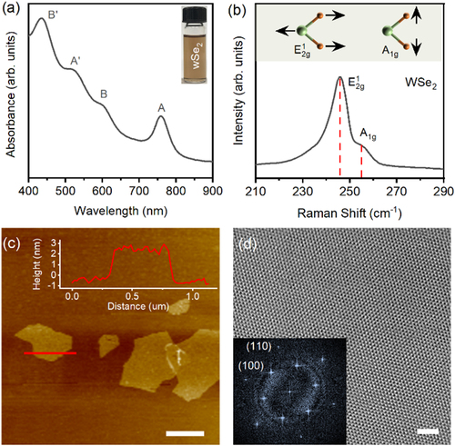
WSe2 nanoflakes were prepared as p-type transistors through an electrochemical intercalation approach, according to the literature [3]. Briefly, tetraethylammonium bromide (THAB) dissolved in acetonitrile was used as the electrolyte. A copper plate with an attached WSe2 crystal was used as the cathode, and a graphite rod was used as the opposite anode. Subsequently, a voltage of 15 V was applied for 1 h to intercalate the WSe2 crystal. The intercalated WSe2 crystal was then sonicated in dimethylformamide (DMF)/polyvinylpyrrolidone (PVP) solution for 30 min. Finally, the obtained WSe2 nanoflakes were washed and dispersed in isopropanol (IPA). The ultraviolet (UV)-visible spectrum in Figure (a) shows two feature peaks at A (761 nm) and B (590 nm), which are mainly attributed to the splitting of the valence band due to spin–orbit coupling [Citation22]. The origination of the other two peaks at A′ (518 nm) and B′ (436 nm) is believed to be the perturbation to the d electron band by the Se p orbitals, which causes the splitting of the ground and excited states of A and B transitions, separately [Citation23]. The Raman spectrum in Figure (b) shows characteristic E2g1 (246 cm−1) and A1g (254 cm−1) peaks, corresponding to transition metal and chalcogen atoms’ in-place displacement and out-of-plane vibration of chalcogen atoms, respectively [Citation24]. The WSe2 nanoflakes also exhibit a PL peak at 1.64 eV (Figure S2). The atomic force microscopy (AFM) image in Figure (c) shows that the exfoliated WSe2 nanoflakes have a lateral dimension of 1–2 µm and a thickness of ∼3 nm. The high-resolution transmission electron microscopy (HRTEM) image reveals that the exfoliated WSe2 nanoflakes have a high crystallinity (Figure (d)). The electron hexagonal diffraction pattern shows that the interlayer distance of the (100) plane is 0.28 nm, in agreement with the reported distance in WSe2 [Citation25]. We also prepared MoS2 inks by the same electrochemical intercalation approach and similarly characterized as the prepared MoS2 nanoflakes. The results are shown in Figure S1-3. The findings confirm the successful preparation of semiconducting 2H-phase WSe2 and MoS2 nanoflakes.
Figure 1. (a) UV-visible spectrum of the as-prepared WSe2 solution. The inset shows the photograph of each dispersion in isopropanol. (b) Raman spectra of WSe2. The inset shows the atomic displacement of the E2g1 and A1g Raman-active modes. (c) AFM image of the exfoliated WSe2 nanoflakes and the corresponding height profile (scale bar: 500 nm). (d) High-resolution TEM image of the exfoliated WSe2 nanoflakes. The inset shows the selected-area electron diffraction image (scale bar: 2 nm).
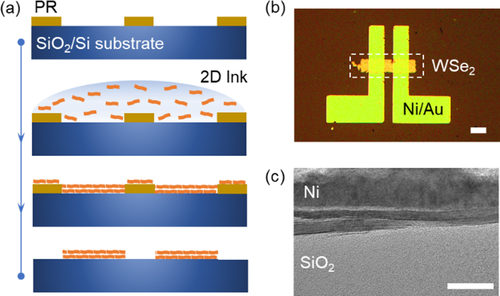
Different methods have been explored to fabricate patterned semiconductor thin films, such as spin coating [Citation3], inkjet or spray printing [Citation8], and layer-by-layer (LbL) assembly [Citation10]. However, spin coating typically requires an additional reactive ion etching (RIE) process to pattern the channel, while for inkjet printing, the surface tension and viscosity of the ink should be optimized well. To simplify the fabrication process, in this study, we patterned the solution-processed TMD thin films by photolithography and drop-casting (Figure (a)). Firstly, a photoresist (PR) was patterned via photolithography to define the desired area for the semiconductor film. In this study, the SU-8 (Kayaku Advanced Materials, Inc.) PR was selected because it can survive from the immersion in IPA after crosslinking with UV exposure. Subsequently, 2D inks were drop-casted on the patterned PR and dried slowly. The substrate was covered with a Petri dish. In this way, the IPA vapor could retard the solvent evaporation rate. The liquid WSe2 solution on the substrate will become thinner slowly, and the concentration of the solution will increase gradually. Thus, the WSe2 nanoflakes tend to vertically stack together to form a high-quality and fine alignment of WSe2 thin film. We then stripped off the PR, leaving only the patterned semiconductor thin film on the substrate. To complete the transistor fabrication, the substrate with the semiconductor thin film was annealed on a hotplate in a nitrogen-filled glovebox at 200 °C for one hour to evaporate the IPA solvent. Finally, the electrodes were thermally evaporated and patterned via photolithography. Figure (b) shows the WSe2 TFT with a patterned and compact semiconductor thin film. The edge between the semiconductor thin film and substrate is distinguishable. The cross-sectional TEM image (Figure (c)) shows that the film has multiple overlapping flakes with a clearly distinguishable interface between the flakes. The layered structures are parallel to the surface and have a thickness of ∼10 nm. In the transistor fabrication process, most processes were conducted in ambient conditions, except for the annealing step in the glove box and electrode deposition in a high-vacuum chamber. Thus, our method is low-cost and easy and could be applicable for large-scale assembly and the fabrication of flexible or wearable complex circuits with 2D functional materials.
Figure 2. (a) Schematic of transistor fabrication by drop-casting with the 2D ink. (b) Optical micrograph of the as-fabricated WSe2 transistor (scale bar: 100 µm). (c) Cross-sectional TEM image of the WSe2 thin film on the Si/SiO2 substrate (scale bar: 20 nm).
Furthermore, we investigated the electrical properties of the as-prepared WSe2 TFTs. The IDS–VGS transfer curve (Figure (a)) reveals an ambipolar behavior for the pristine WSe2 TFT, with hole and electron conduction occurring below −15 V and above 40 V, respectively, implying a Fermi-level pinning effect that can be modulated by molecular doping [Citation17]. Consequently, the pristine WSe2 TFT exhibits a low on/off ratio of ∼5 × 10³. The field-effect channel mobility (µFE) was estimated using the following equation:
where L is the channel length, W is the channel width, Ci is the gate dielectric capacitance per unit area, and VDS is the applied source–drain voltage. The pristine WSe2 TFT had a low hole µFE of 1.5 × 10⁻³ cm2 V−1 s−1.
Figure 3. (a) IDS–VGS transfer curves at VDS = −1 V for the pristine and FeCl3-doped WSe2 (60 µg/mL) TFTs on a SiO2/Si substrate with a 100 nm-thick SiO2 layer. VDS is −1 V. The width and length of the channel are 725 and 50 µm, respectively. (b) Output curve of the corresponding FeCl3-doped WSe2 TFT. (c) UPS spectra showing the secondary electron cut-off and (d) valence band of pristine and FeCl3-doped WSe2 thin films (60 µg/mL). (e) Schematic energy diagram of the Ni/Au and WSe2 contacts before and after doping. (f) Schematic energy diagram at the interface between the nanoflakes in the channel with a bias voltage applied after doping.
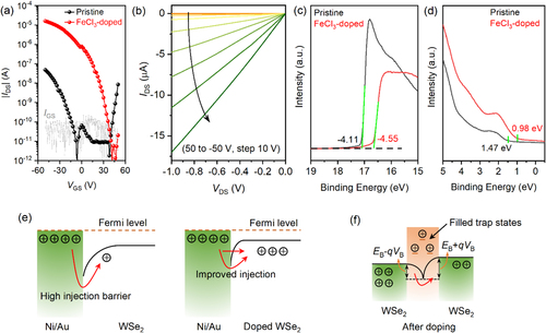
FeCl3 was applied as a dopant to modulate the electronic properties and control the carrier concentration. In this procedure, FeCl3 powders were dissolved in 1,2-dichlorobenzene solvent to obtain solutions of different concentrations. The pristine device was then immersed in the FeCl3 solutions and annealed at 80°C for 30 min in ambient conditions. After doping with FeCl3, the IDS–VGS transfer curve showed clear p-type characteristics with an increased on-current at VGS = −50 V and a positive shift in the threshold voltage (Vth), representing a p-doing effect. The resulting WSe2 TFT showed a significantly improved µFE up to 1.0 cm2 V−1 s−1, which is approximately three orders of magnitude higher than the pristine WSe2 TFT. Note that our FeCl3-treated WSe2 TFT maintained a low off-current below 1 × 10⁻¹¹ A and showed a high on/off ratio of ∼3.0 × 10⁶, unlike reported results where some doping treatments had negatively affected the on/off ratio [Citation26,Citation27]. The output curve after FeCl3 doping also indicated that the WSe2 TFT had a relatively low contact resistance (Figure (b)). Thus, our doping method achieves better device mobility and on/off ratio than the pristine WSe2 TFT and other reported solution-processed p-type 2D TMD TFTs [Citation9,Citation13]. Our obtained values are comparable to those of solution-processed n-type 2D TMD transistors [Citation3,Citation8,Citation10]. A detailed comparison is provided in Table S1.
The doped hole carrier density can be regulated according to the FeCl3 concentration, as evidenced by the IDS–VGS transfer curve (Figure S4a). With increasing FeCl3 concentration, there is a gradual positive shift in Vth from −35 V for the pristine device to −10 V after treatment with a 120 µg/mL FeCl3 solution. Increasing the FeCl3 solution concentration to 120 µg/mL results in a hole µFE of ∼1.5 cm2 V−1 s−1 and a high on/off ratio of 1.4 × 10⁶ (Figure S4b). However, using a higher doping concentration can introduce excess charges in the WSe2 thin film, ultimately increasing the off-current. Consequently, a larger positive bias is needed to f deplete the excess charges and turn off the device fully. The hole density (n_hole) of the FeCl3-doped WSe2 TFT was calculated using the equation n_hole = (IDSL)/(qWVDSµ), where q is the electron charge [Citation26,Citation28]. The calculated n_hole as a function of the FeCl3 solution concentration is plotted in Figure S5. The n_hole at VGS = 0 V increases from 8.4 × 10¹¹ to 5.1 × 1012 cm−2 with an increase in the FeCl3 solution concentration from 1.2–120 µg/mL. The hole density of the undoped WSe2 film is estimated to be approximately 5 × 1011 cm−2. The amount of generated carrier hole density by doping is comparable to previously reported data (3.6 × 1012 cm−2 for F4-TCNQ-doped WSe2 and 4.5 × 1012 cm−2 for Mo(tfd-COCF3)3-doped WSe2) [Citation18].
Ultraviolet photoemission spectroscopy (UPS) is a direct measurement method to demonstrate the doping effect and work function change [Citation29]. The secondary electron cut-off spectrum (Figure (c)) shows a downward shift in the Fermi level from −4.11 eV to −4.55 eV after the FeCl3 treatment of the WSe2 thin film. The distance between the valence-band maximum (EVBM) to the Fermi level (EF) also shifts from 1.47 eV to 0.98 eV (Figure (d)). The downshift of EF to EVBM indicates the occurrence of considerable electron transfer from the WSe2 to FeCl3 molecules, i.e. the p-type doping effect in the WSe2 film, which may be attributed to the low electron affinity (EA) of the oxidizing agent, FeCl3 (EA = −4.65 eV) [Citation21,Citation30].
The downshift in EF for the FeCl3-doped WSe2 TFT would also lower the SBH and narrow the depletion region, facilitating easier hole injection (Figure (e)) [Citation31]. In contrast, for the pristine WSe2 TFT, carrier injection is dominated by thermionic emission because of the large SBH and thick depletion layer due to the Fermi-level pinning effect. The contact resistance (Rc) was extracted by the Y-function method [Citation32]. Rc considerably decreased to 3.1 × 10³ kΩ µm after FeCl3 doping, which is approximately three orders of magnitude lower than that of the pristine WSe2 TFT (2.3 × 10⁶ kΩ µm). We propose that the high on/off ratio observed after FeCl3 p-doping can be attributed to the reduction in the SBH for hole injection with moderate doping concentration, resulting in a decrease in contact resistance. First, the effectively reduced hole SBH through moderate p-doping facilitates hole injection, increasing the effective SBH for electrons. Second, the moderate p-doping can enhance the conductivity of the channel and reduce the electron concentration in the 2D semiconductor layer. Meanwhile, moderate doping allows the applied gate voltage to completely deplete the introduced free charges in the device. These effects are advantageous for achieving a high on-state current and a low off-current.
On the other hand, the subthreshold swing (SS) decreased from 4.0 V/dec for the pristine WSe2 TFT to 2.6 V/dec after FeCl3 treatment. Accordingly, the total trap density (Ntrap) values were estimated to be 1.52 × 1013 cm−2 eV−1 and 9.8 × 1012 cm−2 eV−1 for the pristine and FeCl3-doped WSe2 TFTs, respectively [Citation33]. Trap states are typically generated at the gate insulator/semiconductor interface and interflake interfaces because of the bubbles or wrinkles. They can induce scattering of the charge carriers, thereby hindering carrier transport [Citation34]. Our results indicate that the generated free carriers by p-doping can fill the trap states and effectively screen the trapped charges (Figure (f)), leading to increased carrier mobility. Based on the theoretical model of charge transport on grain boundaries [Citation35,Citation36], the effective height of the potential barrier on the forward bias side is EB-qVB, which plays a significant role in charge transport, and that on the reverse bias is EB + qVB, where EB is the height of potential barrier at grain boundaries, and VB is the voltage drop across grain boundaries. The doping effect can modulate the effective height of the potential barrier by influencing the total carrier density, the resistance from the grain boundaries and the crystallite, and so on [Citation35]. To obtain a precise and quantitative analysis of the dependence of the height of the barrier on the doping, a proper theoretical model and additional experiments are required for 2D thin film systems.
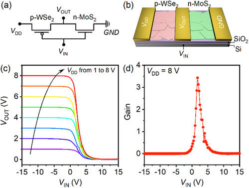
Based on the aforementioned lift-off-based patterning method, we fabricated a CMOS inverter composed of solution-processed p-WSe2 and n-MoS2 TFTs (Figure (a,b)). The WSe2 thin film was first deposited on a 100 nm-thick SiO2/Si substrate, following which the MoS2 thin film was deposited. Our n-MoS2 TFTs exhibited a mobility of ∼5 cm2 V−1 s−1 after treatment with bis(trifluoromethane)sulfonimide (TFSI) (Figure S6), similar to the previous report [Citation3,Citation37]. The drain currents of the p-WSe2 and n-MoS2 TFTs were adjusted to the same level by controlling the channel width and doping concentration. The CMOS inverters exhibited an ideal steep switching behavior in the voltage transfer characteristic curve (Figure (c)). A voltage gain of 3.5 was achieved under a driving voltage (VDD) of 8 V (Figure (d)). The gain was comparable to previously reported study on a printed CNT/MoS2 CMOS inverter (Table S2) [Citation7,Citation8]. We expect to attain higher gains through further optimization of the subthreshold slope by increasing the gate insulator capacitance per unit area [Citation38].
Figure 4. Solution-processed complementary metal-oxide-semiconductor (CMOS) inverter. (a) Circuit diagram of the CMOS inverter. (b) Schematic of a CMOS inverter with p-WSe2 and n-MoS2 channels. (c) Voltage transfer characteristics of the CMOS inverter as a function of the input voltage with different VDD values from 1 to 8 V. The FeCl3-doping concentration for p-WSe2 is 60 µg/mL. (d) Corresponding gains of the inverter from c at VDD = 8 V.
3. Conclusion
Our work demonstrates a general molecular doping approach to fabricate high-performance solution-processed p-channel transistors using WSe2 semiconductors. We also present a simple photolithography process involving drop-casting to obtain a patterned semiconducting film. Thus, we successfully demonstrate the fabrication of a CMOS inverter integrated with p-type WSe2 and n-type MoS2 semiconductors. Most importantly, this study provides a series of robust routes to use 2D material inks and integrate multiple semiconductors to realize printable electronic devices. Therefore, our work paved the way for future ultrathin, flexible, and wearable electronic and optoelectronic applications.
Disclosure statement
No potential conflict of interest was reported by the author(s).
Additional information
Funding
Notes on contributors

Taoyu Zou
Taoyu Zou received his M.S. degree from the Department of Physics and Astronomy of Yunnan University, China, in 2016. He is currently a Ph.D. candidate at the Department of Chemical Engineering of the Pohang University of Science and Technology (POSTECH) under the supervision of Prof. Yong-Young Noh. His current research interests include solution-processed 2D materials for thin-film transistors and circuits.

Haksoon Jung
Haksoon Jung is currently a Ph.D. student in the Department of Chemical Engineering at Pohang University of Science and Technology (POSTECH) under the supervision of Prof. Yong-Young Noh. He received his B.S. degree from the Department of Energy and Materials Engineering of Dongguk University, Korea, in 2019. His research interests include emerging semiconductor materials and devices.

Ao Liu
Ao Liu is a postdoc at the Department of Chemical Engineering of Pohang University of Science and Technology (POSTECH). He received his Ph.D. degree from the Department of Chemical Engineering at Pohang University of Science and Technology (POSTECH) in 2022. His research interests include the development of solution-processed metal oxide/organic materials and their applications in transistors and circuits.

Soonhyo Kim
Soonhyo Kim received his B.S. degree in Chemical Engineering from the Pohang University of Science and Technology (POSTECH) in 2020. He is currently a Ph.D. candidate in the Department of Chemical Engineering at POSTECH under the supervision of Prof. Yong-Young Noh. His research interests include the development of semiconductors for transistors based on computational and experimental methods.

Youjin Reo
Youjin Reo received her B.S. degree in Chemical Engineering from the Pohang University of Science and Technology (POSTECH) in 2020. She is currently a Ph.D. candidate in the Department of Chemical Engineering at POSTECH under the supervision of Prof. Yong-Young Noh. Her research interests include the development of perovskite-based semiconductors through solution-process and thermal deposition, as well as their applications in transistors and circuits.

Taesu Choi
Taesu Choi received his B.S. degree in Chemical Engineering from the Pohang University of Science and Technology (POSTECH) in 2020. He is currently a Ph.D. candidate in the Department of Chemical Engineering at POSTECH under the supervision of Prof. Yong-Young Noh. His research interests include oxide semiconductors by thermal deposition.

Yong-Young Noh
Yong-Young Noh is the Chair Professor of the Department of Chemical Engineering of Pohang University of Science and Technology (POSTECH). He received his Ph.D. degree in 2005 from GIST and then worked at the Cavendish Laboratory in Cambridge, UK, as a postdoctoral associate. Afterward, he worked at ETRI as a senior researcher, as assistant professor at Hanbat National University, and as associate professor at Dongguk University. His research interest is in the field of developing printable semiconductors including 2D materials, organic, carbon nanotubes, perovskite, metal halide and metal oxide for field-effect transistors, photodetectors, and light-emitting diodes.
References
- S. Pinilla, J. Coelho, K. Li, J. Liu, and V. Nicolosi, Nat. Rev. Mater. 7, 717 (2022); T. Taniguchi, L. Nurdiwijayanto, R. Ma, and T. Sasaki, Appl. Phys. Rev. 9, 021313 (2022); G. Hu, J. Kang, L.W.T. Ng, X. Zhu, R.C.T. Howe, C.G. Jones, M.C. Hersam, and T. Hasan, Chem. Soc. Rev. 47, 3265 (2018); S. Abdolhosseinzadeh, X. Jiang, H. Zhang, J. Qiu, and C. Zhang, Two-dimensional material inks. Today 48, 214 (2021); S. Bellani, A. Bartolotta, A. Agresti, G. Calogero, G. Grancini, A. Di Carlo, E. Kymakis, and F. Bonaccorso, Chem. Soc. Rev. 50, 717 (2021).
- Y. Ma, X. Shao, J. Li, B. Dong, Z. Hu, Q. Zhou, H. Xu, X. Zhao, H. Fang, X. Li, Z. Li, J. Wu, M. Zhao, S.J. Pennycook, C.H. Sow, C. Lee, Y.L. Zhong, J. Lu, M. Ding, K. Wang, Y. Li, and J. Lu, ACS Appl. Mater. Interfaces 13, 8518 (2021); J. Li, P. Song, J. Zhao, K. Vaklinova, X. Zhao, Z. Li, Z. Qiu, Z. Wang, L. Lin, M. Zhao, T.S. Herng, Y. Zuo, W. Jonhson, W. Yu, X. Hai, P. Lyu, H. Xu, H. Yang, C. Chen, S.J. Pennycook, J. Ding, J. Teng, A.H. Castro Neto, K.S. Novoselov, and J. Lu, Nat. Mater. 20, 181 (2021); Z. Yan, D. Xu, Z. Lin, P. Wang, B. Cao, H. Ren, F. Song, C. Wan, L. Wang, J. Zhou, X. Zhao, J. Chen, Y. Huang, and X. Duan, Science 375, 852 (2022); B. Li, X. Liang, G. Li, F. Shao, T. Xia, S. Xu, N. Hu, Y. Su, Z. Yang, and Y. Zhang, ACS Appl. Mater. Interfaces 12, 39444 (2020); T. Zou, H.-J. Kim, S. Kim, A. Liu, M.-Y. Choi, H. Jung, H. Zhu, I. You, Y. Reo, W.-J. Lee, Y.-S. Kim, C.-J. Kim, and Y.-Y. Noh, Adv. Mater. 35, 2208934 (2023).
- Z. Lin, Y. Liu, U. Halim, M. Ding, Y. Liu, Y. Wang, C. Jia, P. Chen, X. Duan, C. Wang, F. Song, M. Li, C. Wan, Y. Huang, and X. Duan, Nature 562, 254 (2018).
- M. Chhowalla, H.S. Shin, G. Eda, L.J. Li, K.P. Loh, and H. Zhang, Nat. Chem. 5, 263 (2013).
- L. Kong, Y. Chen, and Y. Liu, Nano Res. 14, 1768 (2021).
- T. Carey, A. Arbab, L. Anzi, H. Bristow, F. Hui, S. Bohm, G. Wyatt-Moon, A. Flewitt, A. Wadsworth, N. Gasparini, J.M. Kim, M. Lanza, I. McCulloch, R. Sordan, and F. Torrisi, Adv. Electron. Mater. 7, 2100112 (2021).
- I. Brunetti, L. Pimpolari, S. Conti, R. Worsley, S. Majee, D.K. Polyushkin, M. Paur, E. Dimaggio, G. Pennelli, G. Iannaccone, M. Macucci, F. Pieri, T. Mueller, C. Casiraghi, and G. Fiori, npj 2D Mater. Appl. 5, 85 (2021).
- J. Kim, D. Rhee, O. Song, M. Kim, Y.H. Kwon, D.U. Lim, I.S. Kim, V. Mazánek, L. Valdman, Z. Sofer, J.H. Cho, and J. Kang, Adv. Mater. 34, 2106110 (2022).
- A.G. Kelly, T. Hallam, C. Backes, A. Harvey, A.S. Esmaeily, I. Godwin, J. Coelho, V. Nicolosi, J. Lauth, A. Kulkarni, S. Kinge, L.D. Siebbeles, G.S. Duesberg, and J.N. Coleman, Science 356, 69 (2017).
- X. Gao, J. Yin, G. Bian, H.-Y. Liu, C.-P. Wang, X.-X. Pang, and J. Zhu, Nano Res. 14, 2255 (2021).
- X. Gao, H.-Y. Liu, J. Zhang, J. Zhu, J. Chang, and Y. Hao, Micromachines 13, 956 (2022).
- Q. He, Y. Liu, C. Tan, W. Zhai, G.H. Nam, and H. Zhang, ACS Nano 13, 12294 (2019).
- A.C. Kelly, D. O'Suilleabhain, C. Gabbett, and J.N. Coleman, Nat. Rev. Mater. 7, 217 (2022).
- G. Kwon, Y.-H. Choi, H. Lee, H.-S. Kim, J. Jeong, K. Jeong, M. Baik, H. Kwon, J. Ahn, E. Lee, and M.-H. Cho, Nat. Electron. 5, 241 (2022).
- Y. Wang and M. Chhowalla, Nat. Rev. Phys. 4, 101 (2022); S. McDonnell, R. Addou, C. Buie, R.M. Wallace, and C.L. Hinkle, ACS Nano 8, 2880 (2014); D. Rhodes, S.H. Chae, R. Ribeiro-Palau, and J. Hone, Nat. Mater. 18, 504 (2019).
- D.C. Moore, A. Jawaid, R. Busch, M. Brothers, P. Miesle, A. Miesle, R. Rao, J. Lee, L.K. Beagle, M. Motala, S.G. Wallace, J.R. Downing, A. Roy, C. Muratore, M.C. Hersam, R. Vaia, S. Kim, and N.R. Glavin, Adv. Funct. Mater. 32, 2106830 (2022).
- C. Kim, I. Moon, D. Lee, M.S. Choi, F. Ahmed, S. Nam, Y. Cho, H.J. Shin, S. Park, and W.J. Yoo, ACS Nano 11, 1588 (2017).
- J.K. Kim, K. Cho, J. Jang, K.Y. Baek, J. Kim, J. Seo, M. Song, J. Shin, J. Kim, S.S.P. Parkin, J.H. Lee, K. Kang, and T. Lee, Adv. Mater. 33, 2101598 (2021).
- S. Bertolazzi, M. Gobbi, Y. Zhao, C. Backes, and P. Samori, Chem. Soc. Rev. 47, 6845 (2018).
- T. Minari, P. Darmawan, C. Liu, Y. Li, Y. Xu, and K. Tsukagoshi, Appl. Phys. Lett. 100, 093303 (2012); T. Sakanoue and H. Sirringhaus, Nat. Mater. 9, 736 (2010); Z. Liang, M.J. Boland, K. Butrouna, D.R. Strachan, and K.R. Graham, J. Mater. Chem. A 5, 093303 (2017).
- Z. Liang, Y. Zhang, M. Souri, X. Luo, A.M. Boehm, R. Li, Y. Zhang, T. Wang, D.-Y. Kim, J. Mei, S.R. Marder, and K.R. Graham, J. Mater. Chem. A 6, 16495 (2018).
- A. Eftekhari, J. Mater. Chem. A 5, 18299 (2017).
- W. Zhao, Z. Ghorannevis, L. Chu, M. Toh, C. Kloc, P.-H. Tan, and G. Eda, ACS Nano 7, 791 (2013); A.R. Beal, J.C. Knights, and W.Y. Liang, J. Phys. C: Solid State Phys. 5, 3540 (1972); R.A. Bromley, R.B. Murray, and A.D. Yoffe, ibid. 5, 759 (1972).
- W. Zhao, Z. Ghorannevis, K.K. Amara, J.R. Pang, M. Toh, X. Zhang, C. Kloc, P.H. Tan, and G. Eda, Nanoscale 5, 9677 (2013).
- S. Fan, S.J. Yun, W.J. Yu, and Y.H. Lee, Adv. Sci. 7, 1902751 (2020).
- D. Kiriya, M. Tosun, P. Zhao, J.S. Kang, and A. Javey, J. Am. Chem. Soc. 136, 7853 (2014).
- P. Zhao, D. Kiriya, A. Azcatl, C. Zhang, M. Tosun, Y.-S. Liu, M. Hettick, J.S. Kang, S. McDonnell, S. Kc, J. Guo, K. Cho, R.M. Wallace, and A. Javey, ACS Nano 8, 10808 (2014); M. Yoon and J. Lee, J. Mater. Chem. C 9, 9592 (2021).
- D. Lee, J.J. Lee, Y.S. Kim, Y.H. Kim, J.C. Kim, W. Huh, J. Lee, S. Park, H.Y. Jeong, Y.D. Kim, and C.-H. Lee, Nat. Electron. 4, 664 (2021).
- R. Guo, Q. Li, Y. Zheng, B. Lei, H. Sun, Z. Hu, J. Zhang, L. Wang, E. Longhi, S. Barlow, S.R. Marder, J. Wang, and W. Chen, Mater. Today 30, 26 (2019).
- Y. Xu, H. Sun, A. Liu, H.-H. Zhu, W. Li, Y.-F. Lin, and Y.-Y. Noh, Adv. Mater. 30, 1801830 (2018).
- H.M. Khalil, M.F. Khan, J. Eom, and H. Noh, ACS Appl. Mater. Interfaces 7, 23589 (2015); Y. Zheng, J. Gao, C. Han, and W. Chen, Cell Rep. Phys. Sci. 2, 100298 (2021); D.S. Schulman, A.J. Arnold, and S. Das, Chem. Soc. Rev. 47, 3037 (2018).
- C. Liu, Y. Xu, and Y.-Y. Noh, Mater. Today 18, 79 (2015).
- Z. Zhang, M. Su, G. Li, J. Wang, X. Zhang, J.C. Ho, C. Wang, D. Wan, X. Liu, and L. Liao, IEEE Electron Device Letters 41, 1036 (2020).
- Q.A. Vu, S. Fan, S.H. Lee, M.-K. Joo, W.J. Yu, and Y.H. Lee, 2D Mater. 5, 031001 (2018); S.J. Haigh, A. Gholinia, R. Jalil, S. Romani, L. Britnell, D.C. Elias, K.S. Novoselov, L.A. Ponomarenko, A.K. Geim, and R. Gorbachev, Nat. Mater. 11, 764 (2012); F. Pizzocchero, L. Gammelgaard, B.S. Jessen, J.M. Caridad, L. Wang, J. Hone, P. Bøggild, and T.J. Booth, Nat. Commun. 7, 11894 (2016).
- Y. Huang, X. Gong, Y. Meng, Z. Wang, X. Chen, J. Li, D. Ji, Z. Wei, L. Li, and W. Hu, Nature Communications 12, 21 (2021).
- G. Baccarani, B. Riccò, and G. Spadini, J. Appl. Phys. 49, 5565 (1978); J.Y.W. Seto, ibid. 46, 5565 (1975).
- M. Amani, D.H. Lien, D. Kiriya, J. Xiao, A. Azcatl, J. Noh, S.R. Madhvapathy, R. Addou, S. Kc, M. Dubey, K. Cho, R.M. Wallace, S.C. Lee, J.H. He, J.W. Ager, 3rd, X. Zhang, E. Yablonovitch, and A. Javey, Science 350, 1065 (2015).
- Z. Luo, B. Peng, J. Zeng, Z. Yu, Y. Zhao, J. Xie, R. Lan, Z. Ma, L. Pan, K. Cao, Y. Lu, D. He, H. Ning, W. Meng, Y. Yang, X. Chen, W. Li, J. Wang, D. Pan, X. Tu, W. Huo, X. Huang, D. Shi, L. Li, M. Liu, Y. Shi, X. Feng, P.K.L. Chan, and X. Wang, Nat. Commun. 12, 1928 (2021); C. Jiang, H.W. Choi, X. Cheng, H. Ma, D. Hasko, and A. Nathan, Science 363, 719 (2019).