
 ?Mathematical formulae have been encoded as MathML and are displayed in this HTML version using MathJax in order to improve their display. Uncheck the box to turn MathJax off. This feature requires Javascript. Click on a formula to zoom.
Abstract
This paper proposes a novel pixel circuit and driving scheme that adopts low-temperature polycrystalline silicon and oxide thin-film transistors (LTPO TFTs) for mobile devices using active-matrix organic light-emitting diode (AMOLED) displays. The proposed pixel circuit and driving scheme provide uniform luminance and render flicker invisible at variable refresh rates (VRRs) from 1 to 120 Hz. Using the proposed pixel circuit with extended compensation time (tCOMP) improves the luminance uniformity at a high-frame rate. The proposed driving scheme applies a voltage to the driving TFTs (D-TFTs) higher than the programmed data voltage during the skip frame. This reduces the flicker caused by the hysteresis of D-TFTs during low-frame rate driving. A 6.0-inch quad high-definition (QHD) LTPO-based AMOLED display was fabricated using the new pixel circuit and driving scheme. Experimental results of the proposed pixel circuit show that the standard deviation of luminance was reduced from 0.056 to 0.008 by extending tCOMP from 2 to 8 µs. The flicker level was −51 dB, so there was no visual artifact during 1 Hz driving. A flicker-free LTPO-based AMOLED display with low power consumption is possible; driving can proceed in 1–120 Hz range.
1. Introduction
In recent years, display backplane technology has been developed from hydrogenated amorphous silicon (a-Si:H) thin-film transistors (TFTs) to low-temperature polycrystalline silicon (LTPS) TFTs and then to low-temperature polycrystalline silicon and oxide (LTPO) TFTs [Citation1–4]. Specifically, LTPO TFTs constitute the next-generation backplane technology for smartphones and smartwatches using active-matrix organic light-emitting diode (AMOLED) display because such devices must be driven at high- and low-frame rates (i.e. variable refresh rate [VRR]) in a power-efficient manner [Citation17,Citation27]. A VRR driving is required for the following reasons: Fast-motion image scenarios, such as gaming and display scrolling, demand a high-frame rate of up to 120 Hz, whereas a low-frame rate down to 1 Hz is appropriate in low-power standby scenarios, such as the always-on display (AOD) and text mode. However, a VRR may exhibit poor compensation performance at high-frame rates and high flicker levels at low-frame rates [Citation5].
Deterioration of compensation performance in high-frame rates causes luminance non-uniformity. As the required frame rate increases, the scan time (tSCAN) of one row is shortened; the compensation time (tCOMP) is now too short to reduce the threshold voltage (VTH) variation, and compensation performance deteriorates. The pixel circuits in one row can acquire voltages from only the data lines within the tSCAN. Therefore, a short tSCAN may cause the tCOMP to be too short for the voltage programming method, resulting in the compensation error for luminance non-uniformity [Citation2,Citation6,Citation15]. If the stored voltage is not exactly equal to the real VTH of the driving TFT (D-TFT), the voltage-programmed pixel circuits are prone to imperfect compensation due to the limited tSCAN available. In other words, to ensure the image quality of a high-frame-rate display, tCOMP should not be limited by tSCAN. However, in most pixel circuits of the voltage programming method, tCOMP, and tSCAN are identical [Citation7–10]. To overcome this issue, some pixel circuits have been developed to extend tCOMP [Citation11–16], but these pixel circuits are based on LTPS TFTs and thus cannot be driven at low-frame rates. Therefore, it is necessary to extend tCOMP without affecting the frame rate.
Flicker is crucial in low-frame rate driving; the lower the frame rate, the longer the time to hold data on the storage capacitor. When the pixel circuits operate at low-frame rates, the VGS values of the D-TFTs change because of the leakage current of the switching TFTs [Citation17]. These VGS values directly influence the OLED current during emission, resulting in flicker. In other words, the leakage current of a switching TFT limits the applications of low-frame rate-driven displays. Many researchers have investigated overcoming this issue [Citation5,Citation18–20]. Unlike LTPS TFTs, indium-gallium-zinc-oxide (IGZO) TFTs enable low-frame rate driving due to their extremely low leakage current [Citation17]. Hence, several pixel circuits using LTPO TFTs have been developed for low-frame rate driving [Citation5,Citation19–30]. However, in the LTPO TFTs-integrated pixel circuit, the D-TFTs’ hysteresis based on LTPS remains challenging [Citation5]. The perceived luminance change induced by D-TFT hysteresis is less visible at conventional frame rates (e.g. 60 Hz). However, driving a pixel circuit at a low-frame rate increases its sensitivity to the dynamic behavior of D-TFTs (i.e. hysteresis) [Citation5]. When a display is driven at a low-frame rate, the D-TFT current should stabilize as quickly as possible during image changes to minimize perceived luminance fluctuations (i.e. flicker). During low-frame rate driving, flicker is caused not only by the leakage current of the switching TFT but also by D-TFT hysteresis. This hysteresis is attributable to carrier trapping or detrapping, which affects VTH and causes transient luminance variations [Citation21]. The mechanism can be described as follows:
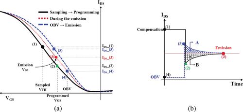
Figure 1. Schematic I-V characteristic of p-type TFT: The solid black line is the I-V curve when changing from VTH sampling to data programming period, and the dotted blue line is the I-V curve during the emission period.
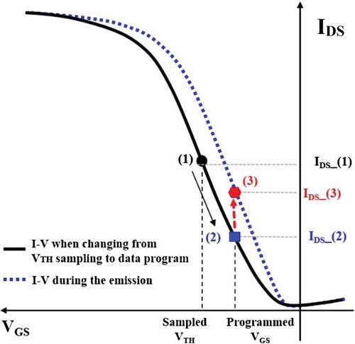
First step (VTH sampling): The solid black line in Figure represents the D-TFT I-V curve during the VTH sampling and programming period. The VTH [point (1)] is sampled at this time, and VGS [point (2)] is programmed based on the sampled VTH and data voltage (VDATA). Therefore, emission begins with desired OLED current IDS_(2), providing the desired luminance.
Second step (emission period): Figure shows that after VDATA programming, stress applied to the D-TFT changes the TFT I-V characteristics from IDS_(2) to IDS_(3) because of D-TFT hysteresis, changing the luminance. The transient luminance change caused by D-TFT hysteresis does not create a visible flicker at conventional frame rates (e.g. 60 Hz) because the perceived luminance fluctuation is well below the flicker fusion threshold [Citation22]. Under low-frame rate driving, however, it is critical to minimize the luminance fluctuation over time because the sensitivity of humans to flicker increases greatly from 10 to 15 Hz [Citation23]. As might be expected, the larger the hysteresis, the greater the luminance fluctuation and the more perceptible the flicker under low-frame rate driving. For this reason, low-frame rate driving requires that the leakage currents of the switching TFTs are low, and the hysteresis of the D-TFT is small. However, hysteresis is an intrinsic feature of an LTPS TFT [Citation24]. Therefore, for low-frame rate driving of an LTPO TFT-based AMOLED display, a new driving scheme that can compensate for D-TFT hysteresis is required.
In this paper, we propose a novel pixel circuit extending tCOMP without affecting the frame rate. Extension of tCOMP for each row guarantees accurate detection of VTH variations in D-TFTs. Also, the proposed driving scheme can compensate for the hysteresis of D-TFTs and supports low-frame rate flicker-free driving. Simulations were conducted, and a 6.0-inch quad high-definition (QHD) LTPO based AMOLED display was fabricated to verify the new pixel circuit and driving scheme. The manufactured AMOLED display exhibited excellent image quality during high-frame rate driving and no visible artifacts during low-frame rate driving.
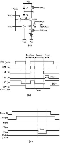
Figure 2. (a) Proposed pixel circuit and its timing diagrams of control signals in (b) refresh frame and (c) skip frame.
2. Operation of the proposed pixel circuit
Figure (a) illustrates the proposed pixel circuit composed of one D-TFT, five switching TFTs, and two capacitors. Figure (b) and (c) present the timing diagrams of the control signals for the refresh and skip frames, respectively. The refresh and skip frames constitute one frame during low-frame rate driving [Citation25]. Data are sequentially noted during the refresh frame period; no data are written during the skip frame period. DV(n), a dynamic voltage, provides the initialization voltage (VINT) and on-bias voltage (OBV) for hysteresis compensation to the refresh and skip frames, respectively. The OBV is always higher than VDATA. During the skip frame period, the S1 and S2 gate drivers output low voltage, and the clocks do not toggle; this reduces the power consumption of gate drivers. OBV is applied to the D-TFT to compensate for hysteresis during the skip frame period. Of the five switching TFTs, T1 and T2 are oxide TFTs, which is important because the gate voltage (VG) of the D-TFT changes, and the flicker degrades the image quality if the leakage current of the switching TFT connected to the gate of the D-TFT is large. Figure displays the proposed pixel circuit operation divided into six stages.
Figure (a) shows the anode reset stage (tA/R), where S3(n) and EM(n−1) are under low voltage and turn on T3 and T5. This stage aims to improve the low gray non-uniformity [Citation26]. VINT is equal to VSS or less than the OLED turn-on voltage to prevent current flow through the OLED when a black image is required.
Figure 3. Schematic of pixel circuit operation in (a) anode reset (tA/R), (b) initialization (tINT), (c) compensation (tCOMP), (d) data program (tPROG), (e) emission, and (f) tOBV in skip frame period.
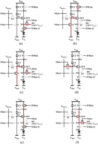
Figure (b) demonstrates the initialization stage (tINT), where S1(n) is under high voltage to turn on T1, and EM(n) is under low voltage to turn on T4. The S2(n) voltage is low to turn off T2, and the S3(n) and EM(n−1) voltages are high to turn off T3 and T5. This stage initializes the voltages of the gate and source nodes of the D-TFT. The gate node (N2) and source node (N1) of D-TFT are initialized to VREF and VDD, respectively. As T5 is turned off during the initialization stage, the OLED is completely off and achieves the real black luminance.
Figure (c) details the compensation stage (tCOMP), where the EM(n) goes high to turn off T4. The S1(n) voltage remains high to apply VREF to N2. S3(n) goes low to turn on T3. VGS_D-TFT is larger than |VTH_D-TFT|; the D-TFT begins to generate a current. Meanwhile, N1 discharges through T3 until the D-TFT is cut off. Finally, N1 discharges to VREF + |VTH_D-TFT|, as follows:
(1)
(1)
In this stage, S2(n) remains low to turn off T2, so the proposed compensation scheme does not require any voltage from the data lines. Therefore, the tCOMP of VTH is not limited by tSCAN, and the tCOMP values of multiple rows can overlap, as shown in Figure . This increases the total tCOMP available for sensing VTH_D-TFT and thus improves the precision of sensing. Hence, the pixel circuits maintain the D-TFT drain currents (IDS) uniform because the VTH variations of the D-TFT are well-compensated. The proposed pixel circuit generates a uniform driving current even during high-frame rate driving. So, this pixel circuit can improve the motion image quality of displays. In addition, T5 is turned off, and VINT is smaller than VSS; thus, all currents generated by the D-TFT flow into the DV line rather than the OLED. The OLED remains completely dark.
Figure 4. The extended tCOMP using overlapping scheme when (a) tCOMP is 2H and (b) tCOMP is 4H.
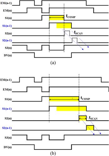
Figure (d) shows the data programming stage (tPROG) in which S2(n) is high to turn on T2, and VDATA is applied to N2. VDATA is stored in a capacitor (C1), and the source voltage of the D-TFT is boosted as follows:
(2)
(2) where VS is the source voltage of the D-TFT, and VREF is the reference voltage.
Figure (e) exhibits the emission stage, where S1(n) and S2(n) go low to turn off T1 and T2. EM(n) and EM(n−1) go low to turn on T4 and T5; thus, and VDD is applied to N1. The VG of the D-TFT is boosted as follows:
(3)
(3) where VG is the gate voltage of the D-TFT. The OLEDs of all pixels in a row begin to emit. The OLED current (IOLED) is:
(4)
(4) where
is the µ·COX·W/L of the D-TFT. In Eq. (4), VTH_D-TFT and VDD are eliminated; D-TFT VTH variations and I-R drop since the resistance of the VDD metal line will not influence the uniformity of the display image. Therefore, the proposed pixel circuit generates a uniform driving current, and the tCOMP of VTH is not limited by tSCAN.
Figure 5. Schematic of the dynamic behavior of the D-TFT due to the hysteresis characteristics: (a) I-V curve (dotted red line) during emission and (dotted blue line) during OBV and (b) schematic of IDS change before and after OBV.
In the hysteresis compensation stage (tOBV), OBV is applied during the skip frame period to compensate for D-TFT hysteresis and minimize flicker. Figure (f) points out that in this stage, S3(n) goes low to turn on T3; OBV is applied to N1 via N3. The OBV is higher than N2 and the programmed VDATA. OBV time (tOBV) is 50 µs. Thus, the VGS of the D-TFT remains on status. The mechanism of the proposed driving scheme’s hysteresis compensation can be described as follows:
After VTH sampling and VDATA programming, bias stress is applied to the D-TFT to change the VTH, resulting in the luminance fluctuations, as shown in Figure . IDS shifts from point (2) on the thick solid black line to point (3) on the thin dotted red line, as shown in Figure (a) and is shown on the time axis of the solid black line in Figure (b). To compensate for D-TFT hysteresis, OBV is applied to the D-TFT during the skip frame. This shifts IDS_(3) to IDS_(4), while VTH_D-TFT shifts positively. The voltage applied to the D-TFT changes the TFT I-V curve from the thin dotted red line to the thick dotted blue line. After OBV application, a bias stress opposite to that during programming and VTH sampling is applied to the D-TFT; the TFT I-V curve then moves from point (4) to point (5) along the thick dotted blue line in Figure (a). This is explained by the time axis, as shown in the blue dotted line in Figure (b). Therefore, the current increase from point (2) to point (3) after programming and VTH sampling is offset by the current drop from point (5) to point (3) after applying the OBV, thereby reducing the current change. Thus, flicker is not perceived during low-frame rate driving. Applying the OBV during the skip frame reduces the deviation between the current-decrease area (A: blue slanted area) after applying the OBV and the current-increase area (B: black mesh).
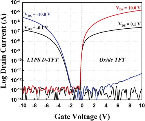
Figure 6. I-V characteristics of fabricated LTPS D-TFT and oxide switching TFT.
3. Results and discussion
SmartSpice (Silvaco Inc.) simulations were conducted, and a 6.0-inch QHD LTPO-based AMOLED display was fabricated to confirm that the proposed pixel circuit provided uniform luminance at 120 Hz and QHD resolution. The frame rate ranges from 1 to 120 Hz VRR driving. Although most smartphones still use full high-definition (FHD) resolution, the newest premium smartphones provide QHD (or even higher) resolution. Mobile devices with frame rates of 120 Hz are not yet widely available, especially mobile LTPO-based AMOLED displays.
The researchers simulated the proposed pixel circuit with QHD and a maximum frame rate of 120 Hz for future mobile applications. Figure shows the I-V characteristics of fabricated LTPS D-TFTs, with aspect ratios of 3.0 µm / 16.0 µm and oxide TFTs, with 3.0 µm / 3.5 µm aspect ratios, as used in the simulations. Table lists the parameters of the fabricated TFTs employed in simulations. Table outlines the capacitance, scan signals, and voltage levels simulated.
Table 1. Parameters of the fabricated LTPS and oxide TFT.
Table 2. Simulation conditions
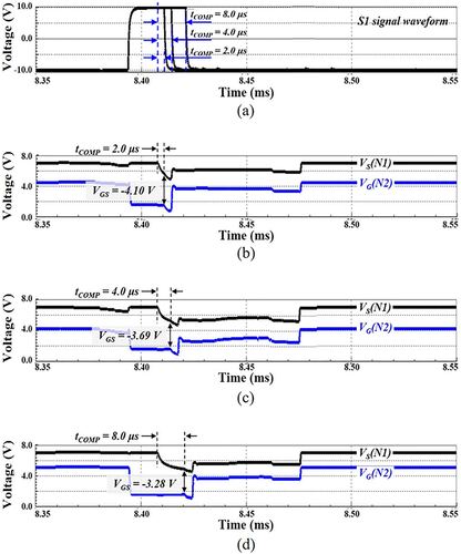
Figure 7. Simulated transient waveforms of the gate (N2) and source node (N1) of D-TFT according to tCOMP; (a) Input waveforms of S1 according to tCOMP, and VGS of D-TFT waveforms when tCOMP is (b) 2.0, (c) 4.0, and (d) 8.0 µs.
3.1. Compensation performance during high-frame rate
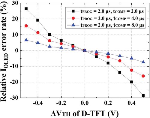
Figure (a) shows the input signal waveform of the S1 gate driver as tCOMP is varied from 2.0 µs to 8.0 µs. Figure (b) to (d) show the simulation results when D-TFT VG (N2) and VS (N1) change at tCOMP value of 2.0 µs, 4.0 µs, and 8.0 µs, respectively. At this time, tPROG is fixed at 2.0 µs. In a conventional driving scheme, tPROG and tCOMP are identical; the tCOMP values of FHD and ultra-high-definition (UHD) at 120 Hz frame rate are 8.0 µs and 2.0 µs, respectively. When tCOMP is 2.0 µs and 4.0 µs, the VGS values of the D-TFT are −4.10 V and −3.69 V after D-TFT VTH sensing, as shown in Figure (b) to (c), respectively. When tCOMP is 8.0 µs, the D-TFT VGS is −3.28 V, as shown in Figure (d). As the simulated D-TFT VGS is −3.18 V, with longer tCOMP, the D-TFT VGS becomes more similar to VTH. As tCOMP becomes longer, VGS converges to the D-TFT VTH. From these simulation results, the longer tCOMP allows more precise sensing of D-TFT VTH variations. Figure shows the relative IOLED error rates versus the D-TFT VTH variations of −3.0 V ± 0.1 V ∼ ± 0.5 V at 5 gray (0.2 nits) corresponding with different tCOMP. The relative IOLED error rate ranges from −28.6% to 26.4%, −16.2% to 15.6%, and −6.2% to 6.6% for tCOMP of 2.0, 4.0, and 8.0 µs, respectively, confirming that the proposed pixel circuit with the longest tCOMP of 8.0 µs indeed compensates more effectively for the D-TFT VTH variations. Also, the pixel circuit can freely extend tCOMP owing to its overlapping compensation scheme. The luminance uniformity of the manufactured 6.0-inch LTPO-based AMOLED display was measured to evaluate the compensation performance of the pixel circuit with various tCOMP values. Figure (a) to (c) present the optical images when tCOMP was 2.0, 4.0, and 8.0 µs, respectively. As tCOMP increases, the luminance uniformity improves. An ultra-high-resolution camera (RADIANT SOLUTION FPiSTM) was used to quantify uniformity. The measured luminance was 0.2 nits at 5,000 points within the panel. As a result of measuring local luminance uniformity, the standard deviations of luminance became smaller as tCOMP became longer (0.056, 0.024, and 0.008 for tCOMP values of 2.0, 4.0, and 8.0 µs, respectively), as shown in Figure (d) to (f). These results confirm that the simulation results provide accuracy for the measurement results of luminance uniformity. Since the proposed pixel circuit can increase the tCOMP, even if tPROG (or tSCAN) is short as the frame rate increases, the compensation performance can secure the same level as the FHD panel because the tCOMP of FHD is 8.0 µs. Therefore, the proposed pixel circuit ensures excellent luminance uniformity even at 120 Hz QHD high-frame rate driving. Also, as the pixel circuit can be driven at 120 Hz, the moving image quality of the AMOLED display can be improved [Citation27–29].
3.2. Flicker characteristics of low-frame rate
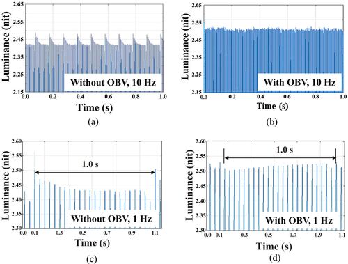
Since the lower the frame rate, the longer the skip frame period compared to that of high-frame-rate driving, the time to hold the programmed data also becomes longer. If the voltage-holding characteristic of the programmed data is poor during one frame, a flicker occurs. Therefore, the holding characteristics of VDATA are improved by applying oxide TFTs with very low leakage current to switching TFTs [Citation15]. Fig. S4(a) shows almost no luminance fluctuation at 120 Hz; flicker is not recognized. However, although the leakage current was reduced by using oxide TFT, luminance fluctuations were still present within one frame at a low gray level during 10 Hz driving. Consequently, flicker was perceived in panels fabricated from LTPO TFTs due to luminance drop at 10 Hz driving, as indicated in Figure (a). This luminance drop during the emission period is due to the D-TFT hysteresis. Figure explains the flicker mechanism, where the larger the D-TFT hysteresis, the greater the luminance change. Furthermore, flicker becomes more visible under low-frame rate driving [Citation23]. However, if the D-TFT hysteresis is small and settles rapidly, the magnitude and duration of luminance fluctuation are reduced, and flicker is less perceivable. Therefore, it is essential to minimize hysteresis to support low-frame rate driving. The proposed new driving scheme can compensate for D-TFT hysteresis. Figure (a) demonstrates the low-frame rate driving, divided into refresh and skip frames. Although no data are programmed during the skip frame, the OLED emits light. As highlighted in Figure (a), the proposed driving method supports flicker-free display low-frame rate driving; the OBV applied to the D-TFT during the skip frame compensates for hysteresis as follows. The D-TFT VTH positively shifts after OBV is applied during the skip frame. A negative shift of the D-TFT VTH during the refresh frame, and a skip frame with OBV, can be compensated for by the OBV. Figure (b) shows the D-TFT VTH behavior when OBV is applied during the skip frame period. Simulations were conducted to verify the proposed driving scheme. Figure (a) exhibits the simulation result that D-TFT VTH is negatively shifted because of hysteresis during the skip frame period when OBV is not applied when driving at 10 Hz. Figure (b) also shows the simulation result that D-TFT VTH is positively shifted during the skip frame period when OBV is applied during driving at 10 Hz. From the simulation results, if OBV is applied in the skip frame period, the negative shift of D-TFT VTH is reduced due to the relatively positive shift of D-TFT VTH. Figure (c) reflects the simulation result that IOLED changes when OBV is not applied during 10 Hz driving. As in Figure (a), D-TFT VTH fluctuation increases, as does the IOLED change. Figure (b) reveals that when OBV is applied, the fluctuation of D-TFT VTH’ is decreased, as is the IOLED change, as shown in Figure (d). Same as the 10 Hz simulations, the simulations were performed at 1 Hz depending on whether OBV was applied or not. Figure (a)-(b) explains that D-TFT VTH is negatively shifted during the skip frame period when OBV is not applied but not when OBV is applied when driving 1 Hz. From the simulation results, if OBV is applied during the skip frame period, the negative shift of D-TFT VTH is reduced by a relatively positive shift in D-TFT VTH. Figure (c) confirms IOLED changes when OBV is not applied during 1 Hz driving. Figure (a)’s results suggest that when OBV is not applied, the fluctuation of D-TFT VTH is increased, and the IOLED change also increases, as shown in Figure (c). Figure (b)’s results imply that when OBV is applied, the fluctuation of D-TFT VTH is decreased, and the IOLED change also decreases, as shown in Figure (d). Therefore, the OBV driving scheme is essential for the LTPO pixel circuit that can control the VTH behavior of D-TFT. A 6.0-inch QHD LTPO-based AMOLED display is fabricated to verify the proposed pixel circuit and new driving scheme, and luminance measurements were performed with the MINOLTA CA-410. Figure (a) and (b) show the measurement results of luminance fluctuation without and with OBV during 10 Hz driving, respectively. Figure (a) presents that if OBV was not applied, the luminance fluctuation was 3.0% between frames. Such luminance fluctuation causes visible artifacts, that is, flicker. However, when OBV was applied, the luminance fluctuation was 0.5%. Figure (c) and (d) show the measurement results without and with OBV during 1 Hz driving, respectively. Figure (c) represents that when OBV was not applied, the luminance fluctuation was 2.8% between frames. When OBV is applied, the luminance fluctuation was 1.0%. Therefore, no visible artifacts are perceived, and flicker is not recognized. Figure conveys that the measurement results are consistent with those of the simulation. Based on these results, Figure shows the results of flicker measurement when OBV is applied and not applied using the FLICKER MODE of MINOLTA CA-410. During 10 Hz driving, the flicker was −15 dB when no OBV was applied; this value is highly perceptible. However, when OBV was applied, both 1 Hz and 10 Hz driving showed the flicker was no higher than −50 dB, and no artifacts were perceived. These results proved that the causes of flicker of LTPO-based AMOLED pixel circuit in the low-frame rate driving are the leakage current of the switching TFTs and D-TFT hysteresis. Also, it is proved that the proposed compensation pixel circuit and driving scheme operate stably at high- and low-frame rates, so full VRR driving can be implemented. Figure shows the measurement result of power consumption according to frame rate. The condition of power consumption measurement is 40% turn-on at 500 nits with a 6.0-inch QHD panel. The power consumption decreases as the frame rate decreases, and when driving at 1 Hz, the power consumption of the driver IC block (including analog and logic) is reduced by a quarter compared to that of the 120 Hz frame rate driving. The reason for the reduction in power consumption is that output signals of data and some gate drivers are not operated during the skip frame period when driving at a low-frame rate, as indicated in Figure (a). However, the power consumption of the panel does not decrease because the frame rate does not affect the D-TFT current. Based on the measurement results, the LTPO-based AMOLED display provides excellent moving image quality and low power consumption through the VRR driving depending on the operation environment(e.g. game, AOD, still image, and text mode).
Figure 8. Simulated relative IOLED error rates at ΔVTH_D-TFT = ±0.1 V, ± 0.2 V, ± 0.3 V, ± 0.4 V, ± 0.5 V according to tCOMP; tCOMP is 2.0, 4.0, and 8.0 µs.
4. Comparison to previous works
Table compares the new pixel circuit with previous ones. The circuits in [Citation2,Citation6,Citation30,Citation31] have tCOMP values larger than the tSCAN values. However, the pixel circuits in [Citation2,Citation6], and [Citation32] cannot compensate for VDD IR drop, so they cause upper and lower luminance deviation in the display panel. The pixel circuit of [Citation30] lacks high-resolution capability because it requires two data lines. Also, none of these circuits compensates for hysteresis. They cannot operate at low-frame rates as they are composed only of LTPS TFTs. Pixel circuits based on LTPO [Citation32,Citation33] do not compensate for hysteresis and cannot extend the tCOMP. Therefore, even with LTPO pixel circuits, a flicker occurs during low-frame-rate driving, and compensation performance deteriorates due to the reduced tCOMP during high-frame-rate driving. The proposed pixel circuit and driving scheme can achieve VRR driving from 1 to 120 Hz.
Figure 9. The optical image of a 6.0-inch LTPO-based AMOLED display when tCOMP is (a) 2.0, (b) 4.0, and (c) 8.0 µs, and measured luminance uniformity of 100 × 50 pixels area when tCOMP is (d) 2.0, (e) 4.0, and (f) 8.0 µs.
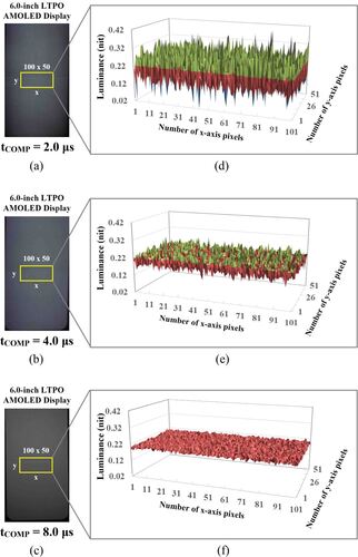
Figure 10. The conceptual schematic of (a) timing diagram of the OBV driving at low-frame rate and the (b) VTH behavior of D-TFT when OBV is applied.
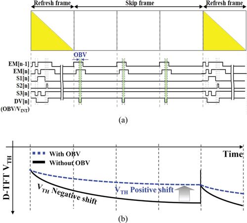
Figure 11. Simulation results of D-TFT VTH behavior and IOLED fluctuation according to the OBV at 10 Hz: (a) D-TFT VTH behavior without OBV, (b) D-TFT VTH behavior with OBV, (c) IOLED variation without OBV during skip frame, and (d) IOLED variation with OBV during skip frame.
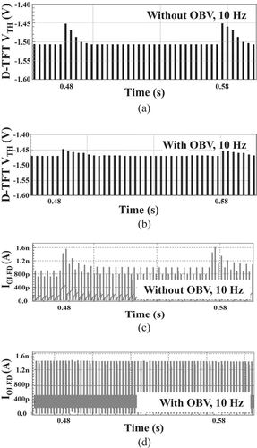
Figure 12. Simulation results of D-TFT VTH behavior and IOLED fluctuation according to the OBV at 1 Hz (a) D-TFT VTH behavior without OBV, (b) D-TFT VTH behavior with OBV, (c) IOLED variation without OBV during skip frame, and (d) IOLED variation with OBV during skip frame.
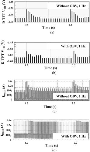
Figure 13. Measurement results of luminance fluctuation (a) without OBV at 10 Hz, (b) with OBV at 10 Hz, (c) without OBV at 1 Hz, and (d) with OBV at 1 Hz.
5. Conclusion
This paper presents a novel pixel circuit and driving scheme based on an LTPO TFT backplane. This extends the tCOMP. The pixel circuit overlaps the tCOMP of multiple rows, which increases the VTH sensing time and allows precise extraction of D-TFT VTH variations. A novel pixel driving scheme that compensates for the hysteresis by applying OBV to the D- TFT was proposed and experimented to ensure flicker-free display during low-frame rate driving. A 6.0-inch QHD LTPO-based AMOLED panel is fabricated, and the fabricated panel exhibits excellent luminance uniformity. Measurement results of luminance uniformity of the proposed pixel circuit show that the standard deviation of luminance was reduced from 0.056 to 0.008 by extending the tCOMP from 2 to 8 µs. The proposed pixel circuit exhibits excellent compensation performance of D-TFT VTH variations even during high-frame-rate driving with a short tSCAN. Also, applying OBV to the D-TFT greatly reduces flicker at 1 and 10 Hz. The flicker level was –51 dB, without any visual artifacts, during 1 Hz driving. Compared to 120 Hz, the power consumption of the driver IC is reduced by a quarter at 1 Hz. Therefore, the proposed pixel circuit and driving scheme based on the LTPO TFT backplane can operate without visual artifact in VRR driving from 1 to 120 Hz and can be used in the LTPO-based AMOLED display for mobile devices.
Figure 14. Flicker measurement results without and with OBV according to the frame rate.
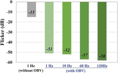
Figure 15. Measurement results of power consumption according to the frame rate.
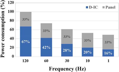
Table 3. Comparison of the proposed pixel circuit and other works.
Supplemental Material
Download MS Word (1.2 MB)Disclosure statement
No potential conflict of interest was reported by the author(s).
Additional information
Funding
Notes on contributors

Jung Chul Kim
Jung Chul Kim received the M.S. degree from the Department of Information Display, Kyung Hee University, Seoul, South Korea, in 2003. He is currently pursuing his Ph.D. degree at the School of Electrical and Electronic Engineering, Yonsei University, Seoul, South Korea. He is also currently a Research Fellow on mobile OLED panel design with the Mobile Business Unit, LG Display, Paju, Korea. His current research interests include the OLED compensation pixel circuit and advanced technology of flexible display panel.

I. Sak Lee
I. Sak Lee received his Ph.D. degree from the School of Electrical and Electronic Engineering, Yonsei University, Seoul, South Korea, in 2022. He is also a Senior Research Engineer in the OLED panel devices development team with the TV Business Unit, LG Display, Paju, Korea. He has been researching high-performance n-type oxide TFTs and their application to phototransistors.

Hyung Tae Kim
Hyung Tae Kim received his B.S. degree from the Department of Electronic Engineering, Chung-Ang University, Seoul, South Korea, in 2018. He is also currently a Ph.D. candidate at the School of Electrical and Electronic Engineering at Yonsei University, Seoul, South Korea. He has been researching an application based on oxide TFTs, including neuromorphic devices and photosensors.

Jong Bin An
Jong Bin An received his B.S. degree from the School of Electrical and Electronic Engineering at Yonsei University, Seoul, South Korea, in 2020. He is currently a Ph.D. candidate at the same institute. He has been researching high-performance n-type oxide TFTs and their application to phototransistors.

Jae Sung Kim
Jae Sung Kim received his B.S. degree from the Department of Electrical Engineering, Kyung Hee University, Gyeonggi-do, South Korea, in 2010. He is also a Senior Research Engineer in mobile OLED panel design with the Mobile Business Unit, LG Display, Paju, Korea. His current research interests include the OLED compensation pixel circuit.

Juhn Suk Yoo
Juhn Suk Yoo received his M.S. and Ph.D. degrees from the School of Electrical and Electronic Engineering, Seoul National University, Seoul, South Korea, in 1997 and 2001, respectively. He is currently a Chief Research Fellow of the Mobile Business Unit, LG Display, Paju, Korea. His research interests are LTPS and oxide TFT for AMOLED mobile display applications. He is also interested in advanced technology of flexible display panel.

Han Wook Hwang
Han Wook Hwang received his Ph.D. degree from the School of Electrical and Electronic Engineering, Yonsei University, Seoul, South Korea, in 2019. He is currently a Vice President of the Mobile Business Unit, LG Display, Paju, Korea. His research interests are LTPS and oxide TFT for AMOLED mobile display applications. He is also interested in the development of flexible display applied with AMOLED.

Hyun Chul Choi
Hyun Chul Choi received his M.S. and Ph.D. degrees from the Department of Chemistry, Korea Advanced Institute of Science and Technology (KAIST), Daejeon, South Korea, in 1991 and 1994, respectively. He is currently a Senior Vice President of the Mobile Business Unit, LG Display, Paju, Korea.

Yong Min Ha
Yong Min Ha received his M.S. and Ph.D. degrees from the Department of Electrical Engineering, Korea Advanced Institute of Science and Technology (KAIST), Daejeon, South Korea, in 1990 and 1994, respectively. He is currently an Executive Vice President of the Quality Management Center, LG Display, Paju, Korea.

Hyun Jae Kim
Hyun Jae Kim received his Ph.D. degree from the Department of Materials Science and Engineering, Columbia University, New York City, NY, USA, in 1996. Since 2005, he has been a Professor with the Faculty of the School of Electrical and Electronic Engineering, Yonsei University, Seoul, South Korea.
References
- G.B. Chaji, and A. Nathan, Low-power low-cost voltage-programmed a-Si:H AMOLED display for portable devices, J. Display Technol 4 (2), 233–237 (Jun. 2008).
- C.-L. Lin, et al., Compensation pixel circuit to improve image quality for mobile AMOLED displays, IEEE J. Solid-State Circuits 54 (2), 489–500 (Feb. 2019).
- R. Yonebayashi, et al., High refresh rate and low power consumption AMOLED panel using top-gate n-Oxide and p-LTPS TFTs, in SID Tech. Dig 51, 355–358 (2020).
- H.J. Luo, et al., Complementary LTPO technology, pixel circuit and integrated gate drivers for AMOLED displays supporting variable refresh rates, in SID Tech. Dig 50, 351–354 (2019).
- T.K. Chang, C.W. Lin, and S. Chang, LTPO TFT Technology for AMOLEDs, in SID Tech. Dig 50, 545–548 (2019).
- J.C. Kim, S.H. Hong, S.J. Jung, M.H. Shin, J.S. Yoo, H.W. Hwang, Y.M. Ha, and H.J. Kim, A novel OLED Pixel circuit with controllable threshold voltage compensation time, in IDW, 505–506 (2019).
- C.-L. Lin, C.-C. Hung, P.-S. Chen, P.-C. Lai, and M.-H. Cheng, New voltage-programmed AMOLED pixel circuit to compensate for nonuniformity electrical characteristics of LTPS TFTs and voltage drop in power line, IEEE Trans. Electron Devices 61 (7), 2454–2458 (Jun. 2014).
- J.P. Lee, H.S. Jeon, D.S. Moon, and B.S. Bae, Threshold voltage and IR drop compensation of an AMOLED pixel circuit without a VDD line, IEEE Electron Device Lett 35 (1), 72–74 (Jan. 2014).
- C.-H. Ho, C. Lu, and K. Roy, An enhanced voltage programmed pixel circuit for compensation GB-induced variations in poly-Si TFTs for AMOLED displays, J. Display Technol 10 (5), 345–351 (May 2014).
- W.-J. Wu, L. Zhou, M. Xu, L.-R. Zhang, R.-H. Yao, and J.-B. Peng, An AC driving pixel circuit compensating for TFTs threshold-voltage shift and OLED degradation for AMOLED, J. Display Technol 9 (7), 572–576 (Jul. 2013).
- Y. Kim, J. Kanicki, and H. Lee, An a-InGaZnO TFT pixel circuit compensating threshold voltage and mobility variations in AMOLEDs, J. Display Technol 10 (5), 402–406 (Jun. 2013).
- G.B. Chaji, and A. Nathan, Parallel addressing scheme for voltage-programmed active-matrix OLED displays, IEEE Trans. Electron Devices 54 (5), 1095–1100 (May 2007).
- Y.H. Hong, E.K. Jung, H. Im, and Y.S. Kim, Improvement of the low gray-level expression using hybrid pulse width modulation and pulse amplitude modulation driving method for a micro light-emitting diode pixel circuit,” J, Information Display 22 (4), 243–249 (2022).
- N.-H. Keum, K. Oh, S.-K. Hong, and O.-K. Kwon, A pixel structure using block emission driving method for high image quality in active-matrix organic light-emitting diode displays, J. Display Technol 12 (11), 1250–1256 (Nov. 2016).
- R.D. et al, A Novel De-Mux and 120 Hz Driving Technology for High Resolution OLED Displays, in SID Tech. Dig 49, 540–542 (2018).
- J.H. et al, Design for AMOLED Display with an Improved Uniformity and a Smaller Bezel, in SID Tech. Dig 42, 1132–1135 (2011).
- U.J. Chung, et al., Manufacturing technology of LTPO TFT, in SID Tech. Dig 51, 192–195 (2020).
- P.-T. Lee, Y.-S. Lin, and C.-L. Lin, Compensation pixel circuit based on LTPS TFTs to improve effect of leakage current for AMOLED displays with low-frame rate, in AM-FPD, 107–110 (2020).
- R. Yonebayashi, et al., High refresh rate and low power consumption AMOLED panel using top-gate n-Oxide and p-LTPS TFTs, in SID Tech. Dig 51, 355–358 (2020).
- H.J. Luo, et al., Complementary LTPO technology, pixel circuit and integrated gate drivers for AMOLED displays supporting variable refresh rates, in SID Tech. Dig 50, 351–354 (2019).
- H.J. Chung, D.H. Kim, and B.K. Kim, Hysteresis characteristics in low temperature poly-Si thin film transistor, J. Information Display, 6 (4), 6–10 (Jun. 2005).
- C. Landis, Determinants of the critical flicker-fusion threshold, Phys. Rev, 34 (2), 259–286 (May 1954).
- D.H. Kelly, Visual Responses to Time-Dependent stimuli. I. Amplitude sensitivity measurements, J. The Opt. America 51 (4), 422–429 (Apr. 1961).
- H.W. Hwang, Study on recoverable residual image phenomenon of plastic OLED display., Doctoral thesis, Yonsei Univ, Korea, Feb. 2020.
- D.S. Oh, et al., Low Frequency Driving Display to Reduce Logic Power in Liquid Crystal Display, in SID Tech. Dig 45, 1199–1202 (2014).
- S.H. Na, W.K. Min, D.Y. Kim, H.W. Hwang, Y.H. Ha, and H.J. Kim, Enhancement of picture quality on ultra-low brightness by optimizing the electrical potential required for OLED charging in the AMOLED displays, J. Information Display 22 (4), 1–10 (May 2021).
- H.-W. Chen, J.-H. Lee, B.-Y. Lee, S. Chen, and S.-T. Wu, Liquid crystal display and organic light-emitting diode display: present status and future perspectives, Light: Science & Application 7, 1–13 (2018).
- T. Kurita, A. Saito, and I. Yuyama, Consideration on perceived MTF of hold type display for moving images, in IDW, 823–826 (1998).
- T. Kurita, Moving picture quality improvement for hold-type AM-LCDs, in SID Tech. Dig 32, 986–989 (2001).
- J. Huh, S.W. Wang, G.H. Cho, Y.J. Park, and J.C. Kim, Design for AMOLED Display with an improved uniformity and a smaller bezel, in SID Tech. Dig 42, 1132–1135 (2011).
- N.H. Keum, S.K. Hong, and O.K. Kwon, An AMOLED Pixel circuit with a compensating scheme for variations in subthreshold slope and threshold voltage of driving TFTs, IEEE J. Solid-State Circuits 55 (11), 3087–3096 (Nov. 2020).
- R. Yonebayashi, et al., High refresh rate and low power consumption AMOLED panel using top-gate n-Oxide and p-LTPS TFTs, in SID Tech. Dig 51, 355–358 (2020).
- H.J. Luo, et al., Complementary LTPO technology, pixel circuit and integrated gate drivers for AMOLED displays supporting variable refresh rates, in SID Tech. Dig 50, 351–354 (2019).