
 ?Mathematical formulae have been encoded as MathML and are displayed in this HTML version using MathJax in order to improve their display. Uncheck the box to turn MathJax off. This feature requires Javascript. Click on a formula to zoom.
Abstract
This review aims to provide a technical roadmap and an overview of recent progress in the development of backplane thin film transistors (TFTs) for organic light-emitting diodes flat panel displays and next-generation flexible displays. In the introduction, we provide a general overview of the research trends for backplane TFTs. The main part describes the current technical level and prospects for amorphous metal oxide semiconducting, metal halide perovskites, and 2D transition metal dichalcogenides TFTs. The summary and prospects are provided in the conclusion section.
1. Introduction
Optimizing materials and manufacturing processes for backplane thin film transistors (TFTs) has been crucial in advancing and enhancing Flat Panel Displays (FPDs). TFTs are the fundamental building blocks of FPDs, controlling current flow and operating the display pixels. In the past, TFTs made of amorphous silicon (a-Si) were used in backplane circuits in liquid crystal displays. However, these TFTs were limited in their application to organic light-emitting diode (OLED) displays. New TFT technologies were needed to support higher current values and stable operation. Low-temperature polycrystalline silicon (LTPS) TFTs were developed and successfully used in OLED displays to meet these requirements. Despite these advances, high-power consumption and poor performance uniformity over large areas remained the limitations of using LTPS TFTs in large-area display applications such as OLED TVs [Citation1–5].
Amorphous metal oxide semiconductors, such as indium gallium zinc oxide (IGZO), are widely used as OLED driving circuits due to their cheap manufacturing cost, high-performance uniformity, and low off-state current [Citation6]. However, the low mobility of these transistors needs to be improved for scaling up to high-resolution displays. One solution to this challenge is LTPO technology, which combines the advantages of metal oxide and LTPS TFTs. However, LTPO technology has a slightly more complicated manufacturing process and higher process cost than the existing technology that implements a backplane with one transistor type. Therefore, further improvements in the performance of oxide transistors are necessary to overcome this problem.
Perovskite and 2D transition metal dichalcogenides (TMDCs) materials are emerging semiconducting materials for a channel of TFTs, offering several advantages over traditional TFT materials, including high carrier mobility, low power consumption, and improved operational stability. Although perovskite and TMDCs TFTs are still in the early stages of development, they need to improve various aspects of performance, including processability and stability. Despite their potential, material toxicity, device hysteresis, and perovskite material stability are major challenges that need to be overcome for commercialization on a wide scale [Citation7]. 2D TMDCs channel can be uniformly affected by the gate voltage, confining all electrons in an atomically thin layer. However, contact resistance (Rc) caused by defects of the TMDC surface in the conventional metal electrode formation process is a main challenge for TMDCs transistors [Citation8]. In addition, the lack of a process to achieve uniform device performance over a large area, such as in display, also needs to be overcome. Various attempts are being made to improve the perovskite’s stability and reliability and TMDCs TFTs’ contact resistance, and it is expected that they could become a viable option for use in FPDs in the future.
This review provides recent progress in the development of backplane TFTs for flat panel displays and next-generation displays, such as flexible and rollable mobile phones or TVs. This article introduces various research efforts to improve the mobility and stability of n-type oxide TFTs and the recent research development based on perovskite and 2D TMDC materials. The purpose is to provide an overview of the direction of the new materials and their potential to enhance performance.
2. Metal oxide TFTs
Since binary oxide semiconductor materials, including SnO2 and In2O3, were introduced as channel layers of TFTs in 1964 [Citation9], research on oxide semiconductors has led to the development of multi-component oxide semiconductors such as In-Ga-Zn-O with various advantages. Up to now, amorphous metal oxide semiconductor-based TFTs have drawn considerable attention due to their many advantages, such as high mobility compared to a-Si, transparency, and large area uniformity [Citation10]. Based on these characteristics, research related to this section has been conducted to achieve higher mobility and excellent stability for application to high-end displays with a large area, high resolution and high PPI.
In this regard, the research summary of n-type oxide TFTs (Table , Figure ) is organized in the following parts: (1) modification of metal chemical composition by atomic layer deposition (ALD) process; (2) high-performance TFTs through induction of crystallization; and (3) mobility enhancement effect of various metal capping layers. In addition, research for the realization of high-performance p-type oxide TFTs (Table ) is discussed.
Figure 1. Field-effect mobility trends depending on the process temperature of various thin-film transistors.
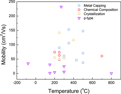
Table 1. Recent representative research of n-type metal oxide-based TFTs.
Table 2. Recent representative research of p-type metal oxide-based TFTs.
Among the various deposition methods of oxide semiconductors, the atomic layer deposition (ALD) process has been attracted significant attention to the deposit of high-quality thin films based on the self-limited chemical reaction between the precursor and the reactant. This method allows easy tuning of the chemical composition, microstructure, and electrical properties, along with excellent step coverage and thickness controllability. According to these advantages, many types of oxide TFTs using the ALD process have high field-effect mobility (20 ≤ μFE ≤ 80).
Recent research on ALD-proceed oxide TFTs has reported excellent performance with high mobility and stability by cation composition control. The chemical composition is precisely controlled at the atomic layer level. For example, high mobility properties can be achieved by controlling the subcycle and dosing time of indium-based metal precursors [Citation11–15]. Although the ALD-based process has some drawbacks, such as a slow deposition rate, it presents the feasibility of high-performance devices with complicated 3-dimension structures.
It is a well-known fact that improvement in crystallinity leads to improvement in device mobility. However, the crystallization process requires high temperature, which is unsuitable for glass substrates for display industries or plastic substrates that show low glass transition temperature. Recently, many studies on low-temperature crystallization have been conducted to improve mobility. Shin et al. report the crystallization of IGZO via a tantalum catalytic layer [Citation12]. The Ta layer releases electrons into the underlying IGZO layer, breaking the weak M-O bond. Crystallization occurs during the rearrangement or diffusion of broken M-O bonds during annealing. Attempts have been made to control crystallization by adding hydrogen during deposition [Citation13,Citation14]. By adding hydrogen, crystallization of the oxide semiconductor during deposition can be suppressed by eliminating the nuclei density, and crystallization of oxide film during post-annealing can enlarge the grain size, thus improving mobility. Zn ions stabilize the amorphous network in oxide semiconductors represented by IGZO [Citation15,Citation16]. Accordingly, research on the crystallinity of oxide semiconductors without Zn has been reported. Park et al. detail the high-performance crystallized IGO TFT with a process temperature of 200 °C. By adjusting oxygen partial pressure, low-temperature crystallization is achieved, thus leading to the high mobility of 56 cm2/Vs. IGTO TFTs crystallized at 400 °C have also been reported showing high mobility of 116.5cm2/Vs.
Research on realizing high-performance oxide TFTs through structural modifications such as dual gate [Citation35], passivation [Citation36], and metal capping has been continuously proposed. Compared to other studies, the introduction of metal capping layers can improve the electrical performances of oxide TFTs with various mechanisms, such as electron injection [Citation19,Citation24], conductive region formation [Citation24], and removal of oxygen-related defect state [Citation21,Citation37].
Based on this mechanism, much research on metal-capped oxide TFTs achieved significant mobility enhancement effects (over 100 cm2/Vs) without degrading other transfer parameters. Additionally, this method-maintained device’s reliability has superior electrical performance. Recently, the mobility improvement effect of the metal capping layer was also observed in TFTs with a top-gate structure that is process-compatible with the industries to be applied to next-generation displays [Citation38].
Oxides have difficulty achieving high-performance p-type because carrier conduction mainly occurs in the valence band, formed from oxygen p asymmetrically localized orbitals, limiting carrier mobility. Recently, much attention has been given to SnO-, NiOx-, and CuOx-based transistors. Yen et al. claim that a 7 nm thick SnO exhibits field effect mobility of 4.4 cm2/Vs fabricated by the sputtering method with a low process temperature of 200 °C [Citation25]. Also, research on SnO deposition using atomic layer deposition (ALD) with the precursor of N,N′-tert-Butyl-1,1-dimethylethylenediamine stannylene (II) and reactant of deionized (DI) water has been reported. Here, a two-step crystallization process is introduced to grown c-axis oriented SnO and shows the mobility of ∼ 6 cm2/Vs [Citation26].
Copper oxide has two common forms: cuprous oxide or cuprite (Cu2O) and cupric oxide or tenorite (CuO). Both copper oxides are generally p-type semiconductors, and Cu2O shows higher mobility than CuO. By doping Ga, which presents high-oxygen affinity, the Cu2O film decreases oxygen vacancy (Vo) during the reduction [Citation27]. By reduction, Cu2O TFT improved overall TFT performance, such as field effect mobility, on/off ratio, threshold voltage, and subthreshold swing. Also, there are some reports about copper oxide TFT fabricated by ALD. Wanjoo et al. examine the CuOx TFT fabricated by the ALD process with the precursor of hexafluoroacetylacetonate Cu(I)(3,3-dimethyl-1-butene)[(hfac)Cu(I)(DMB)] and reactant of ozone gas (O3) [Citation28]. The XPS results indicate that the Cu2+ bonding state increases during the annealing temperature of 300 °C, which means the formation of Cu2O. Here, the mobility of CuOx TFT results in 5.64 cm2/Vs.
NiOx is a promising p-type material due to its good visible transparency, chemical stability, and electrical properties. Shan et al. reveal CuOx and NiOx TFTs fabricated by a solution process with various annealing temperatures, with optimum field effect mobility of 0.44 and 0.79 cm2/Vs, respectively. By replacing SiO2 to high-k Al2O3, NiOx TFTs exhibit high field effect mobility of 25 cm2/Vs [Citation29]. Yang et al. present Li-doped NiOx TFT fabricated with solution-based combustion synthesis and deep-UV treatment. By incorporating Li into the NiOx matrix, the film’s resistivity and carrier concentration were decreased and increased, respectively. The NiOx TFT with the optimal Li content exhibits a field effect mobility of 3 cm2/Vs, more than 5 times higher than the control NiOx TFT [Citation30]. Similarly, Liu et al. investigated Cu-doped NiOx, where Cu:NiO was fabricated by a solution combustion synthesis with an annealing temperature of 150 oC. Cu replaces the Ni sites and generates substituent defects, increasing the p-type conductivity. Optimum Cu:NiO TFTs display a field effect mobility of 1.53 cm2/Vs and an on/off ratio of ∼104 [Citation31].
Tellurium, a two-dimensional material, has recently been reported to have high hole mobility. In 2021, Zavabeti et al. studied β-TeO2 nanosheets TFT that exhibits high mobility of 232 cm2/Vs and an on/off ratio exceeding 106 [Citation32]. This is a higher value than conventional oxide transistors. Here, β-TeO2 and Te are considered promising p-type semiconducting materials. In 2020, Te TFTs fabricated by evaporation at -80 °C were reported [Citation33]. Thanks to the vacuum process, a 4-inch wafer scale was achieved, and TFTs showed high mobility of ∼35 cm2/Vs. Also, thanks to the low-temperature process, flexible TFTs on PET substrates were successfully demonstrated. Recently in 2022, Te TFT fabricated by sputtering was also explored [Citation34]. Here, TFT shows high mobility above 30 cm2/Vs and an on/off ratio of 5.8 × 10⁵ with a 4-inch wafer scale. Finally, the CMOS inverter was demonstrated utilizing IGZO and Te TFT, showing a high gain of ∼75.2.
Oxide semiconductors have been studied a lot since the report of IGZO by Nomura et al. Higher mobility is required to meet the demands of modern electronic devices. Unlike high-performance n-type oxide semiconductors with mobility of 100 cm2/Vs or more, securing high-mobility p-type oxide semiconductors is difficult due to localized oxygen 2p orbitals. Various methods have been tried to improve mobility, but the characteristics are still insufficient to be used in the actual backplane of the display, so it still needs to be improved.
3. Metal-halide perovskite TFTs
Metal–halide perovskites (MHPs) are drawing attention as excellent materials for optoelectronic devices, benefiting from their charge transport properties, unique defect tolerance characteristics, and tunable bandgap [Citation39]. Perovskites consist of ABX3 structure, in which BX6 octahedra are connected repeatedly in three dimensions, A site is a monovalent cation (MA+, FA+, Cs+), B site is a divalent cation (Pb2+, Sn2+), and X site is halide anion (Cl-, Br-, I-).
Perovskite can be categorized with many criteria (e.g. the existence of organic A cation, dimension of perovskite structure, B site cation, etc.). All the perovskite has pros and cons. The first perovskite TFT was composed of PEA2SnI4 [Citation40], a 2D Ruddlesden-Popper structure rather than the typical 3D perovskite structure of ABX3. In the case of 2D perovskite, it is slightly better in stability than 3D perovskite. When 3D perovskite is exposed to oxygen or moisture, Pb2+ and Sn2+ are easily oxidized to Pb4+ and Sn4+, respectively. However, in 2D perovskite, A cations between each octahedra layer act as a barrier toward oxygen penetration, resulting in relatively better stability [Citation41].
However, in terms of theoretical performance, 3D perovskite has higher carrier mobility than 2D perovskite because 2D perovskite has limited charge transport and a large bandgap [Citation42]. As a result, many studies on MAPbI3, which have high efficiency in solar cells, have been conducted [Citation43]. However, Pb perovskite has severe problems, such as toxicity and ion migration. The dominant iodide vacancy has a low migration barrier, so when the gate field is applied, vacancies move toward the field direction and balance out the gate field, which leads to performance degradation. Therefore, the performance of Pb perovskite can be confirmed only when low-temperature or pulsed mode measurement is used [Citation44].
As an alternative to Pb perovskite, Sn perovskite shows great potential. First, Sn is an eco-friendly material relative to Pb [Citation45] and has almost negligible ion migration [Citation46,Citation47]. The dominant vacancy of Sn perovskite is tin vacancy, which has a high migration barrier. Therefore, ion migration is almost negligible. Also, it has very high hole mobility, making it a very suitable material for high-performance transistors. Because of this, research on Sn perovskite is being conducted more actively than before.
In addition, a new structure called double perovskite is also being studied. The general formula is A2MIMIIIX6 (A is a monovalent cation, MI is a univalent metal, MIII is a trivalent metal, and X is a halide). In this structure, MIX6 and MIIIX6 octahedra were connected alternatively. Although it does not show high mobility, it has superior stability toward ambient environments and great potential [Citation48].
Various structures, new elements, and different compositions are adopted to raise the performance and stability of perovskite TFT (Figure , Table ). Still, tremendous novel ways are veiled. Although perovskite has rapidly grown over the last decade, stability and down-scaling have to be investigated further to apply them to commercial backplanes.
Figure 2. The field effect mobility trends of MHPs TFTs for different chemical compositions.
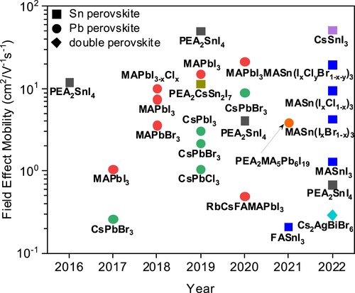
Table 3. Recent progress of MHPs TFTs.
4. 2d transition metal dichalcogenides TFTs
2D transition metal dichalcogenides (TMDCs) have high , high mechanical flexibility, and layer-dependent band structure that differs from their bulk counterparts. Researchers have studied these unique material properties for decades [Citation66,Citation67], making TMDCs a candidate for next-generation materials in various fields, including backplane transistors for display. MoS2 has attracted attention because it is readily available, and high-quality crystals can be easily obtained. MoS2 is also mechanically and chemically robust [Citation68]. However, TMDCs face difficulties in application due to factors such as high contact resistance (Rc), high subthreshold swing (SS), and Ion/Ioff ratio. In particular, contact resistance has a dominant impact on the performance of FET devices, and solving this is the most important area of research in TMDCs.
Various strategies have been adopted in the 2D TMDCs field to reduce contact resistance, including molecular doping [Citation69,Citation70], phase engineering [Citation71], graphene contact [Citation72,Citation73], edge contact [Citation74,Citation75], van der Waals contact [Citation76,Citation77], and semimetal interlayer contact [Citation78,Citation79]. Molecular doping is a simple and easily scalable method that has been extensively researched. Recently, thiol-based molecules have been found to provide the new tunneling path at the metal–semiconductor (MS) junction. This new tunneling path has lower energy barriers and exhibits Ohmic-contact behaviors, reducing Rc (to 25.2 kΩ·μm) [Citation69].
Additionally, by forming a junction between the edge of the TMDC material and the metal, the issue of reduced contact length (Lc) in conventional devices has been solved. This device geometry ensures that the area of injection at the edge is no longer dependent on the physical contact length, improving the performance and Rc of FET devices (20.5 kΩ·μm) [Citation75].
When forming MS junctions, physical and chemical damage can lead to difficulties achieving ohmic contacts, resulting in Fermi-level pinning, threshold-voltage variation, and unintentional doping [Citation87,Citation88]. Therefore, alternative methods to doping and edge contacts have been studied to avoid damage. Some platforms have been proposed to create MS-junctions in ultra-high vacuum to minimize contamination, and 2D materials like graphene have been used as electrodes to maximize the benefits of a dangling bond-free surface. [Citation72,Citation80] Additionally, the use of the transfer metal method instead of aggressive thermal evaporation using metal electrodes [Citation76,Citation80] and indium/gold electrodes [Citation77] has been proposed as it results in ultraclean, stable, and damage-free van der Waals contact.
Traditionally, the gap state between MS junctions was thought to be caused by defects. However, in addition to defects, the Metal Induced Gap State (MIGS), which results from the hybridization of metal and semiconductor orbitals, can cause Fermi-level pinning [Citation81–84]. Therefore, even with forming a defect-free interface using vdW contact, it was impossible to lower Rc below 1 kΩ·μm. Shen et al. focused on MIGS and used a semimetal with zero density of states near the fermi level as an interlayer to eliminate the Schottky barrier and demonstrate an ohmic contact MoS2 FET. Most semimetals were effective, but bismuth (Bi), particularly, had a well-aligned conduction band and energy with MoS2, achieving a much lower Rc than 1 kΩ·μm (0.123 kΩ·μm) [Citation78].
In the past few decades, there has been rapid development in 2D TMDCs TFTs (Table , Figure . [a]) [Citation44,Citation45,Citation47,Citation69,Citation72,Citation74–80,Citation85,Citation86]. The Rc significantly affects TFTs’ performance and is essential for applying TMDCs. However, as seen in Figure . (b), most of the research on Rc improvement has focused on MoS2-based n-type transistors, and the world record is also based on n-type devices.
Figure 3. Contact resistance trends of 2D TMDCs based on (a) contact strategy, and (b) type of transistor.
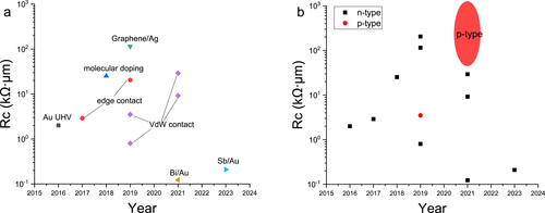
Table 4. Recent progress of TMDCs TFTs.
A complete understanding of the causes and effects of contact resistance is necessary to improve TMDCs Rc. This understanding should be accompanied by research on n-type and p-type devices. Currently, the reason for the higher contact resistance of p-type TMD transistors compared to n-type TMD transistors is unclear, and further research is needed to understand the underlying cause. Furthermore, methods for creating large-area 2D materials for backplane TFTs in the display should be proposed. Most of the research on TMDCs is based on mechanical exfoliation, which is impractical for applications. Therefore, wafer-scale growth methods and solution-based exfoliation and film fabrication methods should be pursued together for large-area electronic applications.
5. Conclusions and perspectives
This paper comprehensively reviews recent progress and current research on TFTs based on metal oxides, metal–halide perovskites, and 2D TMDCs. While LTPS has been widely used in the industry, its high-production cost, limited compatibility with next-generation flexible displays, and high-temperature process have motivated the search for new materials. Materials with high flexibility, low-process temperature, and large-scale production and patterning capability are essential in applying flexible plastic substrates. Thus, the emerging materials should possess excellent material properties and be evaluated based on their fabrication to guide future research on TFTs for display.
Acknowledgments
Gwon Byeon, Seong Cheol Jang, and Taewan Roh contributed equally to this work. This study was supported by the Ministry of Science and ICT through the National Research Foundation, funded by the Korean Government (NRF-2021R1A2C3005401).
Disclosure statement
No potential conflict of interest was reported by the author(s).
Additional information
Funding
Notes on contributors

Gwon Byeon
Gwon Byeon received his B.S. degree in Chemical Engineering from the Pohang University of Science and Technology (POSTECH), Korea, in 2021. He is currently a Ph.D. student in the Department of Chemical Engineering at POSTECH under the supervision of Prof. Yong-Young Noh. His research interests include solution-processed 2D semiconducting materials for thin-film transistors.
Seong Cheol Jang
Seong Cheol Jang received his B.S. and M.S. degrees (2021) at the Department of Material Science and Engineering of Chungnam National University (CNU), Republic of Korea. He is currently working toward A doctoral degree at CNU. He has been researching oxide/nitride semiconductors, thin-film transistors (TFTs), polymer gate dielectrics, and flexible/stretchable devices.

Taewan Roh
Taewan Roh received his B.S. degree in Chemical Engineering from the Pohang University of Science and Technology (POSTECH) in 2021. He is currently a Ph.D. candidate in the Department of Chemical Engineering at POSTECH under the supervision of Prof. Yong-Young Noh. His research interests include the development of perovskite-based semiconductors through solution-process and thermal deposition, as well as their applications in transistors and circuits.

Ji-Min Park
Ji-Min Park is currently a Ph.D. student in the Department of Materials Science and Engineering in Chungnam National University (CNU), supervised by Prof. Hyun-Suk Kim. Her research interests include oxide/nitride semiconductors, bipolar semiconductors, thin-film transistors (TFTs), and neuromorphic devices.

Hyun-Suk Kim
Hyun-Suk Kim received his Ph.D. from the Korea Advanced Institute of Science and Technology (KAIST), Korea, in 2006. After completing a postdoctoral fellowship at MIT, USA from 2007 to 2009, he joined the Samsung Advanced Institute of Technology as a research staff member of the Display Devices Lab. In 2014, he moved to Chungnam National University, Republic of Korea as assistant professor. He is currently a professor in the Department of Materials Science and Engineering, Chungnam National University. His current research interests are thin film transistor, MOSFET, CMOS devices, all-solid-state-battery, materials design & modeling, thin film coating technologies, and surface & interface analyses.

Yong-Young Noh
Yong-Young Noh is Chair Professor of the Department of Chemical Engineering of Pohang University of Science and Technology (POSTECH). He received his Ph.D. degree in 2005 from GIST and then worked as a postdoctoral associate at the Cavendish Laboratory in Cambridge, UK. Afterward, he worked as a senior researcher at ETRI, as assistant professor at Hanbat National University, and as an associate professor at Dongguk University. His research interest is in developing printable semiconductors, including 2D materials, organic, carbon nanotubes, perovskite, metal halide, and metal oxide for field-effect transistors, photodetectors, and light-emitting diodes.
References
- M.K. Choi, J. Yang, T. Hyeon, and D.-H. Kim, npj Flexible Electron 2, 10 (2018).
- H.J. Jang, J.Y. Lee, J. Kwak, D. Lee, J.-H. Park, B. Lee, and Y.Y. Noh, J Inf. Disp 20, 1–8 (2019).
- H. Zhu, E.-S. Shin, A. Liu, D. Ji, Y. Xu, and Y.-Y. Noh, Adv. Funct. Mater 30, 1904588 (2020).
- M. Chhowalla, D. Jena, and H. Zhang, Nat. Rev. Mater. 1, 16052 (2016).
- M.H. Cho, C.H. Choi, H.J. Seul, H.C. Cho, and J.K. Jeong, ACS Appl. Mater. Interfaces 13, 16628 (2021).
- J. Sheng, T. Hong, H.-M. Lee, K. Kim, M. Sasase, J. Kim, H. Hosono, and J.-S. Park, ACS Appl. Mater. Interfaces 11, 40300 (2019).
- M.H. Cho, M.J. Kim, H. Seul, P.S. Yun, J.U. Bae, K.-S. Park, and J.K. Jeong, J. Inf. Displ. 20, 73 (2019).
- H.J. Yang, H.J. Seul, M.J. Kim, Y. Kim, H.C. Cho, M.H. Cho, Y.H. Song, H. Yang, and J.K. Jeong, ACS Appl. Mater. Interfaces 12, 52937 (2020).
- H. Klasens, and H. Koelmans, Solid State Electronics 7, 701 (1964).
- K. Nomura, H. Ohta, A. Takagi, T. Kamiya, M. Hirano, and H. Hosono, Nature 432, 488 (2004).
- H.J. Seul, M.J. Kim, H.J. Yang, M.H. Cho, M.H. Cho, W.-B. Song, and J.K. Jeong, ACS Appl. Mater. Interfaces 12, 33887 (2020).
- Y. Shin, S.T. Kim, K. Kim, M.Y. Kim, S. Oh, and J.K. Jeong, Sci. Rep. 7, 1 (2017).
- M. Furuta, K. Shimpo, T. Kataoka, D. Tanaka, T. Matsumura, Y. Magari, R. Velichko, D. Sasaki, E. Kawashima, and Y. Tsuruma, presented at SID Symposium Digest of Technical Papers 2021.
- Y. Magari, T. Kataoka, W. Yeh, and M. Furuta, Nat. Commun. 13, 1078 (2022).
- H.J. Park, T. Kim, M.J. Kim, H. Lee, J.H. Lim, and J.K. Jeong, Ceram. Int. 48, 12806 (2022).
- B.K. Kim, N. On, C.H. Choi, M.J. Kim, S. Kang, J.H. Lim, and J.K. Jeong, IEEE Electron Device Lett. 42, 347 (2021).
- K.T. Kim, J. Kim, Y.-H. Kim, and S.K. Park, IEEE Electron Device Lett. 35, 850 (2014).
- J.Y. Choi, S. Kim, D.H. Kim, and S.Y. Lee, Thin Solid Films 594, 293 (2015).
- B.H. Lee, A. Sohn, S. Kim, and S.Y. Lee, Sci. Rep. 9, 1 (2019).
- H. Ji, A.Y. Hwang, C.K. Lee, P.S. Yun, J.U. Bae, K.-S. Park, and J.K. Jeong, IEEE Trans. Electron Devices 62, 1195 (2015).
- T. Kim, M.J. Kim, J. Lee, and J.K. Jeong, ACS Appl. Mater. Interfaces 11, 22501 (2019).
- S.T. Kim, Y. Shin, P.S. Yun, J.U. Bae, I.J. Chung, and J.K. Jeong, Electron. Mater. Lett. 13, 406 (2017).
- H.W. Zan, C.C. Yeh, H.F. Meng, C.C. Tsai, and L.H. Chen, Adv. Mater. 24, 3509 (2012).
- J.-M. Park, H.-D. Kim, H. Joh, S.C. Jang, K. Park, Y.C. Park, H.-H. Nahm, Y.-H. Kim, S. Jeon, and H.-S. Kim, NPG Asia Mater. 12, 1 (2020).
- T.J. Yen, A. Chin, and V. Gritsenko, Nanomaterials 11, 92 (2021).
- H.-M. Kim, S.-H. Choi, H.J. Jeong, J.-H. Lee, J. Kim, and J.-S. Park, ACS Appl. Mater. Interfaces 13, 30818 (2021).
- J.H. Bae, J.H. Lee, S.P. Park, T.S. Jung, H.J. Kim, D. Kim, S.-W. Lee, K.-S. Park, S. Yoon, and I. Kang, ACS Appl. Mater. Interfaces 12, 38350 (2020).
- W. Maeng, S.-H. Lee, J.-D. Kwon, J. Park, and J.-S. Park, Ceram. Int. 42, 5517 (2016).
- F. Shan, A. Liu, H. Zhu, W. Kong, J. Liu, B. Shin, E. Fortunato, R. Martins, and G. Liu, J. Mater. Chem. C 4, 9438 (2016).
- J. Yang, B. Wang, Y. Zhang, X. Ding, and J. Zhang, J. Mater. Chem. C 6, 12584 (2018).
- A. Liu, H. Zhu, Z. Guo, Y. Meng, G. Liu, E. Fortunato, R. Martins, and F. Shan, Adv. Mater. 29, 1701599 (2017).
- A. Zavabeti, P. Aukarasereenont, H. Tuohey, N. Syed, A. Jannat, A. Elbourne, K.A. Messalea, B.Y. Zhang, B.J. Murdoch, and J.G. Partridge, Nat. Electron. 4, 277 (2021).
- C. Zhao, C. Tan, D.-H. Lien, X. Song, M. Amani, M. Hettick, H.Y.Y. Nyein, Z. Yuan, L. Li, and M.C. Scott, Nat. Nanotechnol. 15, 53 (2020).
- T. Kim, C.H. Choi, P. Byeon, M. Lee, A. Song, K.-B. Chung, S. Han, S.-Y. Chung, K.-S. Park, and J.K. Jeong, npj 2D Mater. Appl. 6, 4 (2022).
- a) J.S. Park, K.S. Son, T.S. Kim, J.S. Jung, K.-H. Lee, W.-J. Maeng, H.-S. Kim, E.S. Kim, K.-B. Park, and J.-B. Seon, IEEE Electron Device Letters 2010, 31, 960; b) K.-S. Son, J.-S. Jung, K.-H. Lee, T.-S. Kim, J.-S. Park, Y.-H. Choi, K. Park, J.-Y. Kwon, B. Koo, S.-Y. Lee, IEEE electron device letters 2010, 31, 219.
- S. Hu, K. Lu, H. Ning, Z. Zheng, H. Zhang, Z. Fang, R. Yao, M. Xu, L. Wang, and L. Lan, IEEE Electron Device Lett. 38, 879 (2017).
- Y. Shin, S.T. Kim, K. Kim, M.Y. Kim, S. Oh, and J.K. Jeong, Sci. Rep. 7, 10885 (2017).
- J.-M. Park, H. Lee, G. Lee, S.C. Jang, Y.H. Chang, H. Hong, K.-B. Chung, K.J. Lee, D.H. Kim, and H.-S. Kim, ACS App. Mater. Interfaces 15, 1525 (2022).
- a) S. Bai, P. Da, C. Li, Z. Wang, Z. Yuan, F. Fu, M. Kawecki, X. Liu, N. Sakai, J.T. Wang, S. Huettner, S. Buecheler, M. Fahlman, F. Gao, and H.J. Snaith, Nature, 571, 245 (2019); b) X.-K. Liu, W. Xu, S. Bai, Y. Jin, J. Wang, R. H. Friend, F. Gao, Nature Materials 2021, 20, 10; c) J. Y. Kim, J. W. Lee, H. S. Jung, H. Shin, N. G. Park, Chem Rev 2020, 120, 7867; d) Q. Jiang, M. Chen, J. Li, M. Wang, X. Zeng, T. Besara, J. Lu, Y. Xin, X. Shan, B. Pan, C. Wang, S. Lin, T. Siegrist, Q. Xiao, Z. Yu, ACS Nano 2017, 11, 1073.
- D.B.M.C.R. Kagan, and C.D. Dimitrakopoulos, Science 286, 945 (1999).
- K. Zheng, and T. Pullerits, The J. Phys. Chem. Lett. 10, 5881 (2019).
- a) F. Zhang, D.H. Kim, H. Lu, J.-S. Park, B.W. Larson, J. Hu, L. Gao, C. Xiao, O.G. Reid, X. Chen, Q. Zhao, P.F. Ndione, J.J. Berry, W. You, A. Walsh, M.C. Beard, and K. Zhu, J. Am. Chem. Soc., 141, 5972 (2019); b) F. Zhang, D. H. Kim, K. Zhu, Current Opinion in Electrochemistry 2018, 11, 105.
- a); b) S. Zhou, G. Zhou, Y. Li, X. Xu, Y.-J. Hsu, J. Xu, N. Zhao, and X. Lu, ACS Energy Lett., 5, 2614 (2020).
- B. Jeong, L. Veith, T. Smolders, M.J. Wolf, and K. Asadi, Adv Mater 33, e2100486 (2021).
- W. Ke, and M.G. Kanatzidis, Nat. Commun. 10, 965 (2019).
- H. Zhu, A. Liu, K.I. Shim, H. Jung, T. Zou, Y. Reo, H. Kim, J.W. Han, Y. Chen, H.Y. Chu, J.H. Lim, H.J. Kim, S. Bai, and Y.Y. Noh, Nat Commun 13, 1741 (2022).
- D. Meggiolaro, D. Ricciarelli, A.A. Alasmari, F.A.S. Alasmary, and F. De Angelis, The J. Phys. Chem. Lett. 11, 3546 (2020).
- G. Abiram, F.H. Gourji, S. Pitchaiya, P. Ravirajan, T. Murugathas, and D. Velauthapillai, Sci Rep 12, 2455 (2022).
- T. Matsushima, S. Hwang, A.S. Sandanayaka, C. Qin, S. Terakawa, T. Fujihara, M. Yahiro, and C. Adachi, Adv Mater 28, 10275 (2016).
- Y. Li, K. Cui, X. Xu, J. Chen, Y. Liu, J. Wu, S. Lu, W. Qin, and X. Wu, The J. Phys. Chem. C 124, 15107 (2020).
- X. Hu, H. Zhou, Z. Jiang, X. Wang, S. Yuan, J. Lan, Y. Fu, X. Zhang, W. Zheng, X. Wang, X. Zhu, L. Liao, G. Xu, S. Jin, and A. Pan, ACS Nano 11, 9869 (2017).
- L. Tang, Y. Peng, Z. Zhou, Y. Wu, J. Xu, J. Li, Y. Du, L. Huang, H. Cai, J. Ni, and J. Zhang, Appl. Phy. A 124, 624 (2018).
- W. Yu, F. Li, L. Yu, M.R. Niazi, Y. Zou, D. Corzo, A. Basu, C. Ma, S. Dey, M.L. Tietze, U. Buttner, X. Wang, Z. Wang, M.N. Hedhili, C. Guo, T. Wu, and A. Amassian, Nat. Commun 9, 5354 (2018).
- J. Wang, S.P. Senanayak, J. Liu, Y. Hu, Y. Shi, Z. Li, C. Zhang, B. Yang, L. Jiang, D. Di, A.V. Ievlev, O.S. Ovchinnikova, T. Ding, H. Deng, L. Tang, Y. Guo, J. Wang, K. Xiao, D. Venkateshvaran, L. Jiang, D. Zhu, and H. Sirringhaus, Adv. Mater 31, e1902618 (2019).
- T. Matsushima, M.R. Leyden, T. Fujihara, C. Qin, A.S.D. Sandanayaka, and C. Adachi, Appl. Phys. Lett., 115 (2019).
- H. Shen, J. Li, H. Wang, J. Ma, J. Wang, H. Luo, and D. Li, J Phys Chem Lett 10, 7 (2019).
- Y. Meng, C. Lan, F. Li, S. Yip, R. Wei, X. Kang, X. Bu, R. Dong, H. Zhang, and J.C. Ho, ACS Nano 13, 6060 (2019).
- J. Li, Z. Zhou, Y. Peng, J. Zhang, N. Guo, and Y. Sun, Org. Electron., 84 (2020).
- A.N. Aleshin, I.P. Shcherbakov, O.P. Chikalova-Luzina, L.B. Matyushkin, M.K. Ovezov, A.M. Ershova, I.N. Trapeznikova, and V.N. Petrov, Synth. Metals 260 (2020).
- H. Zhu, A. Liu, K.I. Shim, J. Hong, J.W. Han, and Y.Y. Noh, Adv Mater 32, e2002717 (2020).
- S.P. Senanayak, M. Abdi-Jalebi, V.S. Kamboj, R. Carey, R. Shivanna, T. Tian, G. Schweicher, J. Wang, N. Giesbrecht, D. Di Nuzzo, H.E. Beere, P. Docampo, D.A. Ritchie, D. Fairen-Jimenez, R.H. Friend, and H. Sirringhaus, Sci Adv 6, eaaz4948 (2020).
- N. Guo, J. Li, S. Yang, J. Zhang, J. Ni, and H. Cai, Nanotechnology 32 (2021).
- S. Shao, W. Talsma, M. Pitaro, J. Dong, S. Kahmann, A.J. Rommens, G. Portale, and M.A. Loi, Adv. Funct. Mater. 31, 2008478 (2021).
- A. Liu, H. Zhu, S. Bai, Y. Reo, T. Zou, M.-G. Kim, and Y.-Y. Noh, Nature Electron. 5, 78 (2022).
- Y. Liu, P.A. Chen, X. Qiu, J. Guo, J. Xia, H. Wei, H. Xie, S. Hou, M. He, X. Wang, Z. Zeng, L. Jiang, L. Liao, and Y. Hu, iScience 25, 104109 (2022).
- ACS Nano 2013, 7, 4, 2898–2926, 2013, progress, challenges, and opportunities in Two-Dimensional Materials Beyond Graphene.
- Nature Nanotechnology 7, 699-712 (2012), Electronics and optoelectronics of two-dimensional transition metal dichalcogenides.
- Nature Reviews Materials 1, 16052 (2016),: Two-dimensional semiconductors for transistor.
- K. Cho, J. Park, J. Kim, K. Kang, T. Kim, J. Shin, B. Choi, S. Chung, and T. Lee, Adv. Mater 30, 1705540 (2018).
- Y. Du, H. Liu, A.T. Neal, M. Si, and P.D. Ye, IEEE Electron Device Lett 34, 1328–1330 (2013).
- R. Kappera, D. Voiry, S.E. Yalcin, B. Branch, G. Gupta, A.D. Mohite, and M. Chhowalla, Nat. Mater 13, 1128–1134 (2014).
- S.-S. Chee, D. Seo, H. Kim, H. Jang, S. Lee, S. Moon, K. Lee, S. Kim, H. Choi, and M. Ham, Adv. Mater 31, 1804422 (2019).
- Y. Liu, J. Guo, Y. Wu, E. Zhu, N.O. Weiss, Q. He, H. Wu, H.-C. Cheng, Y. Xu, I. Shakir, Y. Huang, and X. Duan, Nano Lett 16, 6337–6342 (2016).
- K.K.H. Smithe, S.V. Suryavanshi, M. Munoz Rojo, A.D. Tedjarati, and E. Pop, ACS Nano 11, 8456 (2017).
- Z. Cheng, Y. Yu, S. Singh, K. Price, S.G. Noyce, Y. Lin, L. Cao, and A.D. Franklin, Nano Lett 19, 5077 (2019).
- Y. Jung, M. Choi, A. Nipane, A. Borah, B. Kim, A. Zangiabadi, T. Taniguchi, K. Watanabe, W. Yoo, J. Hone, and J.T. Teherani, Nature Electronics 2, 187 (2019).
- Y. Wang, et al., Van der Waals contacts between three-dimensional metals and two-dimensional semiconductors, Nature 568, 70–74 (2019).
- P.C. Shen, et al., Ultralow contact resistance between semimetal and monolayer semiconductors, Nature 593, 211–217 (2021).
- W. Li, X. Gong, Z. Yu, L. Ma, W. Sun, S. Gao, J. Wang, and X. Wang, Nature 613, 274 (2023).
- Y. Liu, J. Guo, and E. Zhu, Nature 557, 696 (2018).
- S.G. Louie, and M.L. Cohen, Electronic structure of a metal-semiconductor interface, Phys. Rev. B 13, 2461–2469 (1976).
- T. Nishimura, K. Kita, and A. Toriumi, Evidence for strong Fermi-level pinning due to metal-induced gap states at metal/germanium interface, Appl. Phys. Lett 91, 123123 (2007).
- M. Kobayashi, A. Kinoshita, K. Saraswat, H.-S.P. Wong, and Y. Nishi, Fermi level depinning in metal/Ge Schottky junction for metal source/drain Ge metal-oxide-semiconductor field-effect-transistor application, J. Appl. Phys 105, 023702 (2009).
- K. Sotthewes, et al., Universal Fermi-level pinning in transition-metal dichalcogenides, J. Phys. Chem. C 123, 5411–5420 (2019).
- C.D. English, G. Shine, V.E. Dorgan, K.C. Saraswat, and E. Pop, Nano Lett 16, 3824 (2016).
- A. Sebastian, R. Pendurthi, T.H. Choudhury, J.M. Redwing, and S. Das, Benchmarking monolayer MoS2 and WS2 field-effect transistors, Nat. Commun 12, 693 (2021).
- C. Kim, et al., Fermi level pinning at electrical metal contacts of monolayer molybdenum dichalcogenides, ACS Nano 11, 1588–1596 (2017).
- N. Kaushik, et al., Schottky barrier heights for Au and Pd contacts to MoS2, Appl. Phys. Lett 105, 113505 (2014).