
 ?Mathematical formulae have been encoded as MathML and are displayed in this HTML version using MathJax in order to improve their display. Uncheck the box to turn MathJax off. This feature requires Javascript. Click on a formula to zoom.
Abstract
Efficient charge generation is essential for tandem organic light-emitting diode (OLED) devices. In this study, we introduce a p-type copper iodide (CuI) layer within the charge generation layer (CGL) that exhibits high charge generation efficiency in tandem OLED devices. Briefly, CuI is deposited as a thin layer via thermal evaporation technique. X-ray diffraction (XRD) analysis reveals the formation of γ-CuI, and the ultraviolet-visible (UV-Vis) spectral analysis demonstrates outstanding optical transparency (∼95%) of the deposited CuI films in the visible range. The current-voltage (I-V) and capacitance-voltage (C-V) analyses show that the p-type CuI layer is a vital and excellent charge generator and enhances the current density significantly. The tandem OLED device fabricated using Bphen:Liq/CuI/HAT-CN as the CGL results in a substantial 1.9-fold increase in current efficiency compared to the single-unit OLED device, approaching the theoretical two-fold increase. These findings highlight the potential of CuI as a promising p-type material for CGL design in tandem OLED devices.
1. Introduction
Since the pioneering study by C.W. Tang and Van Slyke in 1987, organic light-emitting diodes (OLEDs) have made significant strides and emerged as a crucial technology in the display industry [Citation1,Citation2]. Thanks to their thin form factor and outstanding image quality performance, OLEDs offer enormous potential for advanced display applications [Citation3,Citation4]. However, maintaining high luminance over a prolonged period remains a significant challenge for OLEDs. Substantial advancements in OLED technology have led to the development of tandem OLEDs to address this issue, especially in large-size displays [Citation5]. Tandem OLEDs use stacked two or more light-emitting units, which increases the driving voltage compared to a single-unit OLED but offers greater current efficiency proportional to the number of stacked units. Consequently, the current required to produce the desired luminance is significantly reduced, increasing the lifespan of the device.
Tandem OLEDs require a charge generation layer (CGL) between two stacked electroluminescence (EL) units. An ideal CGL should exhibit efficient charge generation, high optical transparency, and a low energy barrier for charge injection to adjacent layers. Therefore, significant research and development efforts are underway to improve the performance of CGLs [Citation6–12]. CGLs are typically constructed using n–p junctions in three different types: (i) an n-doped organic layer/p-type transition metal oxide layer [Citation13–16], (ii) an n-doped organic layer/p-doped organic layer [Citation17,Citation18], and (iii) a non-doped n–p organic heterojunction [Citation19–21]. Among these types, the first type is the most popular, wherein typical transition metal oxides such as TiO2, WO3, and MoO3 serve as the p-type layer. Inorganic p-type materials provide several advantages over p-doped organic materials, such as easy synthesis, low cost, and high optical transparency in the visible range. However, the high melting points of metal oxides can make the thermal evaporation process difficult [Citation22]. Thus, an alternative inorganic p-type material for a CGL is required to mitigate the above issue.
Recently, there has been a growing interest in γ-copper iodide (γ-CuI), a typical metal halide semiconductor with a bandgap of 3.1 eV, for its use as a p-type material [Citation23]. γ-CuI exhibits significantly high hole mobility and conductivity due to two main factors. First, the valence band maximum of γ-CuI has a more dispersed hole distribution, attributed to iodine's lower electronegativity than oxygen. Second, a copper vacancy in γ-CuI creates an acceptor energy state above the valence band maximum. In addition, γ-CuI boasts excellent transparency, reaching over 80% even at a film thickness of 100 nm [Citation24]. Its relatively low melting point and low cost render it an energy-efficient and cost-effective p-type material [Citation25–27]. Consequently, CuI is often utilized as a hole injection or transport layer in OLEDs [Citation28,Citation29], solar cells [Citation30–32], and as a transparent electrode in flexible electronics [Citation23]. However, to the best of our knowledge, there have been no reports on the use of CuI for a CGL in tandem OLED devices.
This study reported CuI-based CGL, constructed in the following structure: n-Bphen:Liq/p-CuI/HAT-CN for its use in a tandem OLED device. The physical properties of the CuI film and the effect of CuI on charge generation device performance are systematically investigated. The optoelectronic performance of the tandem device fabricated with the CuI-based CGL is examined and compared with that of the single OLED device. The results show that CuI is a promising p-type material for CGL for optoelectronic devices, including tandem OLEDs.
2. Experiment
All devices were fabricated on glass substrates, with a patterned indium-tin-oxide (ITO) serving as an anode. To define the light-emitting area, a pixel-define-layer (PDL) with the dimensions of 2 mm × 2 mm and a thickness of 5 µm was deposited on the ITO substrates. The substrates were then cleaned with ethanol and deionized water using ultrasonication, followed by gentle heating to remove any remaining solvent. Subsequently, O2 plasma treatment was performed under high-vacuum conditions of 5.0 × 10⁻⁶ Torr. The evaporation of organic and inorganic materials for the device fabrication was performed using an evaporation equipment system (SUNICEL Plus 200) in separate organic and metal chambers, respectively, under the same high-vacuum condition.
Then, the following materials were deposited in an organic chamber: 1,4,5,8,9,11-Hexaazatriphenylene hexacarbonitrile (HAT-CN) as the hole injection layer (HIL), N, N'-bis(1-naphthyl)-N, N'-diphenyl-(1,1'-biphenyl)−4,4'-diamine (NPB) as the hole transport layer (HTL), 4,4'-Bis(9-carbazolyl)−1,1'-biphenyl (CBP) as the host material of the emission layer (EML), and Tris[2-phenylpyridine]iridium(III) (Ir(ppy)3) as the dopant. The doping ratio of the host and dopant materials was maintained at 10:1, respectively. Additionally, 2,2’,2"-(1,3,5-Benzinetriyl)-tris(1-phenyl-1-H-benzimidazole) (TPBi) was employed as the hole blocking and electron transport layer (ETL), and bathophenanthroline (Bphen) was used as an additional ETL. Furthermore, the n-type electron injection layer (EIL) was prepared by doping Bphen with Lithium-8-hydroxyquinolinolate (Liq) at a ratio of 1:1 [Citation33]. Copper iodide (CuI) served as a p-type material for CGL and was deposited in a metal chamber (MC). Finally, aluminum (Al) was also deposited in the MC as the cathode. All devices were encapsulated under a nitrogen (N2) atmosphere. The structures of the single-unit and tandem OLED devices are depicted in Figure .
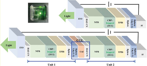
Figure 1. The structures of single-unit (top) and tandem (bottom) devices. The inset photo is the fabricated tandem OLED.
The transmittance of the CuI film was determined by using UV–Vis (UV-2600) equipment. X-ray diffraction (XRD) measurements were performed using Bruker D8 ADVANCE equipment. Ultraviolet photoelectron spectroscopy (UPS) measurement was performed using (ESCALAB250) to measure the energy levels of the samples. The capacitance-voltage (C-V) measurement was performed using the Solartron 1296 Dielectric interface and the SI 1260 Impedance / Gain phase analyzer. The current, voltage, and luminance characteristics of all devices were measured using an I-V-L measurement system composed of a Keithley-2400 source meter and a CS-2000 spectroradiometer in a dark box.
3. Results and discussion
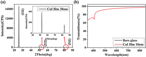
As represented in Figure , the tandem OLED device is composed of two sets of single-unit devices, and the γ-CuI layer is additionally inserted between the two units. In general, CuI exists in three crystal structures, while rock salt structure (α-CuI) and wurtzite structure (β-CuI) are conductors, zinc blende γ-CuI structure is a p-type semiconductor. γ-CuI can be deposited at a relatively low temperature of 643 K, which is an advantage for OLED devices. It also has a high hole mobility of 43.9 cm2V−1S−1, which is higher than typical oxide-based p-type semiconductors [Citation34–36]. In this study, a CuI thin layer was thermally deposited on a glass substrate by using CuI powder in a vacuum evaporation chamber. The XRD patterns of the deposited films, as shown in Figure (a), revealed three peaks located at 2Θ = 25.52°, 52.3°, and 82.8°, with the major peak at 25.52°. These patterns correspond to the (111), (222), and (511) planes of the zinc blende crystal structure (PDF 00-006-0246) of γ-CuI [Citation25–27], confirming the successful deposition of CuI films with a preferred orientation along the (111) direction. Figure (b) illustrates the transmission spectrum of the deposited CuI film in the spectral range of 300 nm–900 nm. The spectrum demonstrated that the CuI film exhibited an average transmittance of 94.6% in the range of 410 nm–800 nm, indicating outstanding transparency in the visible range.
Figure 2. (a) XRD patterns and (b) UV–Vis transmittance spectra of thermally evaporated CuI film deposited on a glass substrate.
The ratio of 1:1 was chosen for the Bphen:Liq mixture as it has been reported to exhibit good electrical properties in the literature [Citation33]. However, there has been no clear report on the energy levels of Bphen:Liq at this mixing ratio; hence, these were determined experimentally to construct the band diagram of the fabricated tandem device.
The highest occupied molecular orbital (HOMO) and the lowest unoccupied molecular orbital (LUMO) energy of Bphen:Liq were determined using UPS (Figure (a)) and Tauc plot (Figure (b)) derived from the UV–Vis spectrum. Briefly, the HOMO (i.e. the ionization potential) is defined by the following equation: [Citation37]
(1)
(1) where
is the source energy,
is a secondary cut-off point, and
is the distance from the Fermi edge to the HOMO level. The
and
for Bphen:Liq were determined as 16.9 and 3.4 eV, respectively, from the UPS spectra, as reflected in Figure (b). The
is an experimental parameter, which is 21.01 eV for He1. According to equation (1), the HOMO of Bphen:Liq was calculated as 7.5 eV.
Figure 3. (a) UPS graph and (b) Tauc plot of Bphen:Liq, (c) schematic band diagram of the tandem device.

The energy gap between the HOMO and LUMO of Bphen:Liq was determined from the UV-Vis spectrum (Figure (c)) and by applying a Tauc plot, as shown below:
(2)
(2) where α is the absorption coefficient, h is the Planck constant, ν is the photon’s frequency, Eg is the bandgap energy, A is a constant, and n has the value of 1/2 for a direct energy gap material like Bphen:Liq [Citation38]. The extrapolation of the linear portion of the Tauc plot yielded a bandgap of 4.1 eV for Bphen:Liq. Subtracting this value from the HOMO energy level provides the LUMO energy level of 3.4 eV.
The energy levels of bulk γ-CuI and all other materials were well demonstrated earlier, and their corresponding energy values were obtained from the literature [Citation8]. With the above values, the band diagram of the tandem device was constructed. Figure (c) exhibits that the HOMO level of Bphen becomes deeper after doping with Liq. In addition, the energy difference between the LUMO of Bphen:Liq and the conduction band of CuI is 1.7 eV, which is 0.3 eV narrower than that of Bphen:Liq and HAT-CN.
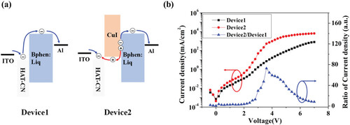
To verify the charge generation ability of CuI, two devices were fabricated with and without the CuI layer, labeled as Device 1 and Device 2, respectively, as displayed in Figure (a). Device 2 has the same layer structure as the CGL in the tandem device, except that it has an inverted layer order, which was chosen to better match with the energy levels of the anode and cathode electrodes. The performance of the devices is depicted in Figure (b), where the current density of Device 2 with CuI at 3.6 V is 525 mA/cm2, which is ∼72 times higher than the current density of Device 1 without CuI. This large difference is explained as follows: In Device 1, an electron-only device, the Bphen:Liq layer simply acts as an electron transfer channel, wherein the Bphen:Liq and HAT-CN interface hinders the charge flow, reducing the current density. When a p-type CuI layer is inserted as in Device 2, high concentrations of free holes and electrons are generated at the interface of Bphen:Liq and CuI. Moreover, the HOMO level of CuI is matched with the LUMO of HATCN, and the separated electrons from the interface are transported through the LUMO of HATCN, which has high electron mobility [Citation39]. Consequently, the current density in Device 2 is significantly higher than that of Device 1, indicating the capability of CuI in terms of efficient charge generation.
Figure 4. (a) Band diagram of devices prepared with and without CuI, (b) corresponding plot of current density versus voltage and comparison of I–V performance between Device 2 and Device 1.
We analyzed the capacitance-voltage (C-V) characteristics to investigate the field-assisted charge generation process of CGL. For this purpose, CGL devices with double insulation layers were fabricated, as illustrated in Figure (a), where 30 nm thick LiF layers were inserted between the external electrodes and the CGL. The LiF insulation layers block charge injection from the external electrodes, enabling observation of the internal charge flow within the CGL. The capacitance of the devices was measured at varying direct current (DC) voltages from −8 V to +8 V with 100 Hz and 0.5 mV alternating current signal, as indicated in Figure (b).
Figure 5. (a) Band diagram of CGL devices with double insulation layers prepared with and without CuI (Devices 3 and 4, respectively). (b) Capacitance versus voltage (C-V) plots of Device 3 and Device 4.
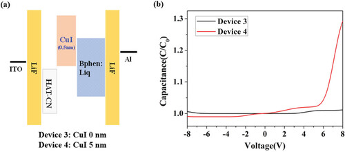
In the case of Device 3 without CuI, the capacitance remains almost unchanged with varying applied DC voltage, indicating no charge generation. In contrast, Device 4 with a 5 nm CuI layer exhibits a sharp increase of capacitance starting from around 6 V, reaching up to 1.3 times higher than that at zero bias. The sharp increase in capacitance suggests that internal charges can move under the bias DC voltage, demonstrating the occurrence of charge generation [Citation39–41].
The light-emitting and current-voltage characteristics of both single device and tandem device with CuI CGL are exemplified in Figure . The electroluminescence (EL) spectra (Figure (a)) of the single and tandem devices exhibit emission at the same wavelength, suggesting that adding an extra unit for the tandem structure does not affect the emission properties. However, a slight reduction (∼10 nm) in the full width at half maximum (FWHM) of the spectrum was observed. This narrowing of the spectrum may be attributed to a microcavity effect. Nevertheless, since this microcavity effect is weak, it is deemed to have minimal impact on the operation of the tandem device, and its effects can be disregarded [Citation17,Citation42].
Figure 6. (a) Normalized EL spectrum of single and tandem devices, (b) Current density versus applied voltage (c) Luminance versus current density, (d) Current efficiency (left side) and EQE (right side) versus current density of single unit and tandem devices.
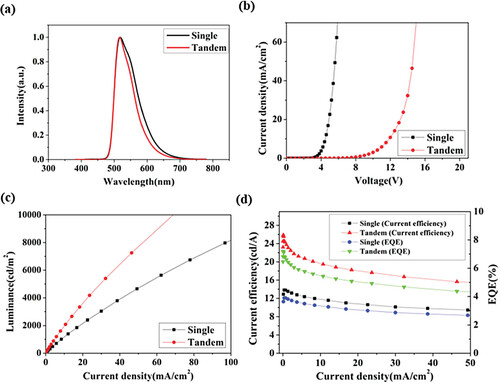
Figure (b) depicts the plot of current density versus voltage for both single and tandem devices. Upon considering the point of 0.1 mA/cm2 as the turn-on voltage, it is observed that the turn-on voltage for a single unit device is 2.9 V, while for a CuI-inserted tandem device, it is 6.6 V, which is slightly higher than twice (5.8 V) of that for a single unit device. As shown in Figure (c), to achieve a luminescence of 1000 cd/m2, the single unit device required a current density of 8.4 mA/cm2, whereas the tandem device required 4.9 mA/cm2, which is only slightly higher than half of the current density (4.2 mA/cm2) of the single unit device. In addition, the maximum current efficiency and external quantum efficiency (EQE) of the tandem device is measured to be 25.8 cd/A (7.2%), which is 1.9 (1.84) times higher than that of the single device with a current efficiency of 13.5 cd/A (3.9%) (Figure (d)). For an ideal tandem device, the turn-on voltage and maximum current efficiency and EQE for a tandem device are expected to be twice of a single unit. However, in real tandem devices, the turn-on voltage may increase more than twice, because the device thickness increases more than twice due to the insertion of additional CGLs, in this case, the CuI layer. Moreover, the current efficiency increase is also usually less than twice due to the internal light loss caused by the stacked emission structures. Therefore, the improvement of 1.9 times in current efficiency in this tandem device can be regarded as an excellent result. Overall, these results suggest that the tandem device constructed with a CuI-based CGL operates quite well.
4. Conclusion
A thin film of metal halide γ-CuI, serving as a p-type material of a CGL, was easily obtained through thermal evaporation. The film exhibited a high optical transparency of approximately 95% in the visible range. The charge generation device was constructed by inserting a p-type CuI layer between the n-type Bphen:Liq EIL and p-type HAT-CN HIL in the stacked single-EL devices. The incorporation of CuI significantly enhanced the current density within the device, confirming improved charge generation with CuI. Tandem OLED was then successfully fabricated with CuI-based CGL, and a current efficiency of 1.9 (1.84) times, close to the theoretical limit of twice the single-unit device, was obtained. Specifically, the current efficiency was 13.5 cd/A (3.9%) for the single-unit device and 25.8 cd/A (7.2%) for the tandem device. Furthermore, at an operating luminance of 1,000 cd/m2, the current density was 8.4 mA/cm2 for the single-unit device and 4.9 mA/cm2 for the tandem device. Thus, a typical metal halide material, CuI, can be a promising p-type material for enhancing charge generation and could be a viable material for tandem OLED applications.
Acknowledgments
This work was supported by the National Research Foundation of Korea (NRF) (NRF-2022R1A4A1028702, NRF-2022M3D1A2083618, and RS-2023-00241971) and the ICT Creative Consilience Program (IITP-2020-0-01821), funded by the Ministry of Science, ICT, and Future Planning.
Disclosure statement
No potential conflict of interest was reported by the author(s).
Additional information
Funding
Notes on contributors
Kanghoon Kim
Kanghoon Kim: Kanghoon Kim received his B.S. and M.S. degrees from Hanyang University and Sungkyunkwan University, South Korea, in 2014 and 2016, respectively. He joined Samsung Display Company in 2016. He is currently studying a Ph.D. course at Sungkyunkwan University through an academic scholarship program provided by Samsung. His research focuses on tandem structure organic light-emitting diodes.

Jae-In Yoo
Jae-In Yoo: Jae-In Yoo received his B.S. degree from Kyunghee University, South Korea, in 2020. He is currently a Ph.D. student at Sungkyunkwan University. His research focuses on color-tunable light-emitting diodes.

Hyo-Bin Kim
Hyo-Bin Kim: Hyo-Bin Kim received his B.S. and M.S. degrees from Sungkyunkwan University, South Korea, in 2020 and 2022, respectively. He is currently a Ph.D. student at Sungkyunkwan University. His research focuses on the green approach to display field and organic light-emitting diodes.

Sung-Cheon Kang
Sung-Cheon Kang: Sung-Cheon Kang received his B.S. degree from Korea Aerospace University, South Korea, in 2021. He is currently a Ph.D. student at Sungkyunkwan University. His research focuses on color-tunable organic light-emitting diodes.
Jincheol Jang
Jincheol Jang: Jincheol Jang received his M.S. degree from Hanyang University, South Korea in 2014. He is currently a Ph.D. student at Sungkyunkwan University. His research focuses on layer-optimizing light-emitting diodes.

Sundararajan Parani
Sundararajan Parani: Dr. Parani earned his Ph.D. from the Department of Inorganic Chemistry at the University of Madras, India in 2015. Following this, he worked as a postdoctoral researcher at the University of Johannesburg, South Africa until 2021. Currently, he serves as a Research Professor in the Department of Electrical and Electronic Engineering at Sungkyunkwan University, Republic of Korea. His research primarily concentrates on cadmium-free quantum dots including perovskite materials for biomedical, display.

Jang-Kun Song
Jang-Kun Song: Jang-Kun Song received his B.S. and M.S. degrees in physics from Korea University, Seoul, South Korea, in 1994 and 1996, respectively. He also received his Ph.D. degree in electronic engineering from the University of Dublin, Dublin, Ireland, in 2008. He worked in the R&D department of Samsung Electronics Company as a principal engineer from 1996 to 2010. At Samsung, he invented the patterned vertical alignment LCD technology. In 2010, he moved to Sungkyunkwan University, South Korea, where he is currently working as a professor in the School of Electronics and Electrical Engineering. He holds about 240 patents worldwide in display and other technologies. He received the King Sejong Patent Award from the Korean Intellectual Office in 2001.
References
- C.W. Tang, and S.A. VanSlyke, Appl. Phys. Lett. 51, 1 (1987).
- A. Sugimoto, H. Ochi, S. Fujimura, A. Yoshida, T. Miyadera, and M. Tsuchida, IEEE J. Sel. Top. Quantum Electron. 10, 107 (2004).
- C. May, presented at 2021 28th International Workshop on Active-Matrix Flatpanel Displays and Devices (AM-FPD), 29 June-2 July 2021, 2021.
- G. Huseynova, J.-H. Lee, Y.H. Kim, and J. Lee, Adv. Opt. Mater. 9, 2002040 (2021).
- L.S. Liao, K.P. Klubek, and C.W. Tang, Appl. Phys. Lett. 84, 167 (2004).
- Y.-H. Deng, Q.-D. Ou, Q.-K. Wang, H.-X. Wei, Y.-Q. Li, S.-T. Lee, and J.-X. Tang, J. Mater. Chem. C 2, 4 (2014).
- Y.-M. Cheng, H.-H. Lu, T.-H. Jen, and S.-A. Chen, The Journal of Physical Chemistry C 115, 582 (2011).
- P. Xiao, J. Huang, Y. Yu, and B. Liu, Molecules 24, 151 (2019).
- Q. Guo, H. Sun, D. Yang, X. Qiao, J. Chen, T. Ahamad, S.M. Alshehri, and D. Ma, Adv. Mater. Interfaces 3, 1600081 (2016).
- Y. Chen, Q. Wang, J. Chen, D. Ma, D. Yan, and L. Wang, Org. Electron. 13, 1121 (2012).
- K.-H. Han, K. Kim, Y. Han, Y.-D. Kim, H. Lim, D. Huh, H. Shin, H. Lee, and J.-J. Kim, Adv. Mater. Interfaces 7, 1901509 (2020).
- J. Wang, Y. Wang, Y. Qin, R. Li, J.-x. An, Y. Chen, W.-Y. Lai, X. Zhang, and W. Huang, J. Mater. Chem. C 9, 8570 (2021).
- K. Hong, and J.-L. Lee, J. Phys. Chem. C 116, 6427 (2012).
- L. Li, M. Guan, G. Cao, Y. Li, and Y. Zeng, Solid State Commun. 150, 1683 (2010).
- X. Qi, N. Li, and S.R. Forrest, J. Appl. Phys. 107, 014514 (2010).
- H. Yang, J. Kim, K. Yamamoto, and H. Hosono, Org. Electron. 46, 133 (2017).
- W.-h. Park, D.-p. Park, and S.S. Kim, J. Inf. Disp. 23, 45 (2022).
- Y. Xu, Y. Niu, C. Gong, W. Shi, X. Yang, B. Wei, and W.-Y. Wong, Adv. Opt. Mater. 10, 2200984 (2022).
- Q. Chang, Z. Lü, Y. Yin, J. Xiao, and J. Wang, Displays 75, 102306 (2022).
- J. Yuan, W. Liu, J. Yao, Q. Sun, Y. Dai, J. Chen, D. Yang, X. Qiao, and D. Ma, Org. Electron. 83, 105745 (2020).
- H. Sun, Q. Guo, D. Yang, Y. Chen, J. Chen, and D. Ma, ACS Photonics 2, 271 (2015).
- T. Vinod Kumar, and B. Reddy, Catal. Combustion 105 (2011).
- N. Yamada, R. Ino, H. Tomura, Y. Kondo, and Y. Ninomiya, Adv. Electron. Mater. 3, 1700298 (2017).
- P. Storm, M.S. Bar, G. Benndorf, S. Selle, C. Yang, H. von Wenckstern, M. Grundmann, and M. Lorenz, APL Mater. 8, 091115 (2020).
- C. Yang, M. Kneiβ, M. Lorenz, and M. Grundmann, Proc. Natl. Acad. Sci. 113, 12929 (2016).
- D.K. Kaushik, M. Selvaraj, S. Ramu, and A. Subrahmanyam, Sol. Energy Mater. Sol. Cells 165, 52 (2017).
- C. Yang, M. Kneiß, F.-L. Schein, M. Lorenz, and M. Grundmann, Sci. Rep. 6, 21937 (2016).
- P. Stakhira, V. Cherpak, D. Volynyuk, F. Ivastchyshyn, Z. Hotra, V. Tataryn, and G. Luka, Thin Solid Films 518, 7016 (2010).
- M. Shan, H. Jiang, Y. Guan, D. Sun, Y. Wang, J. Hua, and J. Wang, RSC Adv. 7, 13584 (2017).
- W.-Y. Chen, L.-L. Deng, S.-M. Dai, X. Wang, C.-B. Tian, X.-X. Zhan, S.-Y. Xie, R.-B. Huang, and L.-S. Zheng, J. Mater. Chem. A 3, 19353 (2015).
- Y. Peng, N. Yaacobi-Gross, A.K. Perumal, H.A. Faber, G. Vourlias, P.A. Patsalas, D.D.C. Bradley, Z. He, and T.D. Anthopoulos, Appl. Phys. Lett. 106, 243302 (2015).
- S.Z. Haider, H. Anwar, and M. Wang, Semicond. Sci. Technol. 33, 035001 (2018).
- M.S. Ki, M. Sim, O. Kwon, K. Im, B. Choi, B.J. Cha, Y.D. Kim, T.Y. Jin, and K. Paeng, ACS Mater. Lett. 4, 1676 (2022).
- K. Tennakone, G.R.R.A. Kumara, I.R.M. Kottegoda, V.P.S. Perera, G.M.L.P. Aponsu, and K.G.U. Wijayantha, Sol. Energy Mater. Sol. Cells 55, 283 (1998).
- M. Grundmann, F.-L. Schein, M. Lorenz, T. Böntgen, J. Lenzner, and H. von Wenckstern, Phys. Status Solidi A 210, 1671 (2013).
- N. Yamada, R. Ino, and Y. Ninomiya, Chem. Mater. 28, 4971 (2016).
- M. Terashima, T. Miyayama, T. Shirao, H.W. Mo, Y. Hatae, H. Fujimoto, and K. Watanabe, Surf. Interface Anal. 52, 948 (2020).
- P. Makuła, M. Pacia, and W. Macyk, J. Phys. Chem. Lett. 9, 6814 (2018).
- M. Terai, K. Fujita, and T. Tsutsui, Jpn. J. Appl. Phys. 44, L1059 (2005).
- D.-S. Leem, J.-H. Lee, J.-J. Kim, and J.-W. Kang, Appl. Phys. Lett. 93, 103304 (2008).
- S. Lee, J.-H. Lee, J.-H. Lee, and J.-J. Kim, Adv. Funct. Mater. 22, 855 (2012).
- Y. Wen, Y.-K. Wang, J.-G. Zhou, J.-Y. Li, W. He, Y.-J. Zhang, X.-Z. Zhu, L.-S. Liao, and M.-K. Fung, J. Mater. Chem. C 10, 5666 (2022).