
 ?Mathematical formulae have been encoded as MathML and are displayed in this HTML version using MathJax in order to improve their display. Uncheck the box to turn MathJax off. This feature requires Javascript. Click on a formula to zoom.
Abstract
Understanding the deterioration of the charge generation layer (CGL) is an uprising issue for efficient and stable tandem organic light-emitting diodes. Here, we comprehensively investigated the change in the electrical characteristics of Li-doped CGLs according to different stress conditions and compared the stability of Li diffusion in two phenanthroline-based electron transport materials. Through current density–voltage and capacitance-frequency measurements, it was revealed that electrical stress and thermal stress affect CGL’s electrical properties differently. Moreover, the exponential trap distribution model analysis informed that the Li diffusion is expedited toward narrowing depletion width in the CGL. Diffusion of Li and thermal effect to the diffusion was experimentally observed by X-ray photoelectron spectroscopy (XPS) depth profiling. We also evaluated variations in the operating voltage of tandem devices that differed only in nCGL. Overall, Li diffusion occurs more favorably in sparse Bphen film with weak binding energy rather than closely packed BPPB film with strong binding energy, which highlights that atomic geometry and morphological characteristics are crucial for the stability of tandem devices.
Introduction
As augmented reality (AR) and virtual reality (VR) displays requiring high brightness over several thousands of nits and long lifetime are emerging in the future display market, organic light-emitting diodes (OLEDs) have been a promising candidate due to their versatility, high color purity, and mass production [Citation1–3]. In this perspective, a tandem structure with stacked multiple electroluminescence (EL) units is inevitably adopted. Accordingly, there is a growing need to develop an efficient charge generation layer (CGL) that connects each EL unit in serial connection without electrical loss. In general, CGL has a p-n organic heterojunction structure composed of highly conductive p-doped CGL (pCGL) and n-doped CGL (nCGL) for holes and electrons, respectively. As p-dopants, transition metal oxides, such as MoO3[Citation4] and WO3 [Citation5], or deep-lying lowest unoccupied molecular orbital (LUMO) materials, such as F4-TCNQ [Citation6], HAT-CN [Citation6–8], and NDP-9 [Citation9,Citation10] are used. On the other hand, as n-dopants, alkali metals and their composites are mainly used [Citation11–16]. Since organic materials with their weak van der Waals interactions and Coulombic attraction have a sparser packing compared to inorganic materials, the smaller molecules or atoms can diffuse more readily within the organic layers [Citation17] This diffusion can sequentially affect the electrical properties, in addition to undesirable reactions with various molecules in an active device layer. Particularly, even though Li is one of the most used n-dopants for efficient nCGL due to its low work function (2.9 eV), it seems inevitable to prevent its diffusion in the organic layer for its smallest size among alkali metals [Citation18,Citation19]. F.A. Angel et al. reported that Li diffusion into the electron transport layer could affect the electron injection properties and luminance quenching, disrupting the stable performance of tandem devices [Citation20], Yet, in contrast to considerable efforts to examine the degradation factors in single EL unit OLEDs up to this point, the study on CGL deterioration, a pivotal prerequisite for achieving long-lasting tandem OLEDs, remains limited.
This study examined the degradation characteristics of Li-doped nCGLs with two phenanthroline-based – electron transport materials (ETMs) under electrical (J) stress, thermal (T) stress, and electrical and thermal (J – T–) stress simultaneously. It was revealed that electrical stress and thermal stress influence the electrical properties of CGL differently by current – density capacitance – frequency measurements. The Li diffusion proceeds toward narrowing depletion width in the CGL, and this conclusion is confirmed by the exponential trap distribution model analysis. Moreover, the Li diffusion was directly observed via X-ray photon spectroscopy measurement (XPS), and the stability against Li diffusion was further confirmed by comparing the overall characteristics of ETMs, including CGL devices and tandem devices.
Results and discussion
When constructing efficient nCGL, highly reactive alkali metals and compounds with nitrogen-containing heterocycles, such as imidazole, pyridine, and phenanthroline, are typically used. Phenanthroline (Phen) is one of the most prominent candidates featuring rigid heterocyclic planar structure and forming in situ strong coordination with metal or metal ions to release free electrons [Citation21,Citation22] As illustrated in Figure (a), 4,7-Diphenyl-1,10-phenanthroline (Bphen) with glass transition temperature (Tg) of 67°C and1,3-bis(9-phenyl-1,10-phenanthrolin-2-yl)benzene (BPPB) with 137°C Tg were selected as host materials (Figure S1) of nCGL, and they have one and two coordination sites in a single molecule, respectively. In the case of Bphen, phenyl substituents are located opposite the binding site, while = for BPPB, the phenyl group surrounds Li. In addition, the higher Tg of BPPB is expected to have morphological stability than Bphen.
Figure 1. Coordination illustration between Phen-based electron transport materials and Li. (b) Schematic illustration of energy level alignment of CGL device at equilibrium, electron flow under reverse bias, and Li diffusion by concentration gradient.
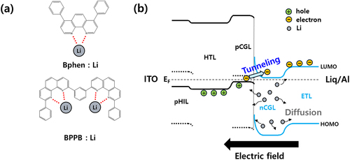
Figure (b) depicts the energy level alignment and charge transport mechanism in a typical CGL device structure, which comprises organic heterojunction with pCGL and nCGL. pCGL contains high concentrations of deep-lying LUMO material where holes are generated on the highest occupied molecular orbitals (HOMOs) of HTL, and electrons are generated on the LUMOs of p-dopant through intermolecular charge generation. Due to high charge concentration, there is intense band-bending and narrow depletion region at the heterojunction. When a reverse bias is applied to the CGL device, the electrons generated on the LUMO of p-dopant are easily tunneled into the LUMO of the nCGL layer assisted by the gap states that come from metal–organic coordination reaction and transported to the electrode [Citation23,Citation24], which is the same electrical-driven condition of CGL in the typical stacked device. If Li were to diffuse into adjacent layers by concentration gradient or external stress, the electronic structure of the CGL device may change, degrading its electronic properties.
To investigate the deterioration of Li-doped CGL with Phen-based ETMs, two types of the same four CGL devices were fabricated with the structure of ITO/ NDP-9 3 wt.% doped BCFN (10 nm)/ BCFN (60 nm)/ NDP-9 10 wt.% doped BCFN (10 nm)/ Li 5 wt.% doped ETM (10 nm)/ ETM (30 nm)/ Liq (1.5 nm)/ Al (100 nm), where NDP-9 is 2-(7-dicyanomethylene-1,3,4,5,6,8,9,10-octafluoro-7H-pyrene-2-ylidene)-malononitrile as a p-dopant, and BCFN is N-([1,1'-biphenyl]−4-yl)−9,9-dimethyl-N-(4-(9-phenyl-9H-carbazol-3-yl)phenyl)−9H-fluoren-2-amine as a hole transport material and ETM is Bphen or BPPB, respectively. The frontier orbital level of materials used in this study was measured by differential pulse voltammetry and is represented in Figure S2. Moreover, to explore which stress is critical for CGL degradation, the CGL devices were exposed to stresses that are slightly more stressful than the general OLED device operating conditions: constant current density (J – stress) of 25 mA/cm2, thermal stress of 40°C (T – stress), and both current and thermal stress at the same time (J–T–stress). For comparison, one device was left in ambient conditions without any stress. Measurements were conducted at room temperature every 30, 70, and 160 hours during stress application.
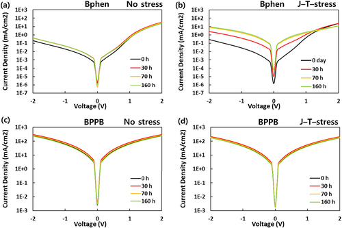
Figure describes the current density – voltage characteristics of CGL devices with Bphen and BPPB as ETM under no stress and J–T–stress, respectively. The results according to J – stress and T – stress are in Figure S3. The CGL device produced symmetrical current properties at forward and reverse bias, indicating high conductivity and an efficient tunneling process. In the CGL device, the low electric field in reverse bias between 1 V ∼ 0 V range is related to tunneling, and the higher electric field is regarded as trap-assisted space charge – limited current region approximated by a power law: J ∼
where n > 2 [Citation25,Citation26]. As presented in Figures (a and c), the storage conditions do not impact the electrical properties of CGL devices much. In the case of the CGL device with Bphen, the current density of J – stressed device at
1 V increased 8.3 times after 160 h aging time, while that of the T-stressed device increased 33.8 times at the same bias. Additionally, the current density of the J–T–stressed device significantly increased 80.1 times, implying that simultaneous J – stress and T-stress accelerate to change electrical characteristics. While CGL devices with Bphen exhibited a relatively large discrepancy of J – V characteristics, a slight difference was observed depending on the stress condition in the CGL devices with BPPB, which was insufficient to distinguish how the electrical properties have been changed according to aged devices. The reason why the curve shape differs in CGL devices with Bphen is discussed later.
Figure 2. The current density (J) – voltage(V) characteristics of CGL devices with Bphen and BPPB according to aging time and stress condition. (up) Bphen as ETM, (down) BPPB as ETM, (left) no stress, (right) J – T – stress.
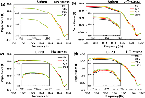
To investigate electrical properties in detail, impedance spectroscopy, a versatile tool that discerns the electrical properties of organic semiconductors non-destructively, was carried out. Figure and Figure S4 demonstrate the capacitance – frequency characteristics of CGL devices at 0 V according to various stress conditions and aging time. The CGL device can be represented with an equivalent circuit comprising series and parallel resistances and capacitors. Since pCGL and nCGL are highly conductive due to high charge density, both layers act as pseudo-electrode; thus, it can be deduced that the capacitance in the low-frequency region is contributed by the depletion region. One can conclude that the capacitance in the low-frequency region is responsible for the dielectric relaxation of impurities during fabrication or the formation of additional deep trap states. [Citation27–29] However, all devices were fabricated simultaneously without breaking the vacuum, and the no-stress devices barely changed according to the aging time. Hence, the possibility of those factors can be excluded. Meanwhile, the high-frequency range is responsible for the response of the relaxation and redistribution of contact and organic transport layer. When it comes to the low-frequency region around 10 Hz ∼ 0.1 MHz, the J – stressed devices regardless of ETM showed almost little or no difference similar to the no-stress devices. However, the T – stressed devices and the J–T–stressed devices gradually increased in capacitance at the same frequency range, suggesting that T – stress is responsible for the increase of capacitance in the low frequency range. The capacitance of the J – T-stress devices changed mostly and also seems to sum the variation of the J – stressed and the T – stressed devices. Moreover, considering the relationship between capacitance and depletion width (W), C = ϵ0ϵrA/W where ϵ0, ϵr, and A are vacuum permittivity, dielectric constant, and pixel area, respectively, the depletion width became narrower as thermal stress is applied. In the high-frequency region over 0.1 MHz, J – stress and J–T–stress devices decreased in capacitance, while that of the T – stress devices scarcely changed. Combining the J – V and capacitance – frequency characteristics suggests that J – stress and T – stress affect the change of electrical properties to the CGL device differently.
Figure 3. Capacitance – frequency data of the CGL devices at 0 V with Bphen and BPPB according to aging time and stress conditions. (up) Bphen as ETM, (down) BPPB as ETM, (left) no stress, (right) J – T – stress. The inset figures display a zoomed-in view in 10 Hz and 0.1 MHz range.
As the electron tunneling from pCGL to nCGL occurs via trap states formed by a coordination reaction between Li and ETM [Citation24,Citation25,Citation30], the variation of trap density and trap energy would impact the electrical properties of CGL. In disordered organic molecules, the trap property is described by exponential expression with the assumption of Gaussian distribution of the density of state (DOS), which is given by Equation 1[Citation31,Citation32]:
(1)
(1) H(E) is the trap density of states (DOS) at the energy level E, Ht is the total trap DOS, and Et is the characteristic energy of trap distribution that has a relationship with characteristic temperature Tc (Et = kTc), where k is the Boltzmann constant. The exponential trap distribution model results in current density – voltage characteristics, as specified in Equation 2:
(2)
(2) where q, µn, and Nc are the elementary charge, the carrier mobility, and the DOS in the relevant band, respectively, l = Tc/T, and d is the sample thickness. In the case of l > 2, Equation 2 can be expressed in Arrhenius dependence and be written as
(3)
(3) where J0 is constant and the activation energy, Ea = kTcln(qd2Ht/2ϵ0ϵrV). Furthermore, Equation Equation3
(3)
(3) states a temperature temperature-independent current at a crossover voltage Vt, where Ea is zero, and
(4)
(4) To further elucidate the change of electrical characteristics of degraded CGL devices according to different aging conditions, we measured temperature-dependent J – V characteristics of 160 h aged CGL devices and extracted Ea, Et, and Ht by fitting the experimental data using the above equations. Figure details the relevant fitting results of the J–T–stress device with Bphen and BPPB. The results at the other stress conditions are represented in Figures S5–S6, and the parameters are summarized in Table . ϵr for BPPB and Bphen device was obtained to be 3.58 and 3.8, respectively, by measuring the capacitance-frequency of the CGL devices (see Figure S6). All aged devices showed similar temperature-dependent current density characteristics, as depicted in Figures (a and d). For analysis, we selected the current density at – 2 V to investigate the tunneling characteristics. Since it is well known that the trap model of space charge – limited current is valid in the high-temperature range [Citation33], linear fitting of ln(J) – 1/T curves was carried out in the range from 200 K to 275 K, as in Figures (b and e). The calculated Ea decreases, regardless of ETM when the external stresses are applied. In addition, it is notable that the T – stress has a greater impact on Ea than J – stress. In the case of Et, a significant change was observed in J – stress and J–T–stress devices with Bphen, while the devices with BPPB showed little difference. This decrease of Et in the Bphen devices seems to be in line with capacitance characteristics at the high-frequency range, which is responsible for charge transport ability. As shown in Figures (c and f), the temperature-independent voltage, Vt gives information on the trap density Ht. Interestingly, the calculated Ht values decrease over external stress in both CGL devices with Bphen and BPPB. However, the J–T–stress device with Bphen reduces Ht by 72%, whereas the device with BPPB demonstrates a comparatively lower decrease of Ht by 26%. Since the p-dopant is expected to be more stationary than Li for its heavier molecular weight (472 g/mol), the Li diffusion in nCGL might be the key factor influencing the variation of these electrical characteristics.
Figure 4. Temperature-dependent characteristics of 160 h aged CGL device at 40°C (up) Bphen device, (down) BPPB device. (a), (d) J – V data from 77 K to 275 K, (b), (e) ln(J) – 1000/T data at – 2 V. (c), (f) J – V data from 200 K to 275 K, and the black lines are the extrapolation in the high voltage region.
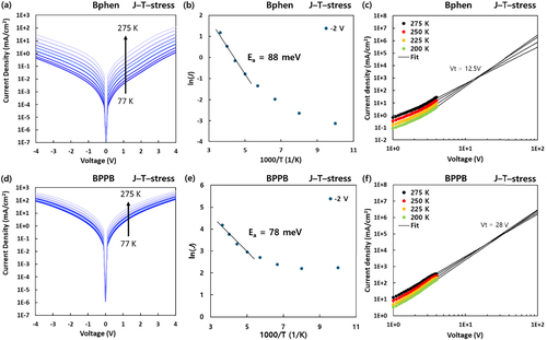
Table 1. Ea at – 2 V, Et at 275 K, and Ht of 160 h aged CGL devices with Bphen and BPPB according to stress conditions.
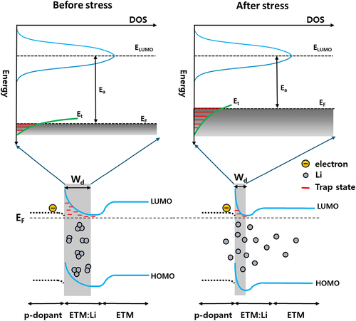
Interestingly, the increase in current density around the low voltage region, increase in capacitance at the low-frequency range, and decreased Ea according to the external stress imply that the electrical properties of CGL devices with Phen – based ETMs were improved, especially in tunneling. This enhanced tunneling property after stress means reducing depletion width at the CGL interface. Figure differentiates the change of electronic energy levels at the Li-doped nCGL before and after stress. The electrons generated on the LUMO of p-dopant are tunneled through the depletion region by filling the trap states in the depletion region. When the nCGL is constructed during fabrication, Li is evaporated in the form of cluster type so that there may be a lesser number of chemical bonds per unit volume. After that, Li is redistributed, driven by the concentration gradient, and particularly mild thermal stress may alter the morphology of the CGL layer, encouraging the redistribution. Accordingly, the actual interaction between N sp2 orbital and Li increases, leading to a narrower depletion width. As more trap states are filled by increased free charge carrier, Ea and the trap density that electrons should hop for tunneling also decrease for the narrow depletion width.
Figure 5. (up) The enlarged schematic diagram of the electron transport DOS assuming Gaussian distribution and trap energy level, (down) interface energy level diagram p-dopant/Li-doped ETL/ETL before and after stress.
Overall, the electrical characteristics of the devices with Bphen have undergone more significant changes than the devices with BPPB. To understand the binding nature between nCGL (BPhen and BPPB) and Li, the density functional theory (DFT) calculations were carried out, employing Becke’s three parameterized Lee–Yang–Parr exchange functionals (B3LYP) with 6-311G** basis set, as implemented in the suite of Gaussian 09 program [Citation34]. In addition to this, Grimme’s dispersion correction with Beckes-Johnson sampling (GD3BJ) was considered to describe the non-covalent interaction due to the lack of van der Waals terms in B3LYP functional. Before computing the Li coordinated nCGL structures, two isomers of BPPB should be compared to identify the stable one (See Figure S8). To compare the energies of these isomers, the potential energy surface (PES) calculation, along with the dihedral angle between bridged phenyl and phenanthroline moieties, was conducted. As portrayed in Figure S9, the helical form is approximately 0.38 eV more stable than the S-shaped form, indicating that the helical form is the most stable form of BPPB material. Based on this calculation, we further computed the Li-coordinated Bphen and BPPB structures (Bphen:Li and BPPB:Li). Figure S10 denote that Li is tetradentately coordinated to BPPB, while it is bidentately coordinated to Bphen. Hence, BPPB may show a stronger binding energy. To quantitatively compare the binding strength between nCGLs and Li, we computed the binding energies of Bphen:Li and BPPB:Li, which are calculated to be 2.474 and 2.799 eV, respectively. This result indicates that Li is strongly coordinated with BPPB rather than Bphen. Unlike Bphen, it is further noticed that two Li atoms can maximally bind to BPPB with a binding energy of 4.899 eV. Therefore, BPPB seems to be advantageous in suppressing Li diffusion. The other factor that may affect Li diffusion is molecular packing; that is, the more porous the film is, the more likely metal diffuses through the interstitial sites. This geometric characteristic of the molecule is reflected in photoluminescence (PL) spectra, as represented in Figure S11. The film PL spectrum of BPPB exhibited a large bathochromic shift compared to that of Bphen, indicating that the molecular packing would be more dense in BPPB than Bphen.
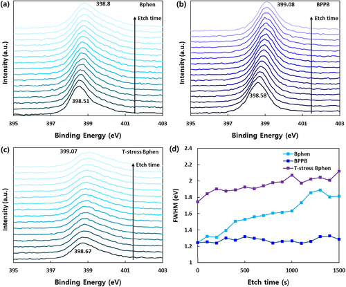
To further investigate the Li diffusion, we prepared films with a structure of Si wafer/ 5 wt.% Li:ETMs (10 nm)/ETMs (40 nm), where ETMs are Bphen and BPPB, and X-ray photon spectroscopy (XPS) depth profiling was performed a day after fabrication. The XPS spectra of the N 1s core level according to etch time are exhibited in Figure (a and b). The peak binding energy of intrinsic Bphen and BPPB is shifted toward higher energy as the etching time increases, demonstrating the effect of the coordination reaction between Li and ETM [Citation19,Citation35] The actual binding energies of Bphen and BPPB in the solid state are 0.29 and 0.5 eV, respectively, calculated from the difference between the peak binding energy of pristine and 1500 s etched film, which agree with computed binding energies of Bphen:Li and BPPB:Li. Since the full width at half maximum (FWHM) of N 1s core spectra is proportional to the number of chemical bonds between Li and N atom, the change of FWHM of the spectra can be interpreted as the diffusion of Li. Figure (d) shows the FWHM of the N 1s core spectra of Bphen and BPPB films according to etch time. Surprisingly, the Bphen film gradually broadened the spectrum during etching, while the BPPB film kept a consistent spectral shape. These results reveal that the Li easily diffuses in the Bphen rather than BPPB. Moreover, the thermal effect on Li diffusion was also investigated in the T – stress Bphen film. The film was heated at 40°C for 5 hours in an N2-filled glove box to prevent oxidation. The entire XPS spectra were slightly shifted toward higher binding energy compared to non-stressed film and were significantly broadened. In Figure (d), the FWHMs of the T – stress Bphen film were much larger than those of non-stressed film and increased up to 2.12 eV, which ascertains that temperature even under Tg facilitates cleavage of the weak coordination interaction between Li and the ring sp2 nitrogens and that the free Li can swim within the sparse matrix more easily.
Figure 6. XPS depth profile of partially Li – doped (a) Bphen, (b) BPPB films, (c) T – stressed Bphen film, and (d) FWHM of N 1s core spectra according to etch time.
Returning to Figure , the reason for the different J – V curve shapes of the CGL device with Bphen can be explained by considering experimental results. When it comes to the interface between intrinsic ETL and Liq/Al, there is a coordination reaction between Liq/Al and phenanthroline moiety because diffusion of Li and Al into ETL occurs as well [Citation22]. Therefore, it can be expected that Bphen has a relatively higher Schottky barrier than BPPB, so the Bphen CGL device shows asymmetric current density characteristics at forward bias. However, as Li/Al diffuses into Bphen ETL after aging, the ohmic contact at the interface is formed, which facilitates electron injection at forward bias. That is why the current density curve of the Bphen CGL device became a ‘V’ shape gradually according to aging time. However, the BPPB CGL device where metal diffusion is not favorable exhibits no difference in a line shape. In addition, the electron mobility of Bphen is 1 order lower than that of biphenanthroline-based materials [Citation24]. Considering the morphological properties that are responsible for charge transport ability together, a lower current density is expected for the Bphen CGL device.
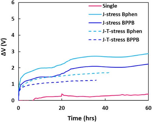
Based on the results that BPPB is more stable than Bphen in response to changes in the CGL device electrical characteristics induced by Li diffusion, we fabricated a single EL unit and double-stacked tandem OLEDs to evaluate whether the same results of Li diffusion depending on the host material of nCGL were observed in the EL devices. The detailed device structures are described in the Experimental section in Supporting Information. The EL properties of three devices are shown in Figure S12 and synthesized in Table S1. The current density of the BPPB tandem device was higher than that of the device with Bphen due to the enhanced electron mobility originating from π – π stacking of biphenanthroline. The driving voltage at 25 mA/cm2 of the Bphen tandem and BPPB tandem device was almost twice that of the single EL device, which means the CGL connects the two EL units without electrical resistance. Notably, the current efficiency of the two tandem devices was slightly less than twice that of the single device due to the different EL spectrum. The devices were aged under J – stress and J–T–stress and relative luminance data are illustrated in Figure S13. Despite higher initial luminance (L0), the tandem devices exhibited a much longer device lifetime than the single EL device under the same J – stress. Specifically, the device lifetime of the BPPB device is longer than that of the Bphen device. Moreover, the change in operating voltage showed a clear discrepancy between Bphen and BPPB devices as shown in Figure . The operating voltage of the Bphen device increased gradually to a greater extent compared to the BPPB device, which can be interpreted as a result of the degradation phenomenon of CGL, and ultimately, can be seen as a result of differences in Li diffusion.
Figure 7. The change of the operating voltage of single and tandem devices with Bphen and BPPB as an nCGL material under J – stress and J – T – stress.
Conclusion
In summary, the degradation characteristics of Li – doped CGL with phenanthroline – based ETMs were investigated comprehensively under various stress conditions. The exponential trap distribution model analysis via temperature-dependent current density – voltage characteristics confirmed the change of electrical properties of nCGL is ascribed to the diffusion of Li. In particular, thermal stress impacts the reducing depletion width within CGL, and the current stress affects charge transport properties. Additionally, XPS depth profiling evidenced the diffusion phenomenon of Li, and the thermal effect on Li diffusion was also verified. In molecular scope, the more sparsely the molecule is packed, the easier Li diffuses, revealing that the stability of BPPB against Li diffusion is superior to that of Bphen. It was also confirmed in tandem OLEDs when Bphen and BPPB were adapted as nCGL hosts. Consequently, we expected that these results would pave the way to understanding the degradation of tandem OLED and constructing a stable and efficient nCGL host.
Disclosure statement
No potential conflict of interest was reported by the author(s).
Additional information
Funding
Notes on contributors

Ki Ju Kim
Ki Ju Kim received his B.S. (Chemical Engineering) and M.Sc. (Information Display Engineering) from Hongik University, the Republic of Korea, in 2019 and 2021, respectively. He is now pursuing a Ph.D. in Information Display Engineering at Hongik University. His research interests include device – and photo-physics of various OLEDs and their applications for near-eye and transparent displays.

Sunwoo Kang
Sunwoo Kang received his Ph.D. from the Department of Chemistry at Sungkyunkwan University under the supervision of Prof. Jin Yong Lee in 2012. From 2013 to 2024, he worked at Samsung Display’s Research Center. He is now an assistant professor at Dankook University. His research interests have primarily centered on understanding the underlying optoelectronic property of blue-emissive material at the molecular level.
Taekyung Kim
Taekyung Kim received his B.S. from Seoul National University in 2000, and his M.S. and Ph.D. from the University of Illinois at Urbana-Champaign in 2003, and 2007, respectively. From 2007 to 2010, he was a postdoctoral associate at the Sandia National Labs, NM, USA. He joined Samsung Display in 2010 and has been an associate professor at Hongik University since 2019. His research interests include the degradation mechanism in OLEDs and the development of novel analysis methodologies for various OLEDs.
References
- H. Cho, C.-W. Byun, C.-M. Kang, J.-W. Shin, B.-H. Kwon, S. Choi, N.S. Cho, J.-I. Lee, H. Kim, and J.H. Lee, J. Inf. Disp. 20, 249–255 (2019). doi:10.1080/15980316.2019.1671240
- H.J. Jang, J.Y. Lee, G.W. Baek, J. Kwak, and J.-H. Park, J. Inf. Disp. 23, 1–17 (2022). doi:10.1080/15980316.2022.2035835
- L. Liao, K.P. Klubek, and C.W. Tang, Appl. Phys. Lett. 84, 167–169 (2004). doi:10.1063/1.1638624
- K.S. Yook, S.O. Jeon, S.Y. Min, J.Y. Lee, H.J. Yang, T. Noh, S.K. Kang, and T.W. Lee, Adv. Funct. Mater. 20, 1797–1802 (2010). doi:10.1002/adfm.201000137
- C.-C. Chang, J.-F. Chen, S.-W. Hwang, and C.H. Chen, Appl. Phys. Lett. 87, 253501 (2005). doi:10.1063/1.2147730
- L.-S. Liao, W.K. Slusarek, T.K. Hatwar, M.L. Ricks, and D.L. Comfort, Adv. Mater. 20, 324–329 (2008). doi:10.1002/adma.200700454
- Y. Dai, H. Zhang, Z. Zhang, Y. Liu, J. Chen, and D. Ma, J. Mater. Chem C 3, 6809–6814 (2015). doi:10.1039/C4TC02875A
- H. Sun, Q. Guo, D. Yang, Y. Chen, J. Chen, and D. Ma, Acs Photonics 2, 271–279 (2015). doi:10.1021/acsphotonics.5b00010
- W.-h. Park, D.-p. Park, and S.S. Kim, J. Inf. Disp. 23, 45–52 (2022). doi:10.1080/15980316.2021.1947403
- J. Park, K.J. Kim, J. Lim, T. Kim, and J.Y. Lee, Adv. Mater. 34, 2108581 (2022). doi:10.1002/adma.202108581
- H. Kanno, R.J. Holmes, Y. Sun, S. Kena-Cohen, and S.R. Forrest, Adv. Mater. 18, 339–342 (2006). doi:10.1002/adma.200501915
- M.-Y. Chan, S.-L. Lai, K.-M. Lau, M.-K. Fung, C.-S. Lee, and S.-T. Lee, Adv. Funct. Mater. 17, 2509–2514 (2007). doi:10.1002/adfm.200600642
- K. Hong, and J.-L. Lee, J. Phys. Chem C 116, 6427–6433 (2012). doi:10.1021/jp212090b
- J. Liu, Y. Chen, D. Qin, C. Cheng, W. Quan, L. Chen, and G. Li, Semicond. Sci. Technol. 26, 095011 (2011). doi:10.1088/0268-1242/26/9/095011
- S. Hamwi, J. Meyer, M. Kröger, T. Winkler, M. Witte, T. Riedl, A. Kahn, and W. Kowalsky, Adv. Funct. Mater. 20, 1762–1766 (2010). doi:10.1002/adfm.201000301
- C.-W. Chen, Y.-J. Lu, C.-C. Wu, E.H.-E. Wu, C.-W. Chu, and Y. Yang, Appl. Phys. Lett. 87, 241121 (2005). doi:10.1063/1.2141718
- J. Li, C.W. Rochester, I.E. Jacobs, S. Friedrich, P. Stroeve, M. Riede, and A.J. Moule, ACS Appl. Mater. Interfaces. 7, 28420–28428 (2015). doi:10.1021/acsami.5b09216
- B. Lüssem, M. Riede, and K. Leo, physica status solidi (a) 210, 9–43 (2012). doi:10.1002/pssa.201228310
- G. Parthasarathy, C. Shen, A. Kahn, and S.R. Forrest, J. Appl. Phys. 89, 4986–4992 (2001). doi:10.1063/1.1359161
- F.A. Angel, J.U. Wallace, and C.W. Tang, Org. Electron. 42, 102–106 (2017). doi:10.1016/j.orgel.2016.12.023
- Y. Lu, Z. Liu, Y. Zhang, C. Zhang, J. Wei, Z. Bin, X. Wang, D. Zhang, and L. Duan, CCS Chemistry 3, 367–376 (2021). doi:10.31635/ccschem.021.202000611
- T. Sasaki, M. Hasegawa, K. Inagaki, H. Ito, K. Suzuki, T. Oono, K. Morii, T. Shimizu, and H. Fukagawa, Nat. Commun. 12, 2706 (2021). doi:10.1038/s41467-021-23067-2
- J.-P. Yang, F. Bussolotti, Y.-Q. Li, X.-H. Zeng, S. Kera, J.-X. Tang, and N. Ueno, Org. Electron. 24, 120–124 (2015). doi:10.1016/j.orgel.2015.05.033
- G.W. Kim, Y.H. Son, H.I. Yang, J.H. Park, I.J. Ko, R. Lampande, J. Sakong, M.-J. Maeng, J.-A. Hong, J.Y. Lee, Y. Park, and J.H. Kwon, Chem. Mater. 29, 8299–8312 (2017). doi:10.1021/acs.chemmater.7b02655
- D. Ma, and Y. Chen, Organic Semiconductor Heterojunctions and Its Application in Organic Light-Emitting Diodes (Springer, 2017).
- S. Lee, J.H. Lee, J.H. Lee, and J.J. Kim, Adv. Funct. Mater. 22, 855–860 (2011). doi:10.1002/adfm.201102212
- S. Nowy, W. Ren, J. Wagner, J.A. Weber, and W. Brütting, Proc. SPIE 7415, Organic Light Emitting Materials and Devices XIII, 74150G (2009). doi:10.1117/12.824856
- H. Lee, K.J. Kim, Y.J. Moon, Y.K. Kim, and T. Kim, Org. Electron. 84, 105816 (2020). doi:10.1016/j.orgel.2020.105816
- L. Burtone, J. Fischer, K. Leo, and M. Riede, Phys. Rev. B 87, 045432 (2013). doi:10.1103/PhysRevB.87.045432
- Y.-H. Lee, M.-W. Lin, T.-C. Wen, and T.-F. Guo, J. Appl. Phys., 114 (2013).
- M. Kuik, G.J.A. Wetzelaer, H.T. Nicolai, N.I. Craciun, D.M. De Leeuw, and P.W. Blom, Adv. Mater. 26, 512–531 (2014). doi:10.1002/adma.201303393
- Q. Guo, D. Yang, J. Chen, X. Qiao, T. Ahamad, S.M. Alshehri, and D. Ma, J. Appl. Phys. 121, 115502 (2017). doi:10.1063/1.4978609
- V. Kumar, S. Jain, A. Kapoor, J. Poortmans, and R. Mertens, J. Appl. Phys. 94, 1283–1285 (2003). doi:10.1063/1.1582552
- M. Frisch, G. Trucks, H. Schlegel, G. Scuseria, M. Robb, J. Cheeseman, G. Scalmani, V. Barone, B. Mennucci, and G. Petersson, Inc., Wallingford CT (2009).
- M.S. Ki, M. Sim, O. Kwon, K. Im, B. Choi, B.J. Cha, Y.D. Kim, T.Y. Jin, and K. Paeng, ACS Mater. Lett. 4, 1676–1683 (2022). doi:10.1021/acsmaterialslett.2c00583