
 ?Mathematical formulae have been encoded as MathML and are displayed in this HTML version using MathJax in order to improve their display. Uncheck the box to turn MathJax off. This feature requires Javascript. Click on a formula to zoom.
Abstract
To get enhanced long-wavelength absorption, an impurity photovoltaic (IPV) mechanism was implemented within a transparent conducting oxide (TCO) at the rear of a solar cell. The numerical simulation of the N+/P (silicon)/IPV-TCO device was carried out by using SCAPS-1D program which allows the inclusion of optically active defects. In the proposed heterostructure configuration, ZnTe is a suitable material as back surface reflector. In analyzing the Si/ZnTe interface, lattice mismatch, energy band alignment and defects density were considered with appropriate treatment. In particular, to cure the detrimental 12% lattice mismatch at the interface, a thin silicon amorphous layer was inserted in-between, allowing 22.98% conversion efficiency. With adapted ZnTe Lucovsky's model for the optical capture cross sections and introduction of an oxygen radiative IPV defect (O2 level at 0.4 eV below the conduction band), a conversion efficiency of 27.15% was ultimately achieved. The experimental feasibility of the high-efficiency heterostructure device is evaluated.
1. Introduction
The stagnation of the conversion efficiency of silicon-based solar cells for more than two decades has led to the search for new concepts and adapted materials. Great expectations come from forefront technologies that are being developed continuously to improve the conversion efficiency. One is the design of the well-known HIT (heterojunction with intrinsic thin layer) structure, which gives interesting insights about the prominent passivating base layer through its interfacing with ultra-thin doped amorphous silicon [Citation1]. Despite an efficiency exceeding 26%, the HIT technology is hindered by a higher wafer price and rather complex passivating processes. Another recent device architecture is based on a Perovskite/Silicon tandem technology considered as a cost-effective approach to realize a cell efficiency of 28% [Citation2]. However, the major challenges for this combination are the short and long-term device stability and an observed hysteretic current–voltage characteristics. An alternate route to further increase the efficiency can be achieved by the optimal exploitation of the solar spectrum, through recovering the incident photons whose energy is lower than the bandgap. This mechanism known as impurity photovoltaic (IPV) effect has been investigated by many authors [Citation3,Citation4]. It consists of absorbing sub-bandgap photons by introducing one or more impurity energy levels in the semiconductor bandgap. Spatial location of the suitable impurity traps within the gap, doping level and compensation of charges caused by the traps are recognized as requirements to get effective IPV effect. Indeed, as deep defect states can act at the same time a destructive role as recombination centres, the open-circuit voltage can be reduced drastically by adverse effect of the dark current increase [Citation5]. Furthermore, to minimize carrier losses at the rear side of the device, the conventional configuration should include a back surface field (BSF). Besides, to insure IPV effect advantage, high light trapping (close to 100%) both at the front and at the rear part of the device is essential to insure effective gains in quantum efficiency [Citation6].
The highlight of IPV effect has been addressed by the introduction of various impurities in crystalline silicon substrates. Considering a n+/p/p+ IPV Si solar cell doped with Tellurium (trap level Et at 0.14 eV below the conduction band edge), J. Yuan et al. investigated the impurity concentration level and the light trapping coefficient on the cell performance. They theoretically demonstrated a net increase of 2.79% for conversion efficiency by using the IPV effect [Citation7]. R. Sircar et al. have studied a p+/n/n+ solar cell doped with Indium, Thallium and Vanadium, which have Et at 0.157, 0.26 and 0.36 eV above the maximum valence band edge, respectively. Cell efficiency improvement with 3% of Vanadium was obtained, which is mainly due to the extension of the infrared response [Citation8]. The problems associated with the conventional IPV effect in the silicon substrate are related to new recombination paths while introducing states in the band gap and parasitic absorption. To overcome these issues, one can consider the possibility of isolating the impurity level within a larger bandgap material located at the backside of the cell. In fact, the idea had arisen from the work of D. Macdonald et al. [Citation9] stipulating that better results might be achievable with materials other than the combination of amorphous and crystalline silicon. Thus, rather than using amorphous silicon, we consider in our study a transparent conducting oxide (TCO) material having comparable bandgap and electron affinity (1.72 and 3.80 eV, respectively). The higher bandgap will induce an energy band offset capable to repeal the minority carriers generated in the lower doped silicon base. It also prevents their recombination through the IPV effect located within the TCO. ZnTe thin layer is one possible candidate, already implemented successfully as a conduction band barrier and back reflector in high-efficiency CdTe based solar cells [Citation10,Citation11]. With a direct bandgap of ∼ 2.26 eV with a zinc-blend crystal structure, ZnTe exhibits a high p-type electrical conductivity with controllable hole concentration as high as 1020 cm−3 when doped with nitrogen [Citation12]. If this latter property is compliant with expected efficiency improvement as BSF, ZnTe wide bandgap with a low electron affinity value (3.53 eV) is not a priori a suitable partner material with silicon. Thus, one of the first tasks to undertake in our study will be to manage the lattice mismatch and the energy band alignment between the two adjacent materials.
We report in this contribution, the numerical analysis of n+/p/p+ Si solar cells with particular emphasis on the p+ back ZnTe layer hosting an IPV defect and discuss the results comparatively with those obtained with a conventional silicon solar cell. At the end of the study, the possibilities of technological implementation of the new structure are discussed.
2. IPV cell structure and theoretical details
For a concise presentation, the fundamentals of IPV theory will not be detailed herein and useful developments can be found in the literature [Citation13,Citation14]. We will just recall the most relevant features of this mechanism enabling creation of additional electron–hole pairs by a 2-step absorption via electronic states located within the bandgap of the base. These features are: modified Shockley-Read-Hall model, optical emission rates from the impurity for electrons and holes, spatial position of the impurity energy level from the edge of the conduction (or valence) band and impurity concentration Nt. The IPV Si solar cell under study is an n+/p/p+ structure with a donor-type impurity confined only in the p-base. The n+ front region is a conventional thin Si diffused emitter, whereas the rear highly p+ doped layer can be either boron-doped silicon or a ZnTe thin film. To highlight the IPV effect, various doping elements (Te, Mg, Se, …) have been investigated in the literature. In the frame of this work, we merely consider a single impurity that it is very near the bottom of the conduction band ([Ec – Et] ∼ 0.20 eV) with variable concentration. The carrier's photoemission cross-sections are evaluated according to Lucovsky's model [Citation15]. Internal reflection coefficients at the front (Rf) and at the back (Rb) of the device are assumed close to unity.
Owing to heterojunction configuration including interfaces with unmatched lattices and complex mechanisms, a prior approach through accurate parameter modelling and device simulation is necessary anticipate its performance characteristics, provide physical insight and ultimately help to assist a process manufacturing. Numerical calculations are performed by the one-dimensional SCAPS v.3.3.03 simulator developed at the University of Gent, Belgium [Citation16]. This software is a Windows-oriented program, developed with LabWindows/CVI of National Instruments and dedicated to thin film solar cells. It enables the definition of a stack of semiconductor layers, the assignment of material properties to each layer and the possibility to introduce multiple defects states in the bulk of films and at the interfaces. Among various others programs (AFORS-Het [Citation17], Amps-1D [Citation18], Silvaco/Atlas – 2D [Citation19]) the choice of SCAPS was motivated by the fact that is, to our knowledge, the only software that includes models for the IPV mechanism. The software solves numerically in steady state the system of differential equations that govern the carrier transport, namely the coupled Poisson (1) and continuity equations for electrons and holes (2):
(1)
(1) where ψ is the electrostatic potential, q is the electron charge, ε is the permittivity of the material, n and p are the electron and hole densities,
and
are the shallow acceptor and donor ionized concentrations, nt and pt are the trapped electron and hole concentrations.
For the continuity equations, Jn and Jp represent the electron and hole current densities respectively, which are based on the drift-diffusion model:
(2)
(2)
U is the net electron–hole recombination rate including radiative, Auger, multiple deep trap levels and impact ionization mechanisms. Recombination through multiple deep-trap levels in the bandgap is described by the Shockley–Read–Hall theory [Citation20]. Finally, G(x) is the solar-induced carrier generation rate at a distance x below the exposed semiconductor surface.
The electron and hole current densities depend on the gradient of the corresponding quasi-Fermi levels EFn and EFp according to:
(3)
(3)
μn and μp are the electron and hole mobilities.
The prevailing conditions are 300°K, AM1.5G standard light spectrum at steady-state conditions (n/
,
p/
t = 0). For the front and the back contact, the only variables are the work function and the barrier level. At the interface between metal and semiconductor, the model implemented for transport of majority carriers is thermionic emission. Furthermore, optical capture of electrons and holes, internal light trapping schemes are implemented in the programme. For the modelled device, the donor-type defect concentration is 9.1016 cm−3, close to base doping concentration.
The parameters used for simulations of the heterostructure Si-based solar cell are summarized in Table . For the sake of precision, the values used are for the most part based on experimental results. For the p+ silicon back layer (not reported in the table), one considers a thickness and doping concentration of 1 µm and 1018 cm−3 respectively with all other settings identical to the p-silicon material layer.
Table 1. Physical properties of materials used in simulation.
Optical properties of ZnTe are based on the study of K. Sato and S. Adachi [Citation21]. The IPV mechanism was evaluated through the determination of the electron and hole optical cross section σn,p of the impurity [Citation15]:
(4)
(4) For the above expression, one needs the knowledge of n*, the refractive index of the host material, the effective field ratio
for the radiation inducing the transition, the effective mass
of the carriers and the ionization energy of the impurity Ei relative to the bottom (top) of the conduction (valence) band. c is the velocity of light. The asterisk * assigned to the refractive index (n*) was used to differentiate it from the electron concentration n.
All these parameters have to be introduced in the defect properties panel of the SCAPS program. In particular and for silicon host material, the effective field ratio has been approximated for minority carriers as [Citation22]:
(5)
(5) For other materials, this ratio can be evaluated from the following Dexter's expression [Citation23]:
(6)
(6)
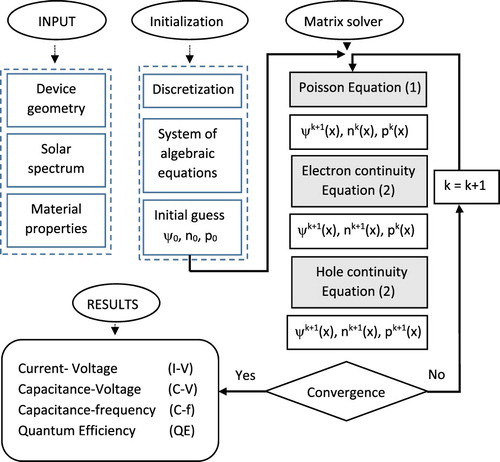
The flow diagram of the simulation process is shown in Figure . With appropriate boundary conditions at the interfaces and at the contacts, the code solves at each point of a discretized network the above one-dimensional equations (1)–(2) using a Gummel iteration scheme with Newton–Raphson sub-steps [Citation24]. Unknowns are electrostatic potential (ψ) and carrier concentrations (n and p).
Figure 1. Flowchart of the algorithm implemented in the simulation code.
3. Results and discussion
3.1. Validating the IPV effect on usual n+/p/p+ silicon device
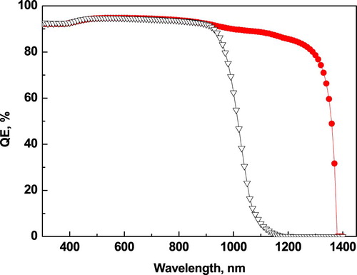
The all silicon n+/p/p+ device without IPV effect exhibits a power conversion efficiency (PCE) of 22.65%, with an open circuit voltage (Voc) = 0.746 V, a short circuit current (Jsc) = 36.73 mA/cm2 and a fill factor (FF) = 82.69%. These performance values are close to that of recent best industrial silicon-based solar cells with a PCE = 21.25% [Citation25]. With IPV introduction, the efficiency is enhanced to 26.05% (+3.4% absolute) due to strong Jsc increase, but with a Voc and FF slight degradation (to 0.711 V and 77.24%, respectively). The PCE gain obtained is within the range of values reported in the introduction section and for a variety of dopants. The short circuit current increase is a consequence of the quantum efficiency expansion, noticeable in the 900–1400 nm range through the IPV effect (Figure ). After J. Yuan et al [Citation7], when the impurity concentration Nt is close but lower than the base doping concentration (Nt ≤ NA), the impurity level is fully emptied; then sub-bandgap photons can be absorbed by the electron photoemission process from the valence band to the defect level, giving rise to the enhanced current density. The slight decrease of Voc is imputed to the Te impurity concentration close to that of Si base doping (1×1017 cm−3), which enhances the recombination process through the defect [Citation26]. In this case, the free-carrier concentration is reduced and consequently the conductivity of the base region; this effect is similar to that of a series resistance which lessens the fill factor [Citation27].
Figure 2. Quantum efficiency of silicon solar cell with (![]()
3.2. Insertion of the undoped ZnTe and Mo-doped ZnTe back layer
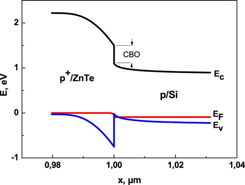
By replacing the rear 1 µm p+ silicon layer by a 100 nm ZnTe thin film (Eg = 2.26 eV; χ = 3.53 eV), the first numerical results shows either negligible conversion efficiency or a convergence failure, explained by the large bandgap discrepancy and relatively high conduction band offset (CBO ≈ 0.4 eV) between the two neighbour materials (Figure ).
Figure 3. Energy band diagram at the ZnTe/Si interface.
ZnTe bandgap tuning by specific doping (Mn, Cr, Ti, and Mo) has been reported in literature both by ab-initio calculations and experimental work and lowered values for this parameters can be found in the energy range of 1.49–1.7 eV [Citation28,Citation29]. On the other hand and with respect to the growth technique used, other work observed strong ZnTe film thickness dependence of the optical band gap [Citation30].
According to the experimental value found by S. Jeetendra et al. [Citation29], a decreased gap value to 1.7 eV was retained for Mo-doped ZnTe. Electron affinity estimation for alloy materials is not straightforward and one can assume that the shrinkage of the bandgap resulting from the doping is mainly supported by the downward shift of the conduction band minimum [Citation31]. This gives rise to an increase of the electron affinity to 4.14 eV and favourably leads to a CBO with silicon of only 0.09 eV. With these new parameter specifications and without IPV effect, the numerical simulation shows comparable PCE between n+/p/p+-ZnTe heterostructure (22.09%) and all silicon n+/p/p+ device (22.65%). The slight advantage of the all silicon structure is explained by the absence of any defect at the rear p/p+ homojunction layer.
3.3. Including an interfacial amorphous Si layer
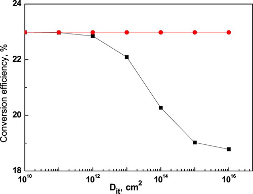
As lattice mismatch of ZnTe (a = 6.1037 Å) with silicon is around 12%, a total defect density Dit of 1013 cm−2 was assumed at the interface between the two materials. To anticipate performance losses with the new designed n+/p − Si/p+− Mo-doped ZnTe solar cell, a 10 nm amorphous Si (a: Si-H) layer was inserted in-between ZnTe:Mo layer and Si base material. Due to very similar Eg (1.72 eV) and χ (3.80 eV) with corresponding ZnTe:Mo material parameters, no hindering barrier for carriers will occur and the amorphous layer provides a positive contribution through its well-established passivation property [Citation32]. With these settings, the open circuit voltage increase improved the PCE to 22.98%. The interface quality can be characterized by recombination velocity or defect density Dit; by varying this parameter from 1010 and 1016 cm−2, Figure shows the high sensitivity of the ZnTe:Mo/Si interface to Dit when the a-Si:H layer is not included. This passivating layer not only allows the conversion efficiency to be stably improved, it enables also the use without any convergence failure a ZnTe layer with higher bandgap (i.e. no Mo-doping). This interesting feature of the thin amorphous layer avoids the additional constraint of the ZnTe doping while dedicating this candidate material only to receiving the oxygen defect specific here to IPV effect.
Figure 4. Influence of ZnTe:Mo/Si interface trap density on solar performance, with (![]()
Thereafter, the denotation ZnTe will be understood as undoped material with an interfacial a-Si:H layer.
3.4. Moving IPV effect within the back ZnTe layer
Owing to a strong emission for the oxygen defect in ZnTe, Wang et al. found an enhanced spectral response for energies down to 1.5 eV that reveals a highly radiative transition [Citation33]. Furthermore, S. Khelifi et al. showed that Jsc could be increased by more than 100% with an improvement of approximately 30% in the conversion efficiency compared to the ZnTe homojunction without oxygen [Citation34]. In our model, the substitutional OTe impurity in ZnTe results in a 0.5 eV defect level from the conduction band [Citation35] and the related effective field ratio was calculated according to Equation (6). Considering the density of traps (Nt) and carriers thermal velocity (νth), capture cross sections (σn and σp) were determined to evaluate the carrier lifetimes τn and τp through the following expression [Citation36]:
(7)
(7) As for the n+/p/p+ all silicon cell (presented in Figure ), the IPV effect appears in the n+/p/ZnTe:O heterostructure through the increase of the short-circuit current that results from the enhancement of the spectral response (Figure (a)). Concerning the current–voltage parameters (Figure (b)), each structure exhibits specific vantages, in terms of either current or voltage. The results detailed in Table show the overall superior performance for the structure with ZnTe:O. The comparison of the two types of structures highlights the following two aspects. First, a notably higher short-circuit current for the all Si cell explained by the superior performance of the IPV mechanism when located in the silicon substrate (this can be noted later in Figure (a)); second, a marked increase in FF (+5.3%) associated with the insertion of the ZnTe layer. Combined with the slight increase of Voc (+50 mV), the FF gain compensates advantageously the specific lower value of Jsc and enables the conversion efficiency to reach 27.15%, higher than that of the all-Si based cell with IPV (26.05%). The open-circuit voltage increase can merely be correlated with the larger bandgap of the ZnTe:O layer.
Figure 5. IPV effect in n+/p/p+ and n+/p/ZnTe solar cells; (a) Quantum efficiency and (b) current-voltage characteristics.
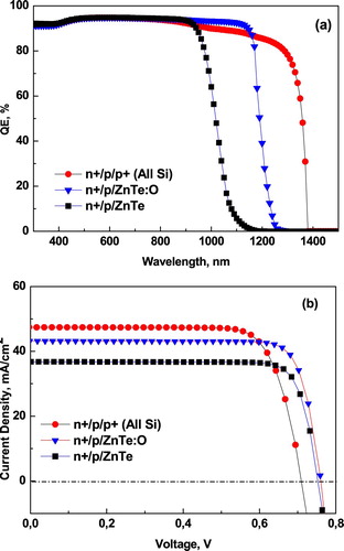
Table 2. Simulation of performance results for silicon based solar cells with different configurations.
In Figure , the capacitance of n+/p/ZnTe:O solar cell is significantly greater than that of all Si n+/p/p+ and shows a peak capacitance shift at higher voltage (ΔV ∼ 45 mV). This performance improvement can be attributed to higher built-in voltage [Citation37]. In the classical theory, the built-in voltage (Vbi) across the solar cell under illumination is usually described as an upper limit to Voc, which depends on the saturation current (J0) given by
(8)
(8) where J00 is the saturation current density prefactor.
Figure 6. Capacitance – voltage characteristics of all silicon (![]()
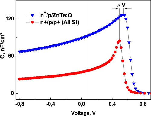
Any increase in Vbi will induce a J0 lowering, which in turn will ultimately lead to an increase of the open circuit voltage (Voc ≈ kT/q. ln [Jsc/J0]).
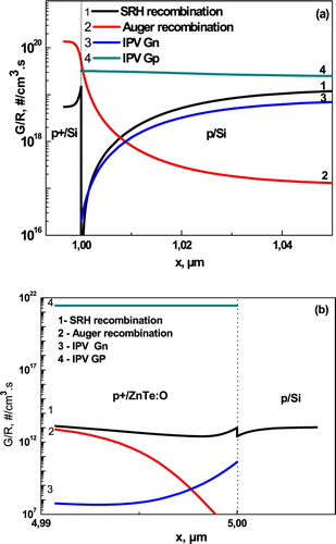
As regard to the short-circuit current, the increase observed for the all-silicon structure can be analysed through the recombination/generation components in the neighbourhood of the back p+/p junction (Figure (a)). On this figure, one can notice in the Si substrate that the optically generation of minority carriers from defect (IPV-Gn) follows very closely the SRH recombination but remains relatively high compared to the Auger recombination. With respect to the structure with ZnTe: O (Figure (b)), optically generation of minority carriers from defect (IPV-Gn) is below both the Auger and the SRH recombination levels. The relatively high doping in the p+/ZnTe:O region explains the preponderance of Auger recombination, but this is necessary to create a back surface field that is able of reducing back recombination and avoiding degradation of the open circuit voltage.
Figure 7. Recombination/generation profiles for IPV structures with (a) p+/Si and (b) p+/ZnTe:O back layer.
Finally, the major contribution of Voc and FF for the heterostructure with ZnTe:O enables advantageously to counterbalance the short circuit current loss and ensure the conversion efficiency improvement.
About the technological feasibility, each material involved in this study has already been the subject of several well-established experimental studies. The main deviations from a conventional structure are the Si/ZnTe:O back junction, the inclusion of the radiative defect and the optical confinement. In particular, highly doped ZnTe with either nitrogen or copper incorporation is a routine operation [Citation38]. On the other hand, the experimental work of S.W. Pak et al. [Citation39] and W. Wang et al. [Citation33] confirmed after oxygen incorporation, an extended spectral response below the band edge relative to undoped ZnTe diodes and showed the intermediate band formation. Nevertheless, the promising results obtained theoretically remain dependent on an almost ideal light trapping at the internal front and back side of the heterostructure. Strategies to implement such systems are being developed but their effectiveness has not yet reached the required levels. We can cite, for instance, novel light trapping structures as reactive ion etched texture (RIE) combined with random pyramid texture (RAN) on silicon and performing excellent light trapping efficiency of 55% [Citation40] and also, a design using ZnTe with a backside distributed Bragg reflector [Citation41] that showed a noticeable improvement in the solar efficiency. The actual adaptation of these systems for getting very high conversion efficiency still needs substantial progress.
4. Conclusion
N+/p/p+ silicon-based solar cell with Si and ZnTe as p+ back-surface field has been explored by numerical simulation using SCAPS 1D-simulator based on accurate physical parameters taken from real experiments. Without IPV effect and owing to larger bandgap value and low back transmittance (reflector property), the structure with ZnTe shows similar performance compared with its analogous “all silicon” structure. A thin passivating layer of amorphous silicon inserted in-between the silicon base and the ZnTe layer allowed for this latter the use of a higher bandgap, along with a significant lower sensitivity to the defects at the interface. IPV effect in the silicon substrate has been checked successfully with an impurity trap positioned at 0.225 eV below the bottom of the conducting band and a gain of 3.4% absolute in PCE was achieved. Adapting the Lucovsky's model, the idea to move the IPV mechanism (represented by an oxygen defect with high radiative transition) from silicon to a thin back ZnTe layer was conclusive. As a result, the conversion efficiency raised up to 27.15% owing to a higher fill factor and (in a lesser extent) to an improved open circuit voltage. Our computational findings on a ZnTe:O back layer as a host material for IPV effect provided relevant physical insight and confirmed great potential to reach higher conversion efficiency. This first step through device simulation can pave the way to assist further technological processing of an advanced heterojunction silicon-based solar cells. To achieve an experimentally forefront efficiency comparable or better to that of present best cells (∼26%), very high light trapping at both sides of the device is a pending issue.
Acknowledgements
Authors are very grateful to Pr. Burgelman (University of Gent, Belgium) for providing SCAPS code.
Disclosure statement
No potential conflict of interest was reported by the authors.
ORCID
M. Boumaour http://orcid.org/0000-0001-7093-2936
S. Sali http://orcid.org/0000-0001-8397-9901
S. Kermadi http://orcid.org/0000-0003-0243-1093
L. Zougar http://orcid.org/0000-0003-3721-5286
A. Bahfir http://orcid.org/0000-0003-3311-2466
Z. Chaieb http://orcid.org/0000-0003-1560-4854
Correction Statement
This article has been republished with minor changes. These changes do not impact the academic content of the article.
References
- Yoshikawa K, Yoshida W, Irie T, et al. Exceeding conversion efficiency of 26% by heterojunction interdigitated back contact solar cell with thin film Si technology. Sol Energy Mater Sol Cells. 2017;173:37–42. doi:10.1016/j.solmat.2017.06.024
- Oxford PV press release, Oxford PV sets world record for perovskite solar cell, 2018; https://www.oxfordpv.com/news/oxfordpv-sets-world-record-perovskite-solar-cell.
- Keevers MJ, Green MA. Efficiency improvements of silicon solar cells by the impurity photovoltaic effect. J Appl Phys. 1994;75:4022. doi: 10.1063/1.356025
- Khelifi S, Verschraegen J, Burgelman M, et al. Numerical simulation of the impurity photovoltaic effect in silicon solar cells. Renew. Energ. 2008;33:293–298. doi: 10.1016/j.renene.2007.05.027
- Breitenstein O. Understanding the current-voltage characteristics of industrial crystalline silicon solar cells by considering inhomogeneous current distributions. Opto Electron Rev. 2013;21(3):259–282. doi: 10.2478/s11772-013-0095-5
- Sahoo HS, Yadav AK, Ray A. Simulation of IPV effect in In-doped c-Si with optimized indium concentration and layer thickness. Phys B. 2011;406:4221–4226. doi: 10.1016/j.physb.2011.07.064
- Yuan J, Shen H, Zhong F, et al. Impurity photovoltaic effect in silicon solar cells doped with tellurium. J Optoelectron Adv Mater Rapid Commun. 2011;5(8):866–869.
- Sircar R, Gupta S, Srivastava DP, et al. Study of Impurity Photovoltaic Effect with Different Doping Materials using SCAPS Simulator. Int J Sci Res Pub. 2013;3(7):1–5. ISSN 2250-3153.
- Macdonald D, McLean K, Deenapanray PNK, et al. Electronically-coupled up-conversion: an alternative approach to impurity photovoltaics in crystalline silicon. Semicond Sci Technol. 2008;23(015001), doi:10.1088/0268-1242/23/1/015001.
- Matin MA, Aliyu MM, Quadery AH, et al. Prospects of novel front and back contacts for high efficiency cadmium telluride thin film solar cells from numerical analysis. Sol Energy Mat Sol Cells. 2010;94:1496–1500. doi: 10.1016/j.solmat.2010.02.042
- Jeetendra S, Naveen CS, Raghu P, et al. Optimization of Thickness of ZnTe Thin Film as Back Contact for CdTe Thin Film Solar Cells. IJERT. 2014;3(5):431–435. ISSN: 2278-0181.
- Zhang L, Liu C, Yang Q, et al. Growth and characterization of highly nitrogen doped ZnTe films on GaAs (001) by molecular beam epitaxy. Mater Sci Semicond Process. 2014;29:351–356. doi: 10.1016/j.mssp.2014.06.045
- Shahriar M, Khan P, Farzana E. Performance Analysis of Impurity Photovoltaic Effect in Solar Cells . IJAPM. 2013;3(1):63–65.
- Beaucarne G, Brown AS, Keevers MJ, et al. The impurity photovoltaic (IPV) effect in wide-bandgap semiconductors: an opportunity for very-high-efficiency solar cells?. Prog Photovolt Res Appl. 2002;10(5):345–353. doi: 10.1002/pip.433
- Lucovsky G. On the photoionization of deep impurity centers in semiconductors. Solid State Commun. 1965;3:299–302. doi: 10.1016/0038-1098(65)90039-6
- Burgelman M, Nollet P, Degrave S. Modelling polycrystalline semiconductor solar cells. Thin Solid Films. 2000;361–362:527–532. doi: 10.1016/S0040-6090(99)00825-1
- Froitzheim A, Stangl R, Elstner L, et al. Proceedings of the 3rd World Conference on Photovoltaic Energy Conversion, Osaka, Japan. p. 279–282.
- Zhu H, Kalkan AK, Hou J, et al. Applications of AMPS-1D for solar cell simulation. AIP Conf Proc. 1999;462:309–314. doi: 10.1063/1.57978
- ATLAS User’s Manual: Device Simulation Software. Silvaco International, Santa Clara (2015).
- Martí A, Cuadra L, López N, et al. Intermediate band solar cells: comparison with shockley-read-hall recombination. Semiconductors. 2004;38(8):946–949. doi: 10.1134/1.1787117
- Sato K, Adachi S. Optical properties of ZnTe. J Appl Phys. 1993;73:926. doi: 10.1063/1.353305
- Güttler G, Queisser HA. Impurity photovoltaic effect in silicon. Energ Convers. 1970;10:51–55. doi: 10.1016/0013-7480(70)90068-9
- Dexter DL. Solid state physics, Vol. 6. New York: Academic Press; 1958; p. 363.
- Sarkar CK. Technology computer aided design: simulation for VLSI MOSFETTaylor & Francis Group; 2013; ISBN: 1351823655, 9781351823654.
- Deng W, Ye F, Xiong Z, et al. Development of high-efficiency industrial p-type Multi-crystalline PERC solar cells with efficiency greater than 21%. Energy Procedia. 2016;92:721–729. doi: 10.1016/j.egypro.2016.07.050
- Azzouzi G, Chegaar M. Impurity photovoltaic effect in silicon solar cell doped with sulphur: a numerical simulation. Phys B. 2011;406:1773–1777. doi: 10.1016/j.physb.2011.02.025
- Schmeits M, Mani AA. Impurity photovoltaic effect inc-Si solar cells. A numerical study. J Appl Phys. 1999;85:2207–2212. doi: 10.1063/1.369528
- Zaari H, Boujnah M, El-Agdal A, et al. Optical properties of ZnTe doped with transition metals (Ti, Cr and Mn). Opt Quant Electron. 2014;46:75–86. doi: 10.1007/s11082-013-9708-y
- Jeetendra S, Nagabhushana H, Mrudula K, et al. Concentration Dependent Optical and Structural Properties of Mo doped ZnTe Thin Films Prepared by e-beam Evaporation Method. Int J Electrochem Sci. 2014;9(6):2944–2954.
- Kiran MSRN, Kshirsagar S, Krishna MG, et al. Structural, optical and nanomechanical properties of (1 1 1) oriented nanocrystalline ZnTe thin films. Eur Phys J Appl Phys. 2010;51:10502. doi: 10.1051/epjap/2010071
- Pettersson J, Platzer-Björkman C, Zimmermann U, et al. Baseline model of graded-absorber Cu(In,Ga)Se2 solar cells applied to cells with Zn1−xMgxO buffer layers. Thin Solid Films. 2011;519:7476–7480. doi: 10.1016/j.tsf.2010.12.141
- Ge J, Ling ZP, Wong J, et al. Optimisation of intrinsic a-Si:H passivation layers in crystalline-amorphous Silicon heterojunction solar cells. Energy Procedia. 2012;15:107–117. doi: 10.1016/j.egypro.2012.02.013
- Wang W, Lin AS, Phillips JD. Intermediate-band photovoltaic solar cell based on ZnTe:O. Appl Phys Lett. 2009;95:011103. doi: 10.1063/1.3166863
- Khelifi S, Mazari H, Belghachi A, et al. Analysis of intermediate band photovoltaic solar cell based on ZnTe:O. J Nanoelectron Optoelectron. 2015;10:333–337. doi: 10.1166/jno.2015.1770
- Wang W, Bowen W, Spanninga S, et al. Optical characteristics of ZnTeO thin films Synthesized by Pulsed Laser Deposition and Molecular Beam Epitaxy. J Electron Mat. 2009;38(1). doi: 10.1007/s11664-008-0577-2
- Montelius L, Grimmeiss HG. The electron capture cross section of Se+in silicon. Semicond Sci Technol. 1988;3:847–852. doi: 10.1088/0268-1242/3/9/004
- Eck M, Van Pham C, Züfle S, et al. Improved efficiency of bulk heterojunction hybrid solar cells by utilizing CdSe quantum dot–graphene nanocomposites. Phys Chem Chem Phys. 2014;16:12251. doi: 10.1039/C4CP01566E
- Abazari M, Ahmad FR, Raghavan C, et al. Carrier density in p-type ZnTe with nitrogen and copper doping. Mater Res Soc Symp Proc. 2013;1538:383–389. doi: 10.1557/opl.2013.1010
- Pak SW, Lee DU, Kim EK. Oxygen incorporation in ZnTe thin films grown by plasma-assisted pulsed laser deposition. Curr Appl Phys. 2014;14:S49–S52. doi: 10.1016/j.cap.2013.11.043
- Barugkin C, Allen T, Chong TK, et al. Light trapping efficiency comparison of Si solar cell textures using spectral photoluminescence. Opt Soc Am. 2015;23(7):A391. doi:10.1364/oe.23.00a391
- Khosroabadi SHK. Design of a high efficiency ultrathin CdS/CdTe solar cell using back surface field and backside distributed Bragg reflector. Opt Soc Am. 2014;22(S3):A921. doi:10.1364/OE.22.00A921