
 ?Mathematical formulae have been encoded as MathML and are displayed in this HTML version using MathJax in order to improve their display. Uncheck the box to turn MathJax off. This feature requires Javascript. Click on a formula to zoom.
Abstract
A novel route of a single flash thermal evaporation technique has been used for deposition of Cu(In,Ga)Se2. This route allows the deposition of stoichiometric CIGS layers direct from powder elements without selenization or any treatment. Structure, optical properties and surface morphology of the deposited films at various substrate temperatures have been investigated using X-ray diffraction (XRD) analysis, Raman spectroscopy, photospectroscopy, Scanning electron microscopy (SEM) and Atomic force microscopy. The structure and the optical properties of deposited films depend on the substrate temperatures which play crucial rule on the stoichiometry of the film by changing mainly the content of selenium. Increasing the substrate temperature improved the crystallinity of the films and the best stoichiometric film has been found at 220°C, the grain size increased from 146 to 286 Å, Whereas, the band gap reduced to 1.37 eV.
1. Introduction
CuInxGa1-xSe2 (CIGS) films have been considered as promising absorber material in thin-film solar cells [Citation1]. CIGS films have been fabricated by several techniques such as; sequential vacuum evaporation [Citation2], sputtering [Citation3], flash-evaporation [Citation4], molecular beam epitaxy [Citation5], hot-wall epitaxy [Citation6], electrodeposition [Citation7], spray pyrolysis [Citation8], chemical ion exchange [Citation9], co-evaporation [Citation10], solvothermal synthesis and spin-coating [Citation11] and nanoparticle-ink fabrication [Citation12]. The CIGS solar cell efficiency of 23.35% [Citation13] set a world record as the highest of any thin-film technology. The most efficient CIGS solar cells have been prepared by co-evaporation, which is a complex processing technique and requires accurate control of all evaporation sources. The flash evaporation technique is one of the simplest method has been used for the deposition of CIGS films. But this technique has some deposition problems such as poor reproducibility, and spitting of material from the evaporation sources [Citation14].
In the present work, we propose a novel single-stage route for growing CIGS films direct from powder. CIGS thin films were deposited by a single nearly cylinder evaporation boat blocked by aluminium oxide ball at the beginning of heating to prevents spitting of materials during the rapid temperatures and to allows the elements to mix with each other before they evaporate in same time from the hole of the boat. Then the capability of using such method to coating stoichiometric CIGS thin film has been investigation by study the Structure, optical properties and surface morphology of the deposited films at various substrate temperatures.
2. Experimental procedure
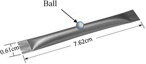
Elements of Cu, In, Ga and Se (99.999%) were weighted; 0.022, 0.02, 0.005 and 0.4 g, respectively, and placed into a directional boat (S17B-.010Ta, Testbourne Ltd). Then the hole of the boat was blocked by a high purity aluminium oxide (Al2O3) ball of 3 mm diameter as shown in Figure . The system was pumped to a base pressure of less than 5 × 10⁻⁵ mbar by turbomolecular pump. The temperature of the boat was increased rapidly to the maximum temperature which the boat can reach (1600°C, Testbourne Ltd). The films were deposited onto standard soda-lime microscope- slide glass at different substrate temperatures, Tg, 100°C, 220°C, 300°C, and 400°C.
Figure 1. Picture of the directional boat blocked by an aluminium oxide ball.
The structure of the CIGS thin films was examined using a Shimadzu XRD-6000 X-ray diffractometer using CuKα radiation (λ = 1.5418 Å). The X-ray tube voltage and current were 40 kV and 30 mA, respectively. Scanning electron microscopy (SEM) and energy-dispersive X-ray (EDX) analysis were performed using a field-emission scanning electron microscope (Quanta FEG250) and a desktop scanning electron microscope (JCM-6000). The transmittance, T(λ), and reflectance, R(λ), spectra of the deposited films were measured at a normal incidence and at an incident angle of 5°. These measurements were conducted in air and at room temperature in the spectral range of 190–2500 nm using a computer-aided double-beam spectrophotometer (Shimadzu 3150 UV–VIS–NIR) with a resolution of 0.1 nm. The deposited film surface morphology was examined using atomic force microscopy (AFM; Veeco CP-II) in non-contact mode with Si tips at a scan rate of 1 Hz. A Bruker Senterra Raman microscope spectrometer equipped with 532 nm (2 mW) excitation laser was used to collect the spectra from the samples at room temperature in the spectral range of 60–1554 cm−1 with the resolution of 3.5 cm−1.
3. Results and discussion
Qualitative and quantitative calculations were performed for the deposited thin films by EDX measurements as shown in Figures and and Table . The composition in the films varies with the substrate temperature dramatically. Se content in the film plays the key rule because it decreases as the substrate temperature increased from 100°C to 220°C. It is clear that there is re-evaporation of unbound Se from the growing film. As a consequence of that, another element’s content increased mainly Cu to give stoichiometric films which deposited between 220°C and 300°C. Then increasing of Cu for Tg > 300°C can be explained by a slight re-evaporation of both In and Ga from the film due to higher temperatures.
Figure 2. The EDX pattern of thin films deposited at different substrate temperatures of 100°C, 200°C, 220°C, 300°C and 400°C.
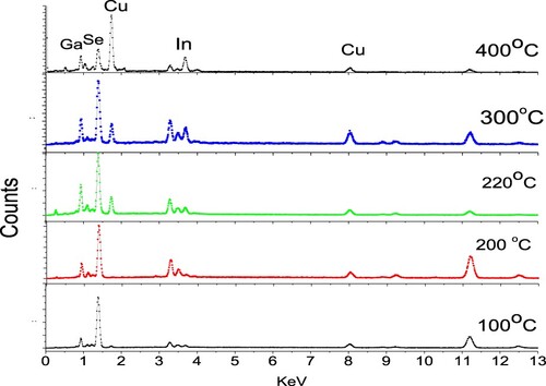
Figure 3. Variation of thin films composition with substrate temperature of 100°C, 200°C, 220°C, 300°C and 400°C.
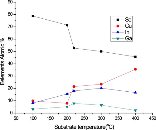
Table 1. The elemental composition analysed from the EDX spectra obtained for thin films with substrate temperature of 100°C, 200°C, 220°C, 300°C and 400°C.
The stoichiometric films which were deposited between 220°C and 300°C are almost fully oriented along < 112 > as shown in Figure . This was verified by ICDD (International Centre for Diffraction Data) database with card number 00-035-1101. Then, at higher temperature, 400°C, another orientations exist < 204 > and < 220 > with increasing Cu in expense of Se. The grain size, D, of the crystallites was calculated using Sherrer’s formula [Citation15]:
(1)
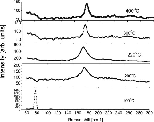
(1) where λ is the wavelength of the X-ray, θ is the diffracted angle, and β is the full width at half-maximum of the respective peak in radians. The grain size, D, increased from around 146 to 286 Å for the thin film deposited at 100°C and 400°C, respectively. The increase in grain size is due to the improvement in crystallinity [Citation16]. As shown from Figure , the increasing of grain size nearly linearly with substrate, with slope ∼0.48 Å/°C, despite variation of film’s stoichiometry. Figure depicts Raman spectra measured at room temperature. The film which was deposited at 100°C gave a high intensity peak at 77 cm−1 which could be assigned to the B1 mode [Citation17]. Whereas another films which were deposited at 200°C, 220°C, 300°C and 400°C had peaks at 172, 169.8, 173 and 173, respectively. These peaks were assigned to the A1 mode [Citation18], which is the strongest mode generally observed in the Raman spectra of I-III-VI2 chalcopyrite compounds. The highest frequency of A1 mode is observed at 220°C with the highest Ga content in CIGS films [Citation17] and the films became more stoichiometry chalcopyrite compounds. Whereas the intensity of the films which were deposited at higher than 220°C reduced and FWHM increased indicated that decreasing the stoichiometry of the film. These facts confirmed by increasing the copper contents.
Figure 4. X-ray diffraction patterns of deposited thin films at different substrate temperatures of 100°C, 200°C, 220°C, 300°C and 400°C.
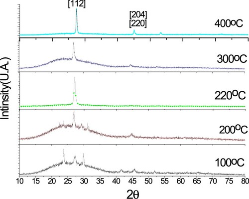
Figure 5. Variation of thin film grain sizes with the substrate temperature of 100°C, 200°C, 300°C and 400°C.
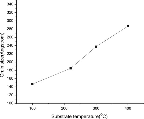
Figure 6. Raman spectra of the thin films deposited at different substrate temperatures of 100°C, 200°C, 220°C, 300°C and 400°C.
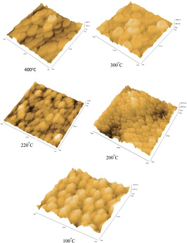
The images of SEM of thin films are shown in Figure revealed no cracking on the samples surface and good adhesive films, demonstrating that the evaporation of CIGS elements by this technique is feasible for fabricating good CIGS absorption layers. From these images, it is clear that substrate temperatures significantly influenced the surface morphology. Figure shows the AFM images of the films and the Root-Mean-Square roughness have been deduced. It has been found that the roughness of non-stoichiometric films, which were deposited at low and high substrate temperatures (100°C and 400°C), are small around 25 nm, whereas the films which were deposited between 200°C and 300°C have higher roughness between 63 and 74 nm.
Figure 7. SEM micrographs of CIGS thin films deposited at different substrate temperatures of 100°C, 200°C, 220°C, 300°C and 400°C.
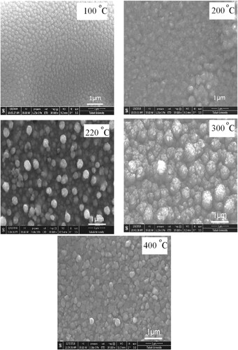
Figure 8. AFM images of the thin films at various substrate temperatures of 100°C, 200°C, 220°C, 300°C and 400°C.
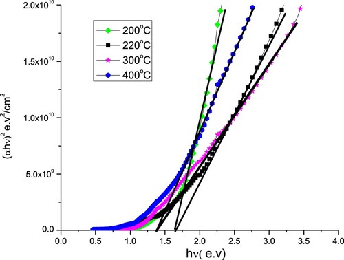
The band gapes of samples which were deposited at 200°C and 220°C are nearly the same around 1.64 eV whereas the samples deposited at 300°C and 400°C have smaller band gaps 1.37 eV as deduced from Figure . The decrease in the band gap with increasing substrate temperature can likely to be attributed to an increase of the particle size and a decrease in the strain in films [Citation19] and could be to the reduction of Ga content [Citation20,Citation21].
Figure 9. Plots of (αhν)2 versus hν for thin films deposited at various substrate temperatures of 200°C, 220°C, 300°C and 400°C.
4. Conclusion
Stoichiometric CIGS layers have been fabricated directly from powder elements without selenization or any treatment by flash thermal evaporation technique using a directional boat. The substrate temperature plays a key role on the composition of films. Selenium content decreased as the substrate temperature increased which changed the stoichiometry of the film dramatically. The film nearly maintain its composition for substrate temperature between 220°C and 300°C after that the copper content increased while the rest of elements decreased. The grain size increased nearly double as the substrate temperature increased from at 100°C and 400°C, whereas the band gape decreased.
Disclosure statement
No potential conflict of interest was reported by the authors.
References
- Baji Z, Lábadi Z, Molnár G, et al. Post-selenization of stacked precursor layers for CIGS. Vacuum. 2013;92:44–51. doi: 10.1016/j.vacuum.2012.11.012
- Deepa K, Jayakrishnan R, Vijayakumar KP, et al. Sub-micrometer thick CuInSe2 films for solar cells using sequential elemental evaporation. Sol Energy. 2009;83(7):964–968. doi: 10.1016/j.solener.2009.01.016
- Piekoszewski J, Loferski J, Beaulieu R, et al. RF-sputtered CuInSe2 thin films. Sol Energy Mater. 1980;2(3):363–372. doi: 10.1016/0165-1633(80)90012-X
- Akl A, Ashour A, Ramadan A, et al. Structural study of flash evaporated CuInSe2 thin films. Vacuum. 2001;61(1):75–84. doi: 10.1016/S0042-207X(00)00458-9
- White F, Clark AH, Graf MC, et al. Growth of CuInSe2 films using molecular beam epitaxy. J Vac Sci Technol. 1979;16(2):287–289. doi: 10.1116/1.569928
- Agilan S, Mangalaraj D, Narayandass SK, et al. Structure and temperature dependence of conduction mechanisms in hot wall deposited CuInSe2 thin films and effect of back contact layer in CuInSe2 based solar cells. Vacuum. 2010;84(10):1220–1225. doi: 10.1016/j.vacuum.2009.10.029
- Kang S, Kim Y, Choi D, et al. Characterization of electrodeposited CuInSe2 (CIS) film. Electrochim Acta. 2006;51(21):4433–4438. doi: 10.1016/j.electacta.2005.12.021
- Nguyen D, Takehara K, Ryo T, et al. Back contact materials for superstrate CuInS2 solar cells. Energy Procedia. 2011;10:49–54. doi: 10.1016/j.egypro.2011.10.151
- Joshi R A, Taur V S, Ghule A V, et al. Stoichiometry controlled conversion efficiency in nanostructured heterojunction solar cell of CdS/CuInSXSe2−X grown by chemical ion exchange method at room temperature. Sol Energy. 2011;85(7):1316–1321. doi: 10.1016/j.solener.2011.03.013
- Jung S, Ahn S, Ho Yun J, et al. Effects of Ga contents on properties of CIGS thin films and solar cells fabricated by co-evaporation technique. Curr Appl Phys. 2010;10(4):990–996. doi: 10.1016/j.cap.2009.11.082
- Liu Y, Kong D, Li J, et al. Preparation of Cu(In,Ga)Se2 thin film by solvothermal and spin-coating process. J Energy Procedia. 2012;16(A):217–222. doi: 10.1016/j.egypro.2012.01.036
- Liu CP, Chuang CL. Fabrication of CIGS nanoparticle-ink using ball milling technology for applied in CIGS thin films solar cell. Powder Technol. 2012;229:78–83. doi: 10.1016/j.powtec.2012.06.011
- Green M, Dunlop E, Levi D, et al. Solar cell efficiency tables (version 54). Prog Photovolt. 2019;27(7):565–575. doi: 10.1002/pip.3171
- Klenk M, Schenker O, Alberts V, et al. Preparation of device quality chalcopyrite thin films by thermal evaporation of compound materials. Semicond Sci Technol. 2002;17(5):435–439. doi: 10.1088/0268-1242/17/5/305
- Maissel LI, Glang R. Hand book of thin film technology. New York (NY): McGraw-Hill; 1980.
- Yılmaz K, Karaagac H. Annealing effects on structural, optical and electrical properties of e-beam evaporated CuIn0.5Ga0.5Te2 thin films. Appl Surf Sci. 2010;256(21):6454–6458. doi: 10.1016/j.apsusc.2010.04.034
- Roy S, Guha P, Kundu SN, et al. Preparation of device quality chalcopyrite thin films by thermal evaporation of compound materials. Mater Chem Phys. 2002;73(1):24–30. doi: 10.1016/S0254-0584(01)00345-5
- Witte W, Kniese R, Powalla M. Raman investigations of Cu(InGa)Se2 thin films with various copper contents. Thin Solid Films. 2008;517(2):867–869. doi: 10.1016/j.tsf.2008.07.011
- Prabahar S, Balasubramanian V, Suryanarayanan N, et al. Optical properties of copper indium diselenide thin films. Chalcogenide Lett. 2010;7(1):49–58.
- Aissat A, Fathi M, Vilcot JP. Development and simulation of a structure based on CuIn1-xGaxSe2 semiconductors alloys for a new generation of photovoltaic cells. Energy Procedia. 2012;18:197–204. doi: 10.1016/j.egypro.2012.05.031
- Zhao-Hui L, Cho ES, Kwon SJ. Properties of the Cu(In,Ga)Se2 absorbers deposited by electron-beam evaporation method for solar cells. Curr Appl Phys. 2011;11(1):28–33. doi: 10.1016/j.cap.2010.06.013