
 ?Mathematical formulae have been encoded as MathML and are displayed in this HTML version using MathJax in order to improve their display. Uncheck the box to turn MathJax off. This feature requires Javascript. Click on a formula to zoom.
Abstract
Transparent semiconductor low cost thin films from benign, earth-abundant materials have been reported. Copper acetate, zinc acetate, stannous chloride, and thiourea have been used as precursors for the preparation of the parent thin film, with dimethyl sulfoxide as the solvent. Both diethanol amine and ethylene glycol have been used as modifiers. Transmittance, reflectance, and absorption coefficient from 190 to 2500 nm for these films have been presented. The linear refractive index n and the absorption index k have been evaluated. Current–voltage curves for the films have been presented. The bandgap for these thin films has been evaluated. From transmittance and the current–voltage measurements, the figure of merit has been calculated. The reported data show that these films are good candidate as electrodes in optoelectronic devices.
Highlights
Impact of diethanol amine (DEA) and ethylene glycol (EG) as additives for precursors of Cu-Zn-Sn-S nano composite thin films has been reported and characterized
These additives change the pH of the precursor solutions and yield changes in optical and electrical properties
SEM images show that the films have particle like structure with nanometer scale, and XRD characteristics show that the films are amorphous
While DEA decreases the peak reflectance of the pristine film, EG increases it
DEA increases the current flow compared to pristine films
1. Introduction
The quaternary materials of Cu-Zn-Sn-S (CZTS) for composites are of practical interest. These materials are abundant in nature, benign, and not expensive. These composites are used in a variety of applications such as lithium battery and solar cell absorbing medium and molecular hydrogen production [Citation1]. One of these composites that are widely used is Cu2ZnSnS4. The stable phase of this composite is kestrite, which has a tetragonal structure, with bandgap of 1.45–1.6 Ev [Citation2,Citation3], which is theoretically optimum for solar cell absorbers.
Different methods have been used to manufacture CZTS composite thin films like spray pyrolysis [Citation4] non-vacuum liquid method such as sol–gel spin coating [Citation5–7] and sol–gel dip coating [Citation8,Citation9].
The sol–gel spin coating method shows advantages such as simple and not expensive method for the CZTS composite. CZTS films have great technological importance as an absorber in solar cell devices. For example, Pandey et al. [Citation10] and Guo et al. [Citation11] utilized these films in solar cell applications. Also, Tumbul et al. utilized CZTS as low cost thin film absorber [Citation12]. Gadallah et al. investigated the effect of Al doping on the properties of CZTS thin films prepared by sol–gel spin coating [Citation13]. According to their work at certain concentration of Al there is optimum in the structural and optical properties for the films. Atwee et al. investigated the effect of film thickness on the properties of CZTS [Citation14]. At certain thickness, there is an enhancement of structural and optical properties. Abd El-Gawad et al. investigated the influence of preparation condition on the properties of Cu-Zn-S (CZS) thin films [Citation15]. At certain number of layers and temperature the structural and optical properties are enhanced. Khalil et al. investigated the effect of Ag doping on the properties of CZS thin films [Citation16]. At certain concentrations of Ag, the films were homogeneous and more crystalline. Also, the effect of substrate was investigated for enhancing the structural properties. Other applications for nano materials are photocatalysis [Citation17] and transparent conductive layers [Citation18,Citation19]. For example, Goktas and Goktas reported on the recent progress of ZnO photocatalysts. Bikash Sarma et al. demonstrated transparent conductive Al-doped ZnO thin films by DC magnetron sputtering with crystallite size in the range 16–21 nm and the figure of merit was about 1.99 × 10⁻²/Ω. Chavez-Vargas et al. prepared transparent conductive F-doped ZnO thin films by the chemical spray technique with maximum figure of merit of 7.57 × 10⁻³/Ω. GaeHun Jo and Jung-Hyuk Koh investigate the effect of laser annealing on Ga-doped ZnO for transparent conductive thin films. They achieved a figure of merit of 2.5 × 10⁻⁵/Ω. According to a work published by Fang-Hsing Wang and his co-workers, a transparent conductive Ti and H doped ZnO thin films were prepared by radio frequency magnetron sputtering. The highest figure of merit they achieved was 4.74 × 10⁻³/Ω.
Nanomaterial thin films are strongly affected by the pH. Afşin Kariper and co-workers reported on the effect of pH on structural optical and electrical properties of some chalcogenide thin films such as CdS [Citation20], ZnSe [Citation21], CdSe [Citation22], PbSe [Citation23], Sb2S3 [Citation24], MnSe [Citation25], CrSe [Citation26], BiSe [Citation27], CrSe [Citation28], MnTe [Citation29], CuS [Citation30], and ZnS [Citation31]. In addition, the nanomaterials are also affected by complexing agents [Citation32]. Compared to these chalcogenide composites, CZTS materials are abundant, benign, and not expensive materials.
Here the effect of diethanolamine and ethylene glycol as additives with the precursors of CZTS materials on the properties of CZTS thin films has been investigated. XRD characteristics, SEM images, transmittance, reflectance, extinction coefficient, refractive index and DC current–voltage results have been reported. Reasons for changing the properties have been reported.
2. Experimental details
2.1. Materials and equipment/devices used
The precursors used in manufacturing the thin films are copper acetate Cu(CH3COO)2, zinc acetate dehydrate ((CH3COO)2 Zn·2H2O), stannous chloride (SnCl2), and thiourea (CH4N2S) as sources for copper, zinc, tin, and sulfur, with a molar ratio of 1:0.5:0.5:4, respectively. The molar ratios and the weight ratios of Cu:Zn:Sn:S are shown in Table . Thiourea has the highest molar ratio.
Table 1. Weight and molar percentage of the chemicals used.
The additives used as modifiers are diethanolamine (NH(CH2CH2OH)2) and ethylene glycol. The solvent used is dimethylsulfoxide (C2H6OS). For cleaning the glass substrates, acetone and 2 propanol have been used.
The model of the spin coater used is KW-4A with a maximum spin speed of 8000 round per minute (rpm). For transmittance and reflectance measurements, a Shmaziu 3150 double beam spectrophotometer has been used for Ultra violet, visible, and near infrared regions. For x-ray diffraction measurements, a Shimadzu XRD-6000 X-ray diffractometer has been used with a wavelength of 1.564. The voltage applied between electrodes of the x-ray tube is 40 kV and the current is mA. For the current–voltage curve, a DC power supply, model Extech 382213 with voltage and current display has been used.
2.2. Sample preparation
The copper acetate, zinc acetate, stannous chloride, and thiourea are dissolved in 50 mL of dimethyl sulfoxide. The molar ratio as well as the weight ratio of these precursors in the solvent are presented in Table . The dissolving process was carried out for 20 min with stirring with a magnet till a clear solution with light yellow solution was obtained. The glass substrates were cleaned using acetone and 2 propanol and then heated for the removal of residual solvents. The precursor solution covered the substrates and spun with a speed of 3000 rpm for one minute. Then they were heated at 310° using a hot plate for 5 min. The process of deposition and heating was repeated 7 times. The films had a light brown colour.
3. Results and discussion
The results of three thin films have been presented in this section. The films were designated as a (pristine film), b (with diethanolamine as additive), and c (with ethylene glycol as additive). Since the pH and viscosity affects the properties of nanomaterials, both of these measurements have been carried out. Table shows the pH as well as the viscosity for the sample a, b, and c.
Table 2. pH and viscosity of samples a, b, and c.
While diethanol amine increases the pH from 7.212 to 7.613, ethylene glycol decreases the pH from 7.212 to 7.012. Also, diethanolamine increases the viscosity from 2.3 to 2.5 mPa s.
For XRD characteristics, the pH of the precursor solution affects the structural properties of CZTS. F. Aslan reported the effect of pH on the structural and optical properties CZTS films [Citation33]. Also, the type of salt affects the crystallinity. For example, Tumbul et al. reported the effect of zinc salt on the structural properties of CZTS [Citation34]. The samples reported here are amorphous. Here the pH is greater than or equal to 7, in contrast to that reported in [Citation33] which has a pH lower than or equal to 5. Figure presents images taken by a scanning electron microscope with magnification of 120,000. The images show that the films are homogeneous with particle-like structure in the nanosize scale. The particle size varies from 16 to 30 nm, based on the additive. The pH value affects the properties of the films as reported [Citation20–30]. Also, the viscosity of the solution precursor affects the properties of the deposited thin films. Table shows the pH and the viscosity of the precursor solutions corresponding to samples a, b, and c. For elemental analysis, energy dispersive x-ray spectroscopy has been used. The weight and molar ratios in precursors of Cu-Zn-Sn-S are mentioned in Table . The ratio of these elements in the films using EDX is shown in Table . When diethanolamine or ethylene glycol was added to the precursors, the molar ratio of the compound is changed. Tables and show the ratio of the elements when diethanolamine and ethylene glycol are added using EDX (Table ).
Figure 1. SEM images of samples a, b, and c.
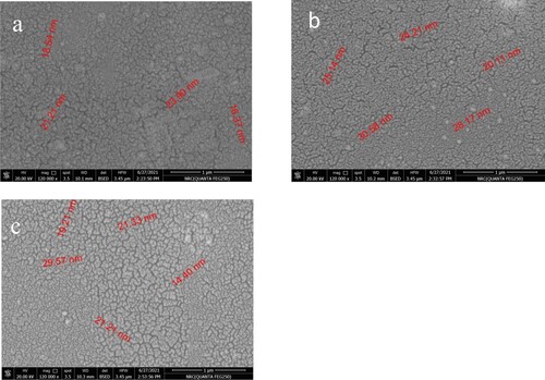
Table 3. Atomic and weight percentage of sample a using EDX measurements.
Table 4. Atomic and weight percentage of sample a using EDX measurements.
Table 5. Atomic and weight percentage of sample a using EDX measurements.
Figure shows the transmittance of these films in the spectral region from 190 nm (ultraviolet) to 2500 nm (end of the near infrared region). In the beginning (from 190 till about 300 nm) the value of transmittance is approximately zero, which is attributed to light absorption in this region, hence this region can be called a strong absorption region. Then, with increasing wavelength, the transmittance increases sharply till it reaches a maximum value then it approximately becomes constant. At constant transmittance, the films are transparent that is to say T + R ∼ 1. The film that has the maximum transmittance is film b with a maximum transmittance of ∼0.78 at 678 nm. Note that all films approximately have the same transmittance from 190 till 335 nm, then film b has higher transmittance from 336 till 878 nm compared to the other films. Then from 976 till 2500 nm, film c has higher transmittance compared to films a and b. Hence, the additives increase the film transmittance in certain spectral regions. The maximum transmittance of film c is about 0.735 and that of a is about 0.70.
Figure 2. Spectroscopic transmittance of samples a, b, and c.
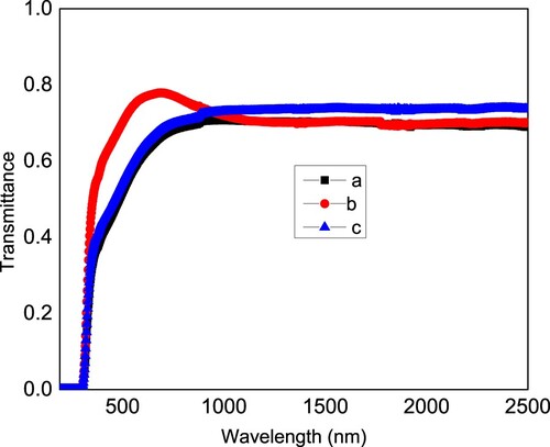
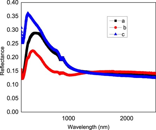
Figure presents the reflectance of the films in the spectral region from 190 to 2500 nm. All films show a peak in the reflectance curve, however the peak position and the peak amplitude vary from a to b to c. While film a shows a peak at 428 nm with a value of 0.289, film b shows a peak at 386 nm with a value of 0.224, and film c shows a peak at 302 nm with a reflectance of 0.361. The change of reflectance from sample to another is strongly affected by the particle size, which in turns is affected by the pH of the precursors. This is in agreement with the literature [Citation20–31]. As shown in Figure , the sample a has higher reflectance compared to sample b. And sample c has higher reflectance compared to sample a. Note that sample b has higher pH value compared to sample a and sample a has higher pH value compared to sample c. so here the higher the pH, the lower the reflectance.
Figure 3. Spectroscopic reflectance of samples a, b, and c.
The absorption coefficient is related to reflectance R and transmittance T by the following relation:
where d is the film thickness.
The extinction coefficient k (also known as the absorption index) is related to the absorption coefficient by the following equation:
where λ is the wavelength. The extinction coefficient is presented in Figure (a) as a function of the wavelength. The refractive index is related to the reflectance and extinction coefficients by the following relation:
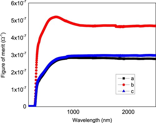
The refractive index of the three films is depicted in Figure (b). Both the peak and amplitude of the refractive index change from a to b to c film. While the addition of ethylene glycol in the precursor solution led to an increase in the amplitude of refractive index peak from 3.287 to 3.871 and shifts the peak position from 422 to 336 nm, the addition of diethanol amine decreases the refractive index from 3.287 to 2.785 and the peak position is shifted from 422 to 390 nm. Hence, the additives modify the refractive index of the films. An important figure for a transparent conductive electrode is the figure of merit. Figure shows the figure of merit of the prepared films. As shown in the figure, the film b has a higher figure of merit value compared to films a and c and film c has a higher value of figure of merit compared to film a. Due to the change of the the reflectance of the films with the additives, the figure of merit changes too. For transparent conductive applications, it is desirable to have high figure of merit. Hence, film b with diethanol amine as a modifier is desirable in transparent conductive applications.
Figure 4. Extinction coefficient k (a) and refractive index versus wavelength (b) for samples a, b, and c.
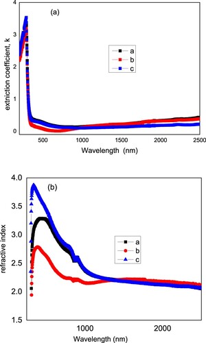
Figure 5. Figure of merit as a function of wavelength for samples a, b, and c.
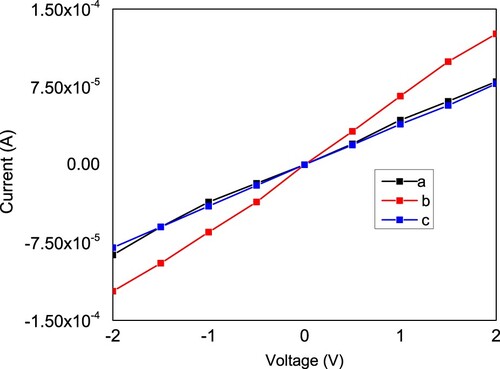
The current–voltage curves for these films are depicted in Figure . From this figure one can obtain the sheet resistance of these films which is the reciprocal of the slope. The values of the sheet resistance of films a, b, and c are 24.45, 15.748 and 25.445 kΩ, respectively. Hence, the addition of diethanol amine during dissolving the precursors improves the electrical properties of the films. Thus, these films can find applications as transparent conductive electrodes in the visible and in the near infrared regions.
Figure 6. Current–voltage curves for samples a, b, and c.
4. Conclusions
Wide bandgap transparent semiconducting thin films have been prepared using nanocomposites of Cu-Zn-Sn-S materials with different compositions. The films are homogeneous continuous with particle like structure in the nano scale. Elemental analysis using energy dispersive x ray analysis has been presented. Spectroscopic measurements for transmittance, reflectance, and refractive index have been reported. The figure of merit for the samples has been calculated. The current–voltage curves for these samples have been demonstrated. The results show that the nano composite materials are promising for the semiconductor industry.
Disclosure statement
No potential conflict of interest was reported by the author(s).
References
- Wang J, Zhang P, Song X, et al. Cu2ZnSnS4 thin films: spin coating synthesis and photoelectrochemistry. RSC Adv. 2014;4:21318–21324.
- Katagiri H, Saitoh K, Washio T, et al. Development of thin film solar cell based on Cu2ZnSnS4 thin films. Sol Energy Mater Sol Cells. 2001;65:141.
- Katagiri H. Cu2ZnSnS4 thin film solar cells. Thin Solid Films. 2005;480–481:426.
- Kumar YBK, Bhaskar PU, SBabu G, et al. Effect of copper salt and thiourea concentrations on the formation of Cu2 ZnSnS4 thin films by spray pyrolysis. Phys Status Solidi A. 2010;207:149–156.
- Jiang M, Li Y, Dhakal R, et al. Cu2ZnSnS4 polycrystalline thin films with large densely packed grains prepared by sol-gel method. J Photonics Energy. 2011;1:019501–1.
- Islam S, Hossain MA, Kabir H, et al. Optical, structural and morphological properties of spin coated. Int J Thin Films Sci Technol. 2015;3:155.
- Swami S, Kumar A, Dutta V. Deposition of kesterite Cu2ZnSnS4 (CZTS) thin films by spin coating technique for solar cell application. Energy Procedia. 2013;33:198–202.
- Chaudhuri TK, Tiwari D. Earth-abundant non-toxic Cu2ZnSnS4 thin films by direct liquid coating from metal–thiourea precursor solution. Solar Energy Mater Solar Cells. 2012;101:46–50.
- Sun Y, Zong K, Zheng H, et al. Ethylene glycol-based dip coating route for the synthesis of Cu2ZnSnS4 thin film. Mater Lett. 2013;92:195–197.
- Pandey K, Mohanty BC. Influencing mechanism of post-sulfurization with sulfur flakes on phase evolution and Schottky diode characteristic of Cu2ZnSnS4 thin films sputter deposited from a single target. Sol Energy. 2021;228:333–338.
- Guo J, Sun S, Liu B, et al. Influence of Na2S treatment on CZTS/Mo interface in Cu2ZnSnS4 solar cells annealed in sulfur-free atmosphere. Optik. 2021;242:166998.
- Tumbul A, Aslan F, Goktas A, et al. Highly stable ethanol-based Cu2ZnSnS4 (CZTS) low-cost thin film absorber: effect of solution aging. Mater Chem Phys. 2021;258:123997.
- Gadallah A-S, Salim MA, Atwee T, et al. Effect of Al doping on structural, morphological, optical, and electrical properties of Cu2ZnSnS4 thin films prepared by sol-gel spin coating. Optik. 2018;159:275–282.
- Atwee T, Gadallah A-S, Salim MA, et al. Effect of film thickness on structural, morphological, and optical properties of Cu2ZnSnS4 thin films prepared by sol–gel spin coating. Appl Phys A. 2019;125:270.
- Abd El-Gawad AHM, Khalil AAI, Gadallah A-S. Influence of preparation conditions on the properties of silver doped copper-zinc sulfide thin films prepared via sol-gel spin coating technique. Optik. 2020;223:165561.
- Khalil AAI, Abd El-Gawad AHM, Gadallah A-S. Impact of silver dopants on structural, morphological, optical, and electrical properties of copper-zinc sulfide thin films prepared via sol-gel spin coating method. Opt Mater. 2020;109:110250.
- Goktas S, Goktas A. A comparative study on recent progress in efficient ZnO based nanocomposite and heterojunction photocatalysts: a review. J Alloys Compd. 2021;863:158734.
- Sarma B, Barman D, Sarma BK. AZO (Al:ZnO) thin films with high figure of merit as stable indium free transparent conducting oxide. Appl Surf Sci. 2019;479:786–795.
- Chavez-Vargas E, Jayaraman VK, Karthik TVK, et al. Effect of doping concentration, solvent proportions and solution aging on the figure of merit of chemically sprayed ZnO:F thin films. J Mater Sci: Mater Electron. 2018;29:15821–15828.
- Kariper İA, Güneri E, Göde F, et al. The structural, electrical and optical properties of CdS thin films as a function of pH. Mater Chem Phys. 2011;129:183–188.
- Tezel FM, Kariper İA. Effect of pH on the structural and optical properties of polycrystalline ZnSe thin films produced by CBD method. Int J Mod Phys B. 2019;33(05):1950024.
- Kariper IA.. Optical and structural properties of CdSe thin film produced by chemical bath deposition. J Non-Oxide Glasses. 2016;8:1–9.
- Kariper IA. Amorphous PBSE thin film produced by chemical bath deposition at pH of 5–8. Surf Rev Lett. 2020;27:1950128.
- Tezel NS, Tezel FM, Kariper İA. Surface and electro-optical properties of amorphous Sb2S3 thin films. Appl Phys A. 2019;125:1–16.
- Kariper İA. A New route to synthesize MnSe thin films by chemical bath deposition method. Mater Res. 2018;21(2):e20170215.
- Fatma Meydaneri T, Kariper İA. A new process to synthesize CrSe thin films with nanosize by CBD method. Mater Res Express. 2018;6:036412.
- Fatma Meydaneri T, Kariper İA. Optical, electrical, structural and magnetic properties of BiSe thin films produced by CBD on different substrates for optoelectronics applications. Mater Res Express. 2018;6:016425.
- Kariper İA. Synthesis and characterization of CrSe thin film produced via chemical bath deposition. Opt Rev. 2017;24:139–146.
- Kariper İA, Göde F. Influence of pH on the structural and optical properties of polycrystalline MnTe2 thin films produced by chemical bath deposition method. Acta Phys Pol A. 2017;132:531.
- Guneri E, Kariper A. Optical properties of amorphous CuS thin films deposited chemically at different pH values. J Alloys Compd. 2012;516:20–26.
- Göde F, Güneri E, Kariper A, et al. Influence of annealing temperature on the structural, optical and electrical properties of amorphous zinc sulfide thin films. J Phys Conf Ser. 2011;326:012020.
- Göde F, KarIper IA, GünerI E, et al. Effect of complexing agent on the structural, optical and electrical properties of polycrystalline indium sulfide thin films deposited by chemical bath deposition. Acta Phys Pol A. 2017;132:527.
- Aslan F, Göktaş A, Tumbul A. Influence of pH on structural, optical and electrical properties of solution processed Cu2ZnSnS4 thin film absorbers. Mater Sci Semicond Process. 2016;43:139–143.
- Tumbul A, Göktaş A, Zarbali MZ, et al.. Structural, morphological and optical properties of the vacuum-free processed CZTS thin film absorbers. Mater Res Express. 2018, in press.