
ABSTRACT
The laser induced forward transfer and sintering of metal nanoparticle inks has been proven a key enabling technology for flexible electronics. Nevertheless, many challenges concerning the conformal processing of non-planar substrates incorporating thermally sensitive layers are yet to be addressed. In this work, we study the behaviour of conformal laser printing of silver nanoparticle inks on patterned samples comprising sensitive underlying structures, by correlating the laser sintering powers employed to the undesired effects on the adjacent interfaces. The latter include demanding surface topographies with periodic patterns and micro-components exhibiting aspect ratio in the nano to 100-micron scale. We investigate the contribution of crucial processing parameters, such as the per pulse energy, repetition rate and the pulse to pulse spatial and temporal overlap to the overall result. The demonstrated results validate the versatility of laser processing which can offer application specific solutions on different use cases involving multilayered and multimaterial electronics.
1. Introduction
The rapid advancement of organic and large area electronics over the past 20 years, has fostered disruptive innovations at the chip and system levels, paving the way for the next generation of flexible and wearable devices and sensors (Lee et al. Citation2017; Hanitra et al. Citation2018; Sun et al. Citation2014). Reports of demonstrations of electronic components and functional flexible devices displaying quality factors comparable to Si electronics have been published (Dang et al. Citation2018). This achievement has been accomplished owing to the introduction of new materials in addition to novel and compatible with the requirements of flexible and multilayered substrates additive manufacturing processes, such as laser based fabrication (Zhou et al. Citation2019). The additive manufacturing technology and more specifically laser printing (Ko et al. Citation2010; Piqu et al. Citation2016) and laser sintering (Ko et al. Citation2007) offer significant advantages over the standard microelectronic fabrication techniques (CMOS processing): they are digital processes omitting the need for masks and multi-step top-down processing involving chemicals and solvents. These techniques are implemented in a direct, single-step procedure, are resilient to ambient conditions and therefore free of the need for controlled atmosphere within a clean room (Kattamis et al. Citation2011).
Furthermore, when it comes to the fabrication of complex functional devices with flexible form factors, the standard clean room processes are characterised by costly, subtractive, time consuming steps which often involve reactant chemicals and toxic solvents. As a consequence, these techniques fail to meet the highly challenging requirements, namely the non-planar morphology and the flexibility of the component design, as well as the sensitive materials comprising the device’s stack of layers. Conversely, printable dispersions constitute a viable solution for the effective processing of multi-layer and multi-material stacks: numerous printable dispersions (inks) have been developed over the last 15 years, involving different material types such as metals, semiconductors, and dielectrics (Manikam and Cheong Citation2011; Suganuma, Kim, and Kim Citation2009). Due to their extraordinary characteristics e.g. small size and large surface to volume ratio facilitating the transition from the liquid to the solid state, these inks are suitable for the manufacturing of printed electronics at low-temperature processing. However, the great challenge of determining the appropriate combination of solvent composition and process parameters impedes the standardisation in ink-based solution processing techniques for multilayered stacks (Bolduc et al. Citation2018). The implementation of advanced additive manufacturing techniques, can unlock the full potential of the aforementioned materials, with a variety of demonstrations of active components already reported, such as transistors (Rother et al. Citation2017; Fukuda and Someya Citation2017), energy storage devices (Giannakou et al. Citation2019) and low cost sensors (Han et al. Citation2019) including carbon nanotube based photodetectors (Zhang et al. Citation2017).
Moreover, regarding the additive manufacturing of interconnections, despite the recent advances (Bolduc et al. Citation2018), especially with the employment of inkjet printing technique, limitations related to printing head clogging issues and the customised inks are still present. Also, several challenges relating to the ink employed need to be addressed, namely the non uniform conductivity across the printed interconnects, the shrinkage of ink after curing procedure and the reliability of the interconnects upon thermal stresses (Kim et al. Citation2017). In order for the additive manufacturing to be fully upscaled to mass production, the throughput of the processes involved still lack in comparison to the conventional manufacturing techniques (Coelho et al. Citation2020).
A particular challenge, which still remains unmet is the processing of fully-patterned non planar substrates incorporating low glass transition temperature (Tg) materials, that involve micro-components with periodicity and aspect ratio in the nano to hundreds micron scale. While essential for devices in a plethora of applications, their fabrication is still hindered by the limitations of the manufacturing techniques currently dominant in the industry, which among other, concern the lack of conformity between the top and the bottom layers of the stack (Wu, Huang, and Chen Citation2017). More specifically, regarding the traditional technique of photo-lithography for the manufacturing of conductive lines that can operate as gate electrodes for an OTFT, limitations occur due to the non-planar nature of the substrate, which consists of a metal-gate dielectric stack and requires materials and process, which can sustain conformal deposition. The existence of these metals create a periodic grid with a height of hundreds of nanometres, which has strong implications on the resolution and eventually make the use of a gap depended lithography mask ineffective (Markey et al. Citation2015).
Regarding the conductive materials, the realisation of flexible electronic components fabricated by laser printing and sintering have been enabled by high quality silver nanoparticle (NP) inks (Zhou et al. Citation2019), widely utilised in printed electronics for conductive structures, with a growing number of articles investigating the improvement of coating and sintering methods (Kumar et al. Citation2019; Morales et al. Citation2018).
Previous reports have already demonstrated the integration of Laser Induced Forward Transfer, a high-resolution and versatile laser printing technology, with conventional manufacturing techniques for the fabrication of functional electronic stacks. For instance, the transfer of intact multilayers as micro-capacitors (Constantinescu et al. Citation2016) and as an OTFT stack has been reported (Birnbaum et al. Citation2010; Constantinescu et al. Citation2015), bypassing the necessity of a material’s phase change or excessive heating which could be proven detrimental to the thermally sensitive substrates. Nevertheless, these devices still lack in terms of electrical performance (S.C. Guo and Singh Citation2021). Also, regarding the solid materials transferred, while offering a great solution due to the compatibility with planar substrates, fail to adapt to the specific demands of conformal printing. A potential solution would be the employment of a mask-less process that enables rapid prototyping and cost saving on the mask cost. The LIFT of functional inks (Makrygianni et al. Citation2014) accompanied with laser sintering have been previously employed for the fabrication of flexible patterns exhibiting high resolution and prolonged lifetime and performance even under large current densities and mechanical bending (Andritsos et al. Citation2020; Koritsoglou et al. Citation2019), with a number of studies already conducted regarding the technique’s characteristics such as the jet formation (Kalaitzis et al. Citation2019) and the inks’ rheological behaviour (Tsakona et al. Citation2020). Although promising, a number of challenges need to be addressed regarding the full incorporation of LIFT with photolithography for the fabrication of functional elements, such as the alignment of the consecutive layers and the minimisation of the thermal effects during the sintering process.
In this work, we will rely on our existing background on digital laser printing (Theodorakos et al. Citation2019) and sintering (Zacharatos et al. Citation2018) of high resolution gate line electrodes and combine it with the also innovative photolithographic processing of flexible Organic Thin Film Transistors (OTFTs), so as to achieve a very challenging design for a new generation flexible Organic Liquid Crystal Display (OLCD). After the photo-lithographic fabrication of the OTFT stack up to the gate dielectric layer, laser processing will be employed for the fabrication of the gate electrode on top of the demanding non-planar low Tg substrate, using a laser station with optical alignment capabilities. The laser based processing can offer great advantages for the OTFT gate electrode manufacturing process in terms of lead time (less than 10 min from the pattern design to the fabrication of conductive gate electrodes), throughput and process cost (minimised material waste). A critical factor determining the success of the demanding conductive pattern fabrication is the material selection, so that a conformity in the order of 1 micrometer will be sustained during the LIFT process. Thus, a thorough investigation of three candidate inks in terms of printability, electrical conductivity, morphology and conformity to the underlying patterns will highlight the material of choice. As a proof of concept, a comparison between a functional LIFT printed gate electrode and a sputtered gate electrode in terms of electrical performance will be outlined.
2. Materials and methods
2.1. OTFT backplanes with planar and fully patterned surfaces
The array of OTFT devices was fabricated on TAC (TriAcetylCellulose) substrate up to the gate dielectric level. The OTFT device was based on a top gate bottom contacts architecture. The gate electrode fabrication with the employment of laser processes was carried out on pre-patterned substrates featuring OTFT stacks with a topography exhibiting height variations up to 800 nm. The thickness of the TAC was 40 µm. The gate electrodes were deposited by LIFT process (a). Source and drain metallic lines with periodicity of 210 µm and a height of 400 nm were fabricated utilising the photolithography technique and reside underneath a gate dielectric (c). The presence of these metallic lines in particular, additionally to the thermally sensitive gate dielectric placed on top of them, required an exhaustive study regarding both the printing parameters (laser fluence and scanning speed) for the fabrication of homogeneous continuous gate electrodes with high aspect ratio and the laser sintering parameters (laser fluence, laser spot overlap, repetition rate) for the low Tg (< 120 oC) substrate to remain intact (b). The whole stack comprised of the TAC substrate, the metallic lines underneath the spin coated organic semiconductor and gate dielectric (c).
Figure 1. Non planar substrates schematics (a) Top view of the substrate (b) Cross section schematics of the substrate indicating the gate electrode printing direction (c) Side view schematics illustrating the distinct layers including LIFT printed gate electrodes.
2.2. Laser induced forward transfer and laser sintering processes
For the needs of the experiments conducted, a laser station was developed in NTUA, which comprised of a laser source and a 2D packaged galvanometer scan head with max scan speed 5 m/s and sub-micron step resolution. The Nd:YAG laser with central wavelength at 532 nm with 1020 ns pulse duration, 20 W maximum output power and 400 kHz maximum repetition rate was utilised for the fabrication of the conductive patterns . The test samples were printed (a) and sintered (b) with conditions optimised for highly viscous Ag-NP inks (Zacharatos et al. Citation2018, Citation2016), utilising the same laser configuration in both cases.
Figure 2. Schematic presentation of laser station (a) Gate electrode laser printing process on top of OTFT stack (b) Gate electrode laser sintering process on top of OTFT stack.
2.3. High speed camera setup
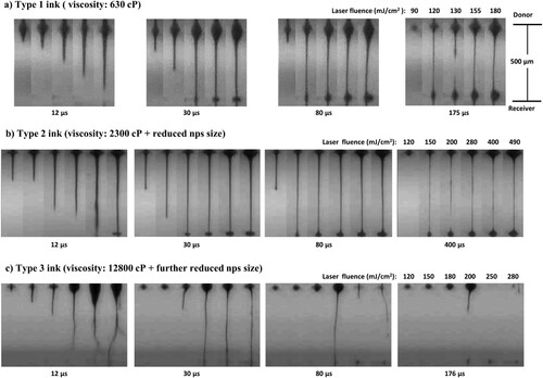
A high speed imaging setup was designed and implemented in order to accurately capture the jets formation and propagation caused by laser irradiation and is thoroughly described in (Kalaitzis et al. Citation2019), given the high velocities (5 m/s) involved and the micron scale area of the phenomenon. The setup comprised of a high speed camera (Mini AX-100, Photron), capable of capturing 170,000 fps with a shutter speed of 1 µs, placed on the axis perpendicular to the printing direction, while the gap between the donor and the receiver was set at 500 µm.
2.4. Donor substrates for LIFT process
The preparation of the donor substrates involved in the printing process was performed prior to each experiment and according to previous studies (Tsakona et al. Citation2020), by coating a 10–12 µm thin film of the printable ink via an adjustable micrometer film applicator (Coatmaster 510, Multicator 411, Erichsen) onto a 1 mm thick rectangular quartz substrate (15 cm length) purchased from UQG Optics.
2.5. Silver nanoparticle inks
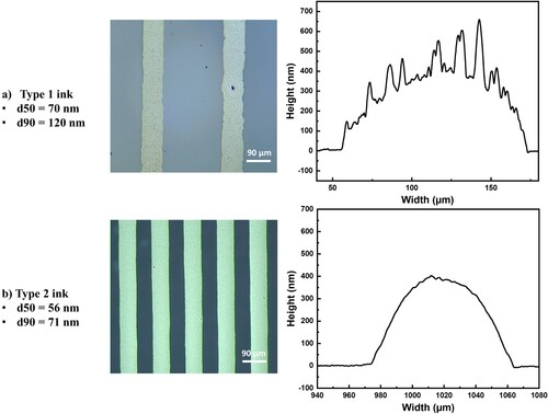
The three non Newtonian Ag nanoparticle high viscosity inks investigated in this study for the gate electrode fabrication were developed based on single-crystal silver NPs in an organic solvent tailored for the LIFT process and laser sintering by P.V. Nano Cell Ltd. (Migdal HaEmek, Israel), featuring a solid content of 70% wt, with a resulting viscosity value which ranges between 635 and 12, 800 cP at shear rate 1sec-1 as seen in . Those differences in the viscosity value can be attributed to the decrease of nanoparticle size and the consequent increase of the surface area (Bao et al. Citation2019). These inks were characterised by such viscosity values so that high throughput and narrow patterning on plastic and glass substrates were facilitated (line width ∼ 50 µm, height ∼ 0.5 µm and spacing∼ 50 µm), considering the diverse wetting properties of the substrates. Apart from the viscosity, each ink was distinguished in terms of nanoparticle size distribution, as indicated in . The 5 first ink (Type 1) had a measured viscosity value of 632 cP with a nanoparticle size range between 30 and 180 nm and a broad nanoparticle size distribution (a). The second ink (Type 2) had a viscosity value of 2300 cP with a nanoparticle size range between 35 − 85 nm and a reduced nanoparticle size distribution (b). Finally, The third ink’s (Type 3) viscosity value was measured at 12,800 cP with a nanoparticle size range between 30 − 70 nm and a further reduced nanoparticle size distribution (c). Additionally, the most viscous ink (type 3) dispersion, included special additives for the improvement of the resistivity value after the sintering process.
Figure 3. Three nanoparticle inks exhibiting differences regarding the nanoparticle size distribution and the viscosity value and the corresponding scanning electron microscope images (a) ink exhibiting standard nanoparticle size and distribution (Type 1) (b) ink with reduced nanoparticle size and distribution (Type 2) (c) ink with further reduced nanoparticle size and distribution (Type 3).
Table 1. Properties of the Ag inks utilised in the experiments.
3. Results and discussion
The identification of the key challenges for the manufacturing of high-performance electronics, such as a functional OTFT gate electrode, exposes crucial characteristics such as printing resolution, electrical performance and yield of the multi composite electronics (Kong et al. Citation2014). Unexpected non uniformity of the printed structures thickness could result in a low yield which can affect the consistency of the printed components and the process reproducibility. Also, the occurrence of a short-circuit between the conductive layers of the top and bottom of the whole stack within multilayered electronics due to the non uniformity, or the deterioration induced by a post printing treatment process, pose another challenge of additive manufactured electronics (Ko et al. Citation2007). Thus, a number of important parameters affecting the device’s performance were investigated. Firstly, the conductive deposited material achieved promising resistivity values after thermal treatment (∼2–3 times ×bulk). Also, the uniformity and homogeneity of the printed patterns were confirmed with profile measurements (410 nm height with a standard deviation of 35 nm) additionally to the compatibility of the thermal process employed with the sensitive substrate of interest (25 µOhm ∗ cm with a standard deviation of 4 µOhm ∗ cm with no short circuit evidence between the layers). Finally, an organic semiconductor electrical evaluation between LIFT and sputtering fabricated OTFT stacks was performed.
3.1. Oven and laser sintering investigation on films for defining the resistivity limit
Regarding the resistivity investigation conducted on three film coated Ag inks of 1.5 µm thickness, commercially available quartz slides of 1.1 mm thickness were used as substrates, due to their thermal durability (Tg > 500 oC) even for higher laser sintering powers. Thus, undesired substrate dependent thermal effects were avoided. Subsequently, these substrates were sintered using a broad range of laser fluence values. For comparison, film coated Ag inks of the same characteristics were also sintered with the utilisation of an oven for elevated temperature treatment. For the electrical characterisation of laser sintered micro-patterns and film coated Ag inks, a four point probe IV station implementing the Van Der Pauw method was utilised. Thus, oven and laser sintering processes were compared. Four different values (150, 200, 250 and 300 oC) of oven temperatures for 1 h treatment were selected as well as five laser sintering powers (300, 500, 850, 1250 mW). Thus, the laser treatment could be correlated to the oven’s quantitatively. As demonstrated in , all three inks exhibit excellent resistivity values (2–3 times x Bulk) both in the case of laser sintering 4b and oven sintering method 4a. In the case of inks comprising of nanoparticles exhibiting sizes smaller than 10 nm, the resistivity values can be attributed mainly to the nanoparticle’s size (Son et al. Citation2011). In our case, inks with a nanoparticle size distribution in the range from 50 to 200 nm were employed 1, thus an emerging crucial characteristic was the amount of the polymeric protective agent of these silver nanoparticles (Mo et al. Citation2019). Considering this, the reason that the further reduced nanoparticle size ink (Type 3) exhibited the best performance regarding the resistivity values (3 µOhm ∗ cm with a standard deviation of 0.5 µOhm ∗ cm) can be attributed not only to the fact that it comprised nanoparticles with a smaller nanoparticle size, but also to the utilisation of laser sintering additives during the production of the ink. The resistivity value comparison of the two inks without additives, namely the Type 1 and Type 2 inks revealed that the former, namely the ink with the larger nanoparticles additionally to a larger nanoparticle size distribution ((a)), presented lower resistivity values both for low oven sintering temperatures (a) and laser sintering powers (b). This feature can be attributed to the existence of a broad nanoparticle size distribution which enabled the successful formation of necking between the nanoparticles, as indicated by the scanning electron microscope images (a,b). Apparently, with the implementation of large laser sintering powers and oven temperature values, all three inks investigated converge to the same resistivity value. The aforementioned results confirmed that these three inks could be potential candidates for the fabrication of conductive patterns for an OTFT device.
Figure 4. Resistivity investigation graphs and corresponding scanning electron microscope images of Ag inks films with 1.5 µm thickness (a) Oven temperature baking process and (b) laser sintering process.
3.2. Digital processing: laser printing and laser sintering of conformal patterns
For the validation of the ability of a successful pattern fabrication exhibiting high yield reliability, printing of demanding design multi-component patterns on planar substrates was performed. The deposited material of choice was the Type 2 ink, which was selected while taking into consideration a number of important characteristics. The first involved the stability of the jet formation during the printing experiments. After a quantitative optical investigation regarding the jet’s formation and propagation using a high-speed camera as in (Kalaitzis et al. Citation2019), it became apparent that the Type 3 ink, although great in terms of resistivity even with the utilisation of small laser sintering power, could not demonstrate a stable reproducible jet capable of forming linear continuous printed lines (c). The aforementioned characteristic could be attributed to the further reduced nanoparticles’ size and size distribution, features which affect the rheological behaviour of the ink. On the contrary, the other two inks (Type 1 and Type 2) exhibited a stable jet for the material transferring (a,b).
Figure 5. High speed imaging for the evaluation of the rheological behaviour-jetting for (a) standard nanoparticle size ink (b) reduced nanoparticle size ink (c) further reduced nanoparticle size ink.
Consequently, for the investigation of the printed sample’s homogeneity, the Type 1 and 2 inks were used for the fabrication of straight lines. A great number of experimental sets indicated the optimised printing parameters for these two inks for the fabrication of straight printed lines: fluence 135 mJ/cm2, spot to spot distance 45 µm and a laser spot size of 35 µm. The distance between the donor and the receiver was set at 100µm. While evaluating the homogeneity of the printed lines with the utilisation of profile measurements, another decisive parameter emerged was the nanoparticle size distribution, a characteristic responsible for the occurrence of hundred nms height spikes on top of the printed lines, especially for Type 1 ink (a). This feature resulted in printed lines with insufficient morphological homogeneity, contrary to the line morphology exhibited by the Type 2 ink (b).
Figure 6. Microscope photos and profile measurements for (a) Type 1 d50 = 70 nm d90 = 120 nm ink (b) Type 2 ink d50 = 56 nm d90 = 71 nm.
3.2.1. Printing of multi-component linear patterns
The aforementioned resistivity, printability and homogeneity studies highlighted the Type 2 ink as the material of choice for the fabrication of the printed patterns. Utilising the same laser parameters for printing as mentioned above, complex designs were fabricated (a), which exhibited a width of 85 µm with a standard deviation (std) of 5 µm and a line thickness of 410 nm with a low std of 35 nm , as indicated by profile measurements (b). Due to the complex morphology and wetting properties of this particular substrate and the specific rheological characteristics of the ink utilised, the minimum line width value was increased compared with some of the author’s previous works (Zacharatos et al. Citation2016). Nevertheless, the resulting lines form factors (width, length and height) were specified so as to deliver functional OTFTs with integrated gate drivers. The demanding design consisted of straight lines of multiple lengths ranging from 40 µm up to 5 mm. In addition, peel-off tests evaluating the OTFT stack following the printing process were carried out. The adhesion of the laser printed lines ranged from 0.39 to 7.87 N/cm. In these range tested no delamination nor crack issues were detected. The selection of this design validated the versatility of the LIFT technique regarding the drop on demand digital maskless transfer of materials.
Figure 7. LIFT printed patterns on flexible substrates (a) Demanding design printed on planar flexible dielectric (b) Profile measurements of printed lines.
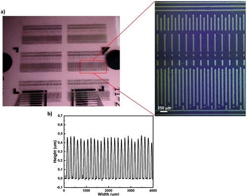
Table 2. Morphological properties and adhesion behaviour of laser printed and laser sintered lines.
3.2.2. Conformal printing and sintering of 3 cm long conductive lines on fully patterned substrates
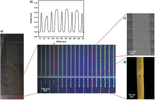
After the verification via the complex design fabrication, laser printed 3 cm long conductive lines (a) of the same morphological characteristics as the multicomponent linear patterns were fabricated, with the same laser printing parameters as in 3.2.1. The non planar substrates consisting of metallic structures underneath the spin coated gate dielectric exhibited a periodic pattern of hills and valleys with height up to 200 nm, as indicated by profile measurements conducted prior to the printing process (b). As confirmed by the scanning electron microscope (c), the LIFT process accomplished the conformal printing and sintering of conductive ink on non-planar substrates while the thermally sensitive gate dielectric substrate remained intact. Also, the printing process enabled the connection of the non planar gate electrode active area with dedicated electrical components for the interconnection of the device (d). For the necessary laser sintering process, a laser power of 160 mW along with a laser spot of 60 µm and a spatial overlap of 98% was employed. As a result, conductive lines with resistivity values of 25 µOhm ∗ cm with an std of 4 µOhm ∗ cm were fabricated. No evidence of short circuit between the conductive lines and the patterned metallic structures under the gate dielectric was detected.
Figure 8. LIFT printed patterns on flexible substrates (a) Conformal LIFT printed and sintered 3 cm on non planar flexible substrate (b) Prior to the printing process profile measurement of the non planar substrate (c) corresponding scanning electron microscope image (d) successful connection of the non planar active area with electrical components.
Compared to the Ag films on quartz resistivity investigated, these distinct resistivity values of the conductive lines could be explained by the unique morphology of the printed lines and the different thermal properties the fully patterned multilayered samples exhibit . More specifically, these particular laser sintering parameters were employed due to the sensitivity of the gate dielectric and also taking into consideration the heat confinement this special material exhibits, a feature that justifies the employment of smaller laser powers for the sintering process ().
Table 3. Resistivity values comparison for Type 2 ink for laser sintering.
3.3. Organic semiconductor proof of concept
For the demonstration of the potential application of the laser printing process for a functional device, organic thin-film transistors were fabricated up to the gate dielectric using in house materials by FlexEnable. All devices have a bottom contact top gate structure and utilise an organic semiconductor (OSC) material and a gate dielectric. The source and drain bottom contacts were fabricated by photolithography and the OSC and organic gate dielectric were deposited by spin coating. Laser printed gate exhibiting a width of 680 µm with a std 30 µm, a height of 730 nm with a std 50 nm and a maximum length of 7.1 mm with a std of 30 µm were printed on top of the gate dielectric, as shown in (a). The laser parameters for the printing and sintering processes employed were as mentioned above. The electrical test station for the evaluation of the OSC performance demanded a sample of larger width compered to the printed lines as presented on 3.2.2 (680 and 85 µm respectively). Thus, the printing of consecutive lines resulted on a thicker printed sample (730 nm instead of 410 nm). The electrical performance of the LIFT printed and sintered OTFT devices was compared to a sputtered gate process at FlexEnable using the same OTFT stack (b,c).
Figure 9. (a) Microscope image of an OTFT device using a laser printed gate (b) Transfer curves measurements for devices with LIFT printed and sintered gate (c) Transfer curves measurements for devices with sputtering deposited gate.
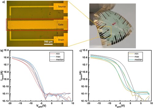
Several OTFT devices were measured at drain voltage V d = −1 V . On average, the resulting electron mobility only decreased for 10% from 1 cm2/(V.s) (using a gate sputtering process) to 0.9 cm2/(V.s) (using laser digital processing). Also, as indicated by the graphs, Vth increased by less than 5 V while the Ion reduced by less than 50%. This proves that the OSC endures the fabrication process. The overall performance of the OTFTs using a laser printed gate appears to be similar to that made by sputtered gate process, with a 50% drop off. This demonstrates the low impact of the laser processing on the OTFT performances. Additionally, life time performance tests for the OTFTs at the device level were carried out. The devices demonstrated acceptable stability under aging test (90 °C bake for 18 h) with degradation of Ion less than 50%.
4. Conclusions
In this work, the fabrication of OTFT gate electrodes with the employment of LIFT was achieved on top of fully patterned substrates in a hybrid processing scheme involving also standard microelectronic processes. Initially, a resistivity investigation was conducted between 3 types of silver nanoparticles inks, which confirmed the ability of forming conductive patterns with great electrical performance (∼2–3 times × bulk resistivity values). The aforementioned inks were also investigated in terms of printability and homogeneity, a process that indicated that Type 2 ink was the material of choice. Thus, patterns exhibiting a complex design and advanced morphological homogeneity (410 nm height with a std of 35 nm) were printed on planar substrates. Additionally, 3 cm long conductive lines were fabricated on top of non planar substrates displaying resistivity values of 25 µOhm ∗ cm with an std of 4 µOhm ∗ cm. For the verification of the process compatibility with the organic semiconductor and the low Tg gate dielectric, the fabrication of test structures enabled the electrical performance evaluation. Therefore, by reporting an overall OSC electrical performance drop of less than 50% in comparison with a traditional fabrication technique, the laser process was validated an excellent candidate for the manufacturing of gate electrodes on top of multilayered sensitive stacks.
Disclosure statement
No potential conflict of interest was reported by the author(s).
Correction Statement
This article has been corrected with minor changes. These changes do not impact the academic content of the article.
Additional information
Funding
Notes on contributors
Kostas Andritsos
Kostas Andritsos is a PhD candidate in the physics department of NTUA. He received his diploma in School of Applied Mathematical and Physical Science, Physics Department from the National Technical University of Athens in 2018. He has been working as a junior researcher within the framework of EC and national-funded projects. His research focuses on the printing of materials in the liquid phase for microelectronics applications and functional devices in the flexible state. He is the co-author of 5 publications in peer-reviewed scientific journals and has participated in a number of international conferences.
Ioannis Theodorakos
Ioannis Theodorakos is currently a postdoctoral researcher in the physics department of NTUA. He received his diploma in School of Applied Mathematical and Physical Science, Physics Department from the National Technical University of Athens in 2010, and his Master degree in Microsystems and Nanodevices at the National Technical University of Athens in 2012. In 2019 he received the Ph.D. degree specializing in laser printing and materials laser processing from the Physics department of the National Technical University of Athens. He has been working as a junior researcher within the framework of EC and national-funded projects. His research focuses on the printing of materials in the liquid phase for microelectronics application and the laser treatment of inorganic materials. He is the co-author of 12 publications in peer- reviewed scientific journals and 5 publications in conference proceedings.
Filimon Zacharatos
Filimon Zacharatos was born in Athens, Greece in 1981. He received the Physics diploma from Patras University in 2003 and the Ph.D. degree, specializing in nanotechnology, from the Physics department of (NTUA) in 2009. Until 2009, he had been working at the Institute of Microelectronics, of the National Center for Scientific Research Demokritos in Athens, as a Ph.D. researcher, investigating nanostructured materials for applications in Microelectronics and RF systems. Between 2011 and 2013 he worked in the field of Plasmonics and their applications in telecom waveguides and optical switches, as a postdoctoral fellow in the sub-micron optics group of CNRS, University of Burgundy. Dr. Filimon Zacharatos is currently a postdoctoral researcher in the physics department of the National Technical University of Athens (NTUA), working within the framework of EC and national funded projects. His current research interests are mostly focused on the laser processing of thin metal films and nanomaterials for applications in optoelectronics and flexible electronics. He is the author or the co-author of 22 publications in peer-reviewed scientific journals, of 1 book chapter and the co-inventor of 2 patents.
Ayala Kabla
Ayala Kabla, project manager at PV Nano cell, has over fifteen years of industrial experience in nano materials and nano technologies, project management and research in addition to research in semiconductors for solar cells, currently leading the EC and national funded projects at PV Nano Cell. Holds M.S. and B.S. degrees in Materials Science and Engineering from Carnegie Mellon University (Pittsburgh, USA).
Semyon Melamed
Semyon Melamed, the chief chemist at PV Nano Cell, has extensive development, preparation and up-scaling experience in conductive inks for inkjet, aerosol, and laser printing. In-depth experience with polymers, polymeric composites, organic/inorganic hybrid materials, ceramic materials and sol-tel tchnology. Holds a M.Sc. in Chemistry from the Technion Institute of Technology, and M.Sc. in Chemical Engineering from the Institute of Fine Chemical Technology in Moscow.
Fernando de la Vega
Fernando de la Vega, the Chief technology officer and Founder of PV Nano Cell, has over 30 years of experience in the industry with large network and great reputation. Vast experience in management and operations. Holds a PhD in applied chemistry (Casali Institute, The Hebrew University).
Yoann Porte
Yoann Porte was born in Tours, France in 1988. In 2012, he obtained his Masters degree in Nano and Micro Technologies from the Ecole Nationale Suprieur de Chimie, Biologie et Physique (ENSCBP) in Bordeaux, France. Between 2012 and 2016, he completed his Ph.D degree at Imperial College London, UK, in materials science. His main research focused on thin film metal oxide semiconductors for opto-electronic applications using pulsed laser deposition as deposition process. In 2017, he joined Yonsei University in South Korea as a Post-doctoral fellow for a year and a half. His work involved the development of inorganic perovskite quantum dots and their integration in inorganic light emitting devices. Dr. Yoann Porte is currently working as a senior research engineer at FlexEnable. His work involves the development of dielectric materials for Thin Film Transistors and display applications. He is the author and co-author of 12 publications in peer-reviewed scientific journals.
Patrick Too
Dr. Patrick Too is a Senior Principal Project Lead at FlexEnable. He has over 18 years experiences working in plastic electronics projects that cross many disciplines from organic transistors, sensors and LC optics. He has long term experience leading and participating in both UK and EC funded projects. Holds a PhD in Physical Science and Engineering from University of Surrey.
Ioanna Zergioti
Ioanna Zergioti is a Professor at the National Technical University of Athens, School of Applied Mathematics and Physical Sciences. In the framework of her PhD work she worked for the fall semester of 1996 in the Mechanical Engineering Department at the University of California, Berkeley on the Laser Induced Forward Transfer process. After her PhD, she worked as a post doctoral researcher in the Max Planck Institut fr Biophysikalische Chemie in Gttingen, on Laser matter interactions studies. Then, she worked as a post-doctoral researcher in the Philips CFT on Laser Sintering of sol gels for electronics until 2000. She was a researcher for 4 years (1999-2003) at the Laser Applications Division of the Institute of Electronic Structure and Laser FORTH, where she developed works on ultrashort laser microstructuring (etching and printing) of metals, oxides and biomaterials. Since September 2003 she was appointed at the National Technical University of Athens, School of Applied Mathematical and Physical Sciences and since 2018 she is a Professor. Her main activities are related to the laser microprinting of biological molecules and laser matter interaction studies for biotechnological applications and organic electronics.
References
- Andritsos, Kostas, Ioannis Theodorakos, Filimon Zacharatos, and Ioanna Zergioti. 2020. “The Effect of Electromigration on the Lifetime and Performance of flexible Interconnections Fabricated by Laser Printing and Sintering.” Applied Surface Science 506: 144968.
- Bao, L., C. Zhong, P. Jie, and Y. Hou. 2019. “The Effect of Nanoparticle Size and Nanoparticle Aggregation on the Flow Characteristics of Nanofluids by Molecular Dynamics Simulation.” Advances in Mechanical Engineering 11 (11): 1687814019889486.
- Birnbaum, Andrew J, Heungsoo Kim, Nicholas A. Charipar, and Alberto Pique. 2010. “Laser Printing of Multi-Layered Polymer/Metal Heterostructures for Electronic and MEMS Devices.” Applied Physics A 99 (4): 711–716.
- Bolduc, M., C. Trudeau, P. Beaupr, S. G. Cloutier, and P. Galarneau. 2018. “Thermal Dynamics Effects Using Pulse-Shaping Laser Sintering of Printed Silver Inks.” Scientific Reports 8. https://pubmed.ncbi.nlm.nih.gov/29362423/.
- Coelho, J., M. P. Kremer, S. Pinilla, and V. Nicolosi. 2020. “An Outlook on Printed Microsupercapacitors: Technology Status, Remaining Challenges, and Opportunities.” Current Opinion in Electrochemistry 21: 69–75.
- Constantinescu, C., A. K. Diallo, L. Rapp, P. Cremillieu, R. Mazurczyk, F. Serein-Spirau, J. P. Lere-Porte, P. Delaporte, A. P. Alloncle, and C. Videlot-Ackermann. 2015. “Laser-induced Forward Transfer of Multi-Layered Structures for OTFT Applications.” Applied Surface Science 336: 11–15.
- Constantinescu, Catalin, Ludovic Rapp, Philippe Delaporte, and Anne Patricia Alloncle. 2016. “Investigations on Laser Printing of Microcapacitors Using Poly (Methyl Methacrylate) Dielectric Thin films for Organic Electronics Applications.” Applied Surface Science 374: 90–95.
- Dang, Wenting, Libu Manjakkal, William Taube Navaraj, Leandro Lorenzelli, Vincenzo Vinciguerra, and Ravinder Dahiya. 2018. “Stretchable Wireless System for Sweat pH Monitoring.” Biosensors and Bioelectronics 107: 192–202.
- Fukuda, Kenjiro, and Takao Someya. 2017. “Recent Progress in the Development of Printed Thin-film Transistors and Circuits with High-Resolution Printing Technology.” Advanced Materials 29 (25): 1602736.
- Giannakou, Pavlos, Mateus G Masteghin, Robert CT Slade, Steven J Hinder, and Maxim Shkunov. 2019. “Energy Storage on Demand: Ultra-High-Rate and High-Energy-Density Inkjetprinted NiO Micro-Supercapacitors.” Journal of Materials Chemistry A 7 (37): 21496–21506.
- Guo, S. C., and C. Singh. 2021. Handbook of Laser Technology and Applications: Lasers Applications: Materials Processing and Spectroscopy (Volume Three). CRC Press.
- Han, Tao, Sudip Kundu, Anindya Nag, and Yongzhao Xu. 2019. “3D Printed Sensors for Biomedical Applications: A Review.” Sensors 19 (7): 1706.
- Hanitra, Ivan Ny, Lucia Lobello, Francesca Stradolini, Abuduwaili Tuoheti, Francesca Criscuolo, Tugba Kilic, Danilo Demarchi, Sandro Carrara, and Giovanni De Micheli. 2018. “A Flexible Front-End for Wearable Electrochemical Sensing.” MeMeA 2018 IEEE International Symposium on Medical Measurements and Applications, Proceedings 558–563. https://infoscience.epfl.ch/record/256367.
- Kalaitzis, A., M. Makrygianni, I. Theodorakos, A. Hatziapostolou, S. Melamed, A. Kabla, F. de la Vega, and I. Zergioti. 2019. “Jetting Dynamics of Newtonian and non-Newtonian fluids via Laser-Induced Forward Transfer: Experimental and Simulation Studies.” Applied Surface Science 465: 136–142.
- Kattamis, Nicholas T., Neil D. McDaniel, Stefan Bernhard, and Craig B. Arnold. 2011. “Ambient Laser Direct-Write Printing of a Patterned Organo-Metallic Electroluminescent Device.” Organic Electronics 12 (7): 1152–1158.
- Kim, Chiyen, David Espalin, Min Liang, Hao Xin, Alejandro Cuaron, Issac Varela, Eric Macdonald, and Ryan B. Wicker. 2017. “3D Printed Electronics with High Performance, Multi-Layered Electrical Interconnect.” IEEE Access 5: 25286–25294. https://arizona.pure.elsevier.com/en/publications/3d-printed-electronics-with-highperformance-multi-layered-electr.
- Ko, Seung H., Heng Pan, Costas P. Grigoropoulos, Christine K. Luscombe, Jean M.J. Frchet, and Dimos Poulikakos. 2007. “All-inkjet-printed flexible Electronics Fabrication on a Polymer Substrate by low-Temperature High-Resolution Selective Laser Sintering of Metal Nanoparticles.” Nanotechnology 18: 345202. doi:10.1088/09574484/18/34/345202.
- Ko, Seung Hwanmax, Heng Pan, Daeho Lee, Costas P. Grigoropoulos, and Hee K. Park. 2010. “Nanoparticle Selective Laser Processing for a flexible Display Fabrication.” Japanese Journal of Applied Physics 49: 05EC03. doi:10.1143/JJAP.49.05EC03.
- Kong, Yong Lin, Ian A Tamargo, Hyoungsoo Kim, Blake N Johnson, Maneesh K Gupta, TaeWook Koh, Huai-An Chin, Daniel A Steingart, Barry P Rand, and Michael C McAlpine. 2014. “3D Printed Quantum dot Light-Emitting Diodes.” Nano Letters 14 (12): 7017–7023.
- Koritsoglou, O., I. Theodorakos, F. Zacharatos, M. Makrygianni, D. Kariyapperuma, R. Price, B. Cobb, et al. 2019. “Copper Micro-Electrode Fabrication Using Laser Printing and Laser Sintering Processes for on-Chip Antennas on flexible Integrated Circuits.” Optical Materials Express 9 (7): 3046–3058.
- Kumar, Sanjay, Pulak Bhushan, Mohit Pandey, and Shantanu Bhattacharya. 2019. “Additive Manufacturing as an Emerging Technology for Fabrication of Microelectromechanical Systems (MEMS).” Jt 2: 175–197. doi:10.1177/2516598419843688.
- Lee, Sung Min, Jeong Hyun Kwon, Seonil Kwon, and Kyung Cheol Choi. 2017. “A Review of Flexible OLEDs Toward Highly Durable Unusual Displays.” IEEE Transactions on Electron Devices 64: 1922–1931.
- Makrygianni, M., I. Kalpyris, C. Boutopoulos, and I. Zergioti. 2014. “Laser Induced Forward Transfer of Ag Nanoparticles ink Deposition and Characterization.” Applied Surface Science 297: 40–44.
- Manikam, Vemal Raja, and Kuan Yew Cheong. 2011. “Die Attach Materials for High Temperature Applications: A Review.” IEEE Transactions on Components, Packaging and Manufacturing Technology 1 (4): 457–478.
- Markey, Laurent, Filimon Zacharatos, Jean Claude Weeber, Andreas Prinzen, Michael Waldow, Michael G. Nielsen, Tolga Tekin, and Alain Dereux. 2015. “Recess Photomask Contact Lithography and the Fabrication of Coupled Silicon Photonic and Plasmonic Waveguide Switches.” Microelectronic Engineering 141: 129–134.
- Mo, Lixin, Zhenxin Guo, Zhenguo Wang, Li Yang, Yi Fang, Zhiqing Xin, Xiu Li, et al. 2019. “Nano-silver ink of High Conductivity and low Sintering Temperature for Paper Electronics.” Nanoscale Research Letters 14 (1): 1–11.
- Morales, M., D. Munoz-Martin, A. Marquez, S. Lauzurica, and C. Molpeceres. 2018. “LaserInduced Forward Transfer Techniques and Applications.” Advances in Laser Materials Processing Technology, Research and Applications, 339–379. https://doi.org/10.1016/C2015-0-05718-5
- Piqu, Alberto, Heungsoo Kim, Raymond C.Y. Auyeung, Iyoel Beniam, and Eric Breckenfeld. 2016. “Laser-induced Forward Transfer (LIFT) of Congruent Voxels.” Applied Surface Science 374: 42–48.
- Rother, Marcel, Maximilian Brohmann, Shuyi Yang, Stefan B Grimm, Stefan P Schießl, Arko Graf, and Jana Zaumseil. 2017. “Aerosol-Jet Printing of Polymer-Sorted (6, 5) Carbon Nanotubes for Field-Effect Transistors with High Reproducibility.” Advanced Electronic Materials 3 (8): 1700080.
- Son, Yong, Junyeob Yeo, Hanul Moon, Tae Woo Lim, Sukjoon Hong, Koo Hyun Nam, Seunghyup Yoo, Costas P. Grigoropoulos, Dong Yol Yang, and Seung Hwan Ko. 2011. “Nanoscale Electronics: Digital Fabrication by Direct Femtosecond Laser Processing of Metal Nanoparticles.” Advanced Materials 23: 3176–3181. https://onlinelibrary.wiley.com/doi/abs/10.1002adma.201100717.
- Suganuma, Katsuaki, Seong-Jun Kim, and Keun-Soo Kim. 2009. “High-Temperature Lead-Free Solders: Properties and Possibilities.” JOM – Journal of the Minerals, Metals and Materials Society 61 (1): 64.
- Sun, Jeong-Yun, Christoph Keplinger, George M Whitesides, and Zhigang Suo. 2014. “Ionic Skin.” Advanced Materials 26 (45): 7608–7614.
- Theodorakos, Ioannis, Agamemnon Kalaitzis, Marina Makrygianni, Antonios Hatziapostolou, Ayala Kabla, Semyon Melamed, Fernando de la Vega, and Ioanna Zergioti. 2019. “LaserInduced Forward Transfer of High Viscous, NonNewtonian Silver Nanoparticle Inks: Jet Dynamics and Temporal Evolution of the Printed Droplet Study.” Advanced Engineering Materials 1900605: 1900605. doi:10.1002/adem.201900605.
- Tsakona, D., I. Theodorakos, A. Kalaitzis, and I. Zergioti. 2020. “Investigation on High Speed Laser Printing of Silver Nanoparticle Inks on flexible Substrates.” Applied Surface Science 513: 145912.
- Wu, Zhigang, Yongan Huang, and Rong Chen. 2017. “Opportunities and Challenges in flexible and Stretchable Electronics: A Panel Discussion at ISFSE2016.” Micromachines 8.
- Zacharatos, F., M. Makrygianni, R. Geremia, E. Biver, D. Karnakis, S. Leyder, D. Puerto, P. Delaporte, and I. Zergioti. 2016. “Laser Direct Write Micro-Fabrication of Large Area Electronics on flexible Substrates.” Applied Surface Science 374: 117–123.
- Zacharatos, F., I. Theodorakos, P. Karvounis, S. Tuohy, N. Braz, S. Melamed, A. Kabla, et al. 2018. “Selective Laser Sintering Of Laser Printed Ag Nanoparticle Micropatterns at High Repetition Rates.” Materials 11 (11): 2142.
- Zhang, Suoming, Le Cai, Tongyu Wang, Jinshui Miao, Nelson Sepulveda, and Chuan Wang. 2017. “Fully Printed Flexible Carbon Nanotube Photodetectors.” Applied Physics Letters 110 (12): 123105.
- Zhou, Honglei, Weiyang Qin, Qingmin Yu, Huanyu Cheng, Xudong Yu, and Huaping Wu. 2019. “Transfer Printing and Its Applications in Flexible Electronic Devices.” Nanomaterials 9: 283. https://www.mdpi.com/2079-4991/9/2/283/htm.
