
 ?Mathematical formulae have been encoded as MathML and are displayed in this HTML version using MathJax in order to improve their display. Uncheck the box to turn MathJax off. This feature requires Javascript. Click on a formula to zoom.
ABSTRACT
Electromagnetic pollution and military stealth technique have raised tremendous interest in high-performance microwave-absorbing structures. However, an ultra-broadband absorbing functional structure is still in urgent demand. Herein, a novel continuous conductive fibre-based absorbing metamaterial was successfully designed and fabricated by multi-materials hybrid 3D printing technique. Benefitting from the highly symmetric structured design of a super unit cell and appropriate conductive property of continuous fibre, the absorbing metamaterial is demonstrated to have an ultra-wide band microwave absorption and polarisation insensitivity. Furthermore, the thickness of the proposed metamaterial is only 3.2 mm of 0.085λmax. In the wave absorption test, the metamaterial shows a broadband absorption of 8–18.1 GHz (greater than 90%) and maintains a good absorption effect at an incident angle of 40°. The design and fabrication method of the continuous fibre-absorbing metamaterial provides a new idea for the realisation of the integrated bearing and absorbing metamaterial, which will greatly promote the practical application of absorbing metamaterial.
1. Introduction
A metamaterial absorbing structure can achieve excellent absorbing performance through the artificial design of subwavelength elements [Citation1,Citation2], which is an important way to solve the problem of information leakage, equipment accuracy decline, and human health damage caused by electromagnetic radiation and electromagnetic interference [Citation3,Citation4]. Numerous research studies have been demonstrated to increase the absorbing performance of metamaterials [Citation5]. Metal-based absorbing metamaterials can show nearly 100% absorbance at the specific resonant frequency or several discretised frequencies [Citation6,Citation7]. In addition, the combination of adjacent resonant frequency points can be realised by multilayer laminated manufacturing of metal and dielectric layers to broaden the bandwidth, but it has a large structural thickness [Citation8]. It is common to use lumped resistors loaded on resonators to increase absorption bandwidth [Citation9]. However, the use of high-frequency resistors to achieve ohmic losses has high cost, and the actual resistance shape and the welding process have adverse effects on the absorbing performance [Citation10]. All dielectric metastructure can realise excellent broadband microwave absorption [Citation11,Citation12], still facing the challenge of bulky volume and lightweight. A metamaterial absorber with thin thickness and ultra-bandwidth that can be prepared easily is urgently needed.
Continuous fibres have attracted much attention because of their outstanding mechanical properties, chemical stability and excellent environmental adaptation [Citation13]. However, the commonly used metal fibres and carbon fibres are harder to be directly applied for electromagnetic absorption because of their high conductivity, which makes them a strong reflector of electromagnetic waves [Citation14]. Previous studies have focused on the application of continuous fibres to simple-shaped frequency-selective surfaces [Citation15–17] or on the use of scattering mechanisms to reduce radar cross section (RCS) [Citation18,Citation19]. It is hard to overcome the detective challenge of multistation radar. The more complex pattern and fine design of metamaterials can provide higher electromagnetic wave manipulation performance of the structure [Citation20,Citation21]. Fortunately, continuous fibre 3D printing provides the possibility of preparing metamaterials. The multi-materials hybrid 3D printing process integrates continuous filament bundles into the polymer matrix for co-extrusion [Citation22]. This printing method can improve the strength compared with pure matrix extrusion printing [Citation23–25] and has been able to realise the lightweight of some structures [Citation26]. Coated fibres with suitable electrical conductivity can provide ohmic losses for electromagnetic wave absorption [Citation15]. To date, a continuous conductive fibre metamaterial for high-efficiency microwave absorption is still lacking.
We propose a novel continuous fibre absorbing metamaterial, which is realised by the multi-materials hybrid 3D printing. The arrangement and connection of helical element structure are designed by space-filling curves to reduce the polarisation sensitivity of the structure. The influence of the super unit with different numbers of units and continuous connection between units on the performance is studied. It is proved that the arrangement of elements based on space-filling curve is universal for continuous fibre metamaterial printing. The carbon nanotube-coated dacron fibres integrated polylactic acid (PLA) composite is fabricated on pure PLA substrate by multi-materials hybrid 3D printing. Simulations and experiments show that the use of continuous conductive fibres 3D printed metamaterials can achieve broadband electromagnetic absorption. The simplicity and flexibility of the fabricating process make our proposal more promising in shaping wideband and multifunctional absorber structures. The design and preparation of this metamaterial provide a new idea for the application of continuous fibres in absorbing metamaterial.
2. Structure design and impedance characteristics analysis
2.1. Structure design
shows a wave-absorbing metamaterial with a helical pattern arranged based on space-filling curves. The space-filling curve is a mapping function that maps high-dimensional spatial data to one-dimensional continuous space, which has the properties of successively traversing space and self-similarity [Citation27]. The Hibert curve provides a method for connecting non-centrosymmetric absorbing elements in different directions [Citation28]. Self-similarity allows the super unit with a smaller number of units to perform performance analysis instead of the entire sample. The properties of successively traversing space can not only avoid wire drawing in 3D printing [Citation29] but also is very suitable for the process characteristics of the multi-materials hybrid 3D printing with one stroke. As shown in (a), each element consists of a PLA dielectric substrate and continuous conductive fibres as a resistive layer. The pattern is composed of spirals connected by equidistant lines perpendicular to each other on the same plane. The integration of the curved conductive path in the metamaterial element can realise the miniaturisation of the absorbing unit and the resonance of multiple frequency points [Citation20], and the bandwidth can be further expanded by loading resistors on it. The selected helical structure not only has a long conductive path but also the start and end of a stroke path are located at both ends of the cell, which facilitates the use of space-filling curves to arrange the path. The connected helical structure can provide a larger equivalent inductance, which is beneficial to reducing the resonant frequency of the metamaterials. The geometric dimensions are optimised as follows: the unit side length p = 10 mm, the dielectric layer thickness h = 3.2 mm, the conductive pattern width t = 0.2 mm, the spacing is d and the centreline length s = 2.4 mm.
Figure 1. Structure diagram of a helical pattern metamaterial generated based on Hibert curve: (a) IU, (b) SU4, (c) SU16.
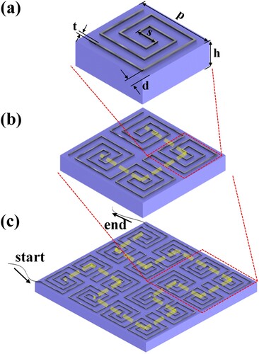
The method of generating Hibert curves filled with squares is used to arrange the angles and connections of absorbing elements. That is, a unit with a helical pattern is used as the initial unit (IU), which is taken as the lower left corner of the super unit including 4 units (SU4). The upper left corner pattern is obtained by rotating 90 clockwise. The remaining two are obtained in left-right mirror symmetry, and each unit is connected by a horizontal or vertical line. SU4 can then be used as the initial pattern again to get the super unit including 16 units (SU16). Repeat this iterative process until the desired size is reached. The dotted yellow line in illustrates the iterative process of the Hibert curve. Through the start and end points of SU16, it can be seen the connection order of the pattern and the characteristics of the formation of one stroke.
2.2. Equivalent model of conductive coated continuous fibre
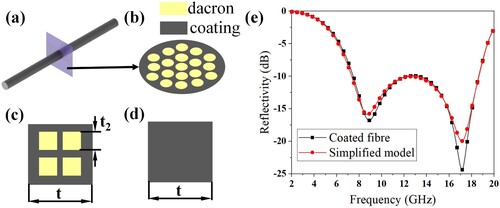
Unlike general resonant metamaterials, which consist of complete metallic conductors or uniformly resistive films, the centre of the carbon nanotube-coated fibre is an insulating polyester fibre . Therefore, it is necessary to carry out the equivalent model of the fibre material to ensure the accuracy of the subsequent structural optimisation. The formula for calculating the conductivity of the fibre is
(1)
(1) where
is the conductivity,
is the resistance test length,
is the resistance test value, and
is the conductive cross-sectional area. The real cross section of the fibre is similar to that shown in (b), but it is difficult to simulate the number and shape of the real fibre monofilaments. Therefore, (c) is used to represent the coated fibre, where
is the diameter of the coated fibre 0.2 mm and
is the diameter of the polyester fibre 0.05 mm. (d) shows a simplified cross-section model of the coated fibre, which no longer considers the insulating fibre in the centre of the fibre but is equivalent to a conductive material with uniform conductivity. On the premise that the resistance of the fibres of the same length is the same, the conductivity in (c) is 1067 S/m, and the conductivity in (d) is 800 S/m. Using the IU structure, the result in (e) shows that the wave absorption properties of both are almost identical, which proves that the insulating material in the coated fibre has little effect on the properties. This indicates that the non-conductive cavity in the coated fibre is very small and no resonant response can occur. The validity of the equivalent model proves that the conductive coating fibre can be treated as a uniform conductive material in microwave absorption [Citation15].
Figure 2. Equivalent cross-section model of coated fibre: (a) coated fibre, (b) true cross-section model of coated fibre, (c) coated fibre cross-section model, (d) equivalent fibre cross-section model; (e) Reflectance calculation of coated fibre and equivalent fibre in IU.
2.3. Equivalent circuit modelling
In order to study the mechanism of absorbing metamaterials, the equivalent circuit model was used for further analysis. An equivalent model is established in (a), where the equivalent impedance of the array layer is regarded as a series of capacitors, inductors and resistors, as shown in Equation (2). (b) shows that each line of the helical pattern can be equivalent to resistance and inductance, and the equivalent capacitance comes from the gap between adjacent line segments within the unit and the gap between adjacent units. The dielectric layer impedance
is shown in Equation (3), and the equivalent input impedance
is shown in Equation (4).
(2)
(2)
(3)
(3)
(4)
(4) where
is the dielectric constant of the dielectric layer, h is the dielectric layer thickness, c is the velocity of the electromagnetic wave in vacuum (c = 3 × 10⁸ m/s), f is the frequency of microwave, and
is the free-space impedance. The reflectance
is expressed as [Citation30]:
(5)
(5)
Figure 3. (a) Equivalent circuit of metamaterial with helical pattern; (b) equivalent circuit diagram of helical pattern.
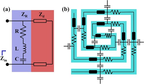
Therefore, by optimising the geometric parameters of the array layer to obtain appropriate R, L, C, reasonable can be adjusted to match the impedance in free space and high-efficiency absorption of the electromagnetic wave can be obtained. The equivalent resistance R is related to the material resistance and the pattern area, which is expressed as [Citation31]:
(6)
(6) where S is the area of the unit cell, A is the area of the array layer, t is the thickness of the array layer and
is the material conductivity. The equivalent inductance L is determined by the length of the conductor parallel to the incident electric field in the helical pattern, and the equivalent inductance C is determined by the gap between adjacent units and the gap between the helices. However, for more complex patterns, there is no exact equation to correspond to the relationship between geometric size and equivalent parameters, so we use the full-wave simulation method to obtain the equivalent parameters [Citation31]. The electromagnetic properties of the proposed helical absorbing metamaterial were investigated using CST Microwave Studio. The periodic boundary conditions are chosen in the X and Y directions, and the Z direction is an open boundary. The Floquet port acts as excitation to generate TE (transverse electric) and TM (transverse magnetic) plane waves. The equivalent parameters obtained by the full-wave simulation method are: R = 231 Ω, L = 1.26 nH, C = 0.109 pF. At the same time, resonance occurs when the imaginary part of
is equal to zero [Citation30], that is, the sum of
and
in Equation (4) is zero. Equation (3) is used to calculate the imaginary part
of the admittance of the PLA dielectric layer. The equivalent parameters are put into Equation (2) to calculate the imaginary part of the admittance
of the array layer. By optimising the parameters of the array layer, the first zero position of
and the zero position of
are almost equal. Then, the imaginary part of the input impedance has three zeros because
and
cancel out with the difference of positive and negative near the intersection point. (a) illustrates the equivalent susceptance of the array layer and the dielectric substrate, indicating that the absorbing metamaterial has three resonant frequency points between 2 and 20 GHz, providing the basis for wideband operation.
Figure 4. (a)Equivalent susceptance of the array layer and the dielectric substrate; (b) the reflectivity by circuit model and full-wave simulation.
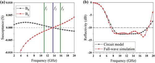
It can be seen from (b) that the reflectance calculated by the equivalent circuit model is very close to the results of full-wave simulation, which proves the effectiveness of the establishment of the equivalent circuit model. The continuous fibre wave-absorbing metamaterial achieves broadband wave absorption with the reflectance of 7.2–18.4 GHz below −10 dB with a thickness of 3.2 mm.
3. Experimental section
3.1. Materials and fabrication
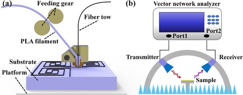
The electromagnetic absorbing metamaterial with a helical pattern was fabricated by the multi-materials hybrid 3D printing equipment (Shaanxi Fibretech Technology Development Co., Ltd, China). The conductive fibre array layer was prepared on a printed PLA substrate by in-situ impregnation method, as described in (a). In this printing process, continuous fibres and polymers are fed separately to the extruder. The heater in the extruder melts the polymer filament into a quasi-liquid state, and the fibre consolidates with the polymer for impregnation. Then, the consolidated fibre and the matrix are extruded from the nozzle and bonded to the substrate. Carbon nanotube-coated dacron fibres were used as conductive fibres (Produced by Zhejiang Rifang Nano Biotechnology Co., LTD). Its conductivity σ is 800 S/m and the fibre diameter is 0.2 mm. PLA was used as the substrate for continuous fibre printing and the dielectric layer of the absorbing unit. The specific printing parameters are as follows: the nozzle diameter is 0.8 mm, the printing thickness of the PLA layer is 0.3 mm, the printing temperature is 220°C. The fibre path is written by the Matlab program. The sample contains 18 × 18 units with a total size of 180 mm × 180 mm.
Figure 5. (a) Schematic of the continuous fibre 3D printing process; (b) reflectance measurement system.
3.2. Characterisation and measurement
The electromagnetic reflectivity of the fabricated helical metamaterial was conducted in an arch-free-space measurement system, as illustrated in (b). A dual rocker arm test stand and a vector network analyser (VNA, Ceyear AV3678D, China) were used to measure the reflection characteristics of the metamaterial samples. One of the two horn antennas in the operating frequency range of 1–20 GHz is used as electromagnetic wave transmission, and the other is used to receive reflected wave. For TM polarisation measurements, both horn antennas were rotated 90° so that the magnetic field direction was perpendicular to the incident plane. The reflectivity test under oblique incidence condition is realised by symmetric rotation of the rocker arm to test the reflectivity coefficient at different incidence angles. A metal plate of the same size as the sample was used for normalisation calibration.
4. Results and discussion
4.1. Microwave absorption properties of the metamaterial
Because the absorbing metamaterial with helical pattern in this paper is not an array arrangement in the simulation environment, there is rotation and interconnection of elements, and it is necessary to evaluate the performance differences of initial unit and super unit. The equivalent parameters of the helical patterns are obtained by full-wave simulation. It can be seen from that the equivalent L of IU under different polarisation incident waves is 3.69 nH and 0.567 nH, and the equivalent C is 0.051 pF and 0.133 pF. The huge difference in equivalent circuit parameters leads to greater polarisation sensitivity. However, with the increase of the number of units within the super unit, the equivalent parameters of different polarised waves are close to each other. The equivalent R of SU16 is about 230 Ω, the equivalent L is 1.1 nH, the equivalent capacitance is 0.12 pF, and there is almost no difference in different polarised waves. Compared with the average circuit parameters of the two polarisations of IU, the connection between the elements improves the equivalent capacitance. As shown in , IU shows two resonance peaks at 8.9 and 17.2 GHz when the TE wave is incident, and at 12.4 GHz when the TM wave is incident. The polarisation sensitivity of the full-wave simulation of IU is consistent with the results of the equivalent circuit parameter analysis. As a combination of IU in different directions, SU4 averages its performance under different incident modes, showing flat absorption characteristics between 7.2 and 18.4 GHz, while the SU16 is smoother and has similar absorption bands. This shows that the absorption performance of actual samples of more units can be simplified to study by using SU4, which is also the used model of parameter optimisation later.
Figure 6. Reflection coefficients of the super unit with different numbers of units.
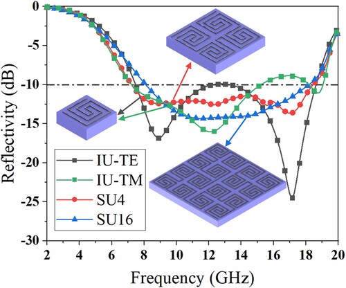
Table 1. Comparison of equivalent parameters of super unit with different number of units.
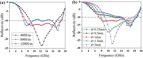
The main parameter of conductive fibre is conductivity. In the simulation, when the fibre conductivity (400 S/m, 800 S/m, 1200 S/m) is changed, (a) shows the influence of the conductivity of different conductive fibres on microwave absorption performance. It illustrated that appropriate conductivity is an important basis for wideband microwave absorption. Excessive resistance will affect impedance matching, while too small resistance will reduce the performance of electromagnetic wave loss. (b) shows the influence of the spacing d between the elements on the reflection coefficient. The spacing between cells is similar to the substrate distance of a capacitor, and the greater the spacing, the lower the equivalent capacitance value. Through the calculation of equivalent parameters, it is found that when d = 1.0 mm, C = 0.107 pF, while when d = 0.5 mm, C = 0.214 pF. The absence of equivalent capacitance will affect impedance matching and cause the resonant frequency points to drop to one [Citation31]. In addition, the absorption bandwidth first increases and then decreases, and the maximum absorption bandwidth is obtained when d = 1 mm.
Figure 7. Reflection coefficients of SU4 with different parameters: (a) fibre conductivity, (b) unit spacing d.
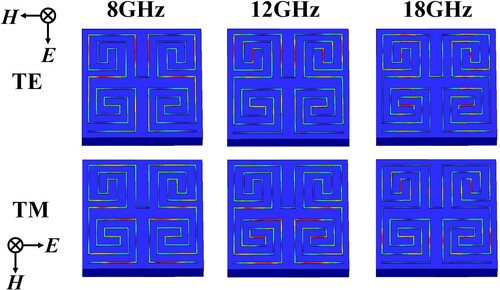
To further study the loss mechanism of the wave-absorbing metamaterial, shows the energy loss density diagram of SU4 under different resonant frequency points and polarisation modes. The energy loss is concentrated in the conductive pattern, and the part of the helical metamaterials parallel to the electric field concentrates the current, which realises the absorption of electromagnetic wave through the resistance loss of the structure. As the resonant frequency increases from 8 GHz to 18 GHz, the loss distribution concentrates from the edge to the centre of the element. This is related to the wavelength of the incident wave, and the shorter wavelength can be lost at multiple places in the unit. When electromagnetic waves with different polarisation directions are incident, the length of the conductive path parallel to the direction of the electric or magnetic field is not consistent in the upper and lower parts of the unit. Because the upper half of the unit possesses a longer conducting path parallel to the TE wave electric field, it generates a strong loss for the TE wave, while the lower part generates a loss for the TM wave. The combination of the two can reduce the polarisation sensitivity compared with IU arranged in the same direction.
Figure 8. Energy loss density diagram of SU4 under different resonant frequency points and polarisation modes.
4.2. Polarisation sensitivity and oblique incident stability
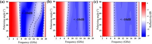
The polarisation reflectance spectra and oblique incidence reflectance spectra are used to analyse the wave-absorbing properties and stability of metamaterials. The reflectance images of IU, SU4 and SU16 at different polarisation angles are shown in . It demonstrates that the frequency band of the absorption microwave of IU shifts with the change of polarisation angle, showing polarisation sensitivity. However, SU4 exhibits a wideband absorption of −10 dB within 8–18.4 GHz under different polarisation angles. SU16 shows better polarisation stability, and the absorption bandwidth hardly changes. This reduction in polarisation sensitivity is in line with the loss principle shown in . The polarisation insensitivity of the conductive patterns arranged using space-filling curves proves the effectiveness of the unit arrangement method.
Figure 9. Effect of polarisation angle on absorption performance: (a) IU, (b) SU4, (c) SU16.
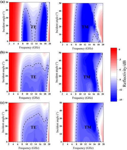
shows the reflectance simulation results of IU, SU4 and SU16 under the oblique incidence from 0° to 50° of TE and TM polarisation, respectively. Under the incident TE wave, the absorption frequency band of IU is 8–12 and 14–18 GHz, and the absorption intensity decreases with the increase of the incidence angle. However, under the incident of TM wave, the absorption band of IU covers 7.2–15.2 GHz, and with the increase of the incidence angle to 45°, the absorption band appears as a small blue shift. The TM mode has a more stable absorbing effect because changes in the incidence angle do not change the direction of the magnetic field and have less impact on metamaterial function. The absorption frequency band of SU4 under TM incident wave is 7.2–18.4 GHz. The absorption performance deteriorates with increasing incident angle, but SU4 can still maintain more than 80% absorption in TE polarised mode when the incident angle is less than 45°. SU4 under the TM polarisation can keep the reflectivity of less than −10 dB absorption even if up to 45°. The absorption effect of SU16 is very close to that of SU4, indicating the functional similarity of super units with more units. In general, it can maintain efficient absorption performance of electromagnetic waves in the range of 45° incidence angle. Compared with IU, the super unit designed based on space-filling curve improves the operating stability under oblique incidence.
Figure 10. Simulated reflectivity spectra at different incident angles. (a) TE and TM polarisation for IU, (b) TE and TM polarisation for SU4, (c) TE and TM polarisation for SU16.
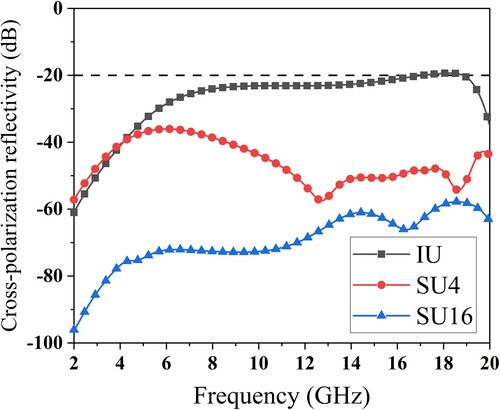
Asymmetric metal patterns show certain cross-polarisation conversion characteristics [Citation32], so it is necessary to evaluate the reflectivity of the cross polarisation of super units with different numbers of units. It can be seen from that IU shows the highest polarisation conversion rate, but it is also around −20 dB, which is equivalent to 1% of the electromagnetic wave polarisation conversion, proving that the reflectivity reduction of the metamaterial in this paper is basically based on absorption. SU4 and SU16 have lower polarisation conversion rates due to their higher structural symmetry.
Figure 11. Cross-polarisation reflectivity of the super unit with different numbers of units.
4.3. Scattering energy analysis
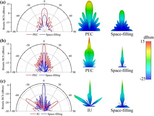
In order to measure the energy of electromagnetic waves scattered to the remaining directions at perpendicular incidence, the RCS of metamaterials with helical pattern is simulated and compared with PEC with equal area. It should be emphasised that since RCS simulation requires whole structures rather than units, the metamaterials used here are filled with 180 mm × 180 mm using larger super units generated by space-filling curves. (a,b) shows that the metamaterials generated by the space-filling curve have a large reduction in RCS in all directions compared with PEC when the electromagnetic wave is vertically incident at 8 and 18 GHz, which proves the electromagnetic wave absorption characteristics of the metamaterials. The 3D image of RCS illustrates the reduction effect of metamaterials more intuitively. (c) shows the IU with a single structure array appears to scatter the normal incident electromagnetic wave in the 60° direction, so that it exhibits a stronger scattering than the PEC. For the metamaterials arranged with space-filling curves for over-rotation combination, the scattering path is diversified [Citation33], thus reducing the strong peak of RCS, and the energy scattering is more symmetric.
Figure 12. Polar chart and 3D image of the bistatic RCS: (a) PEC surface and Space-filling metamaterials at 8 GHz, (b) PEC surface and Space-filling metamaterials at 18 GHz, (c) IU and Space-filling metamaterials at 18 GHz.
4.4. Experimental verification of absorber
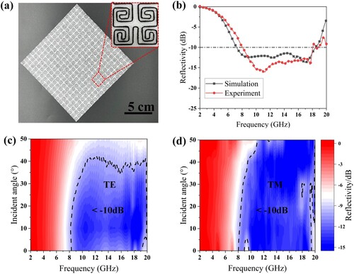
(a) shows the continuous conductive fibre-absorbing metamaterial prepared by multi-material 3D printing, which consists of a PLA substrate with carbon nanotube-coated dacron fibres composite printed on it. The magnification of the super unit shows that the preparation precision is high and consistent with the design pattern, which proves that the process stability of multi-materials hybrid 3D printing can form metamaterials. The reflectivity of the fabricated sample was measured to verify the broadband absorbing performance of the designed metamaterials experimentally. In (b), the experimental and simulated reflectivity test results are compared. It is displayed that the reflectivity of the fabricated sample is less than −10 dB or absorption of more than 90% is from 8 to 18.1 GHz, which is almost coincident with the simulation results. (c,d) shows the reflectivity test results of microwave-absorbing metamaterial with a helical pattern at different incidence angles. It is basically consistent with the trend of the simulation results. The actual prepared sample shows higher absorption amplitude and angular stability. It can basically maintain the broadband absorption when the incidence angle is 40°. The equivalent density is 1.12 g/cm3, and the design is based on the solid dielectric layer. If the dielectric layer design with porosity is adopted, the equivalent density can be further reduced while maintaining the bandwidth [Citation34].
Figure 13. (a) Sample of absorbing metamaterial; (b) comparison of measured and simulated reflectivity; measured reflectivity spectra of the proposed metamaterials at different incident angles of (c) TE polarisation and (d) TM polarisation.
In the absorptive frequency band, the absorption strength of the experimental test is improved, and the error is mainly caused by the deviation of manufacturing. (a) shows that although the printed path is the same as the designed path, the fibre traction causes the fibre to deviate from the original pattern, especially at the corner of the path. shows the fibre morphology on the metamaterial unit to further explain the error generation. (b) shows the torsion of the fibre at the corner makes the fibre width smaller, which makes the conductive area smaller. As shown in
Figure 14. (a) The unit of fabricated metamaterial; morphology of conductive fibre along the print path: (b) distortion of fibre, (c) particles dropped from the fibre coating and (d) fibre cross-section diagram.
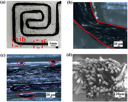
(c), the conductive coating of the continuous fibre has some particles falling off when it is extruded with the matrix, reducing the conductivity and causing the first resonant frequency point to move from the simulated 8.3 to 10.1 GHz. The gaps in the cured fibres can be used as resonant cavities to cross and interfere the incoming electromagnetic waves [Citation35]. The randomly appearing resonant cavity structure is composed of conductive fibres as the shell, and the PLA filled in it as the cavity to improve the absorption performance.
(d) shows a cross section of the coated fibre on the metamaterial, indicating that the matrix cannot penetrate effectively into the conductive coated fibre. Because there is a graphene coating on the surface of the fibre itself, it not only impedes the infiltration of the matrix but also ensures the stability of the conductivity for the wave-absorbing metamaterials.
summarises and compares the properties of the absorbing metamaterials based on the electric resonant loss. It is observed that the designed metamaterial has excellent bandwidth and thin thickness, and only one step of the forming process is needed to realise the resonant structure with integrated resistance loss.
Table 2. Comparison of properties and fabrication methods of absorbing metamaterials in the literatures.
5. Conclusion
In this work, a helical pattern microwave-absorbing metamaterial with a space-filled curve arrangement was fabricated using multi-materials hybrid 3D printing. It is proved that the conductive coating fibre can be equivalent to the uniform conductor to simulate the microwave absorption. The arrangement and connection mode of the unit can reduce the polarisation sensitivity, and its characteristics of one-stroke fabricating are more in line with the process requirements. Finally, the conductive fibre with resistive loss is used to achieve broadband absorption of 8–18 GHz, and the absorption rate of this band can also reach 80% (−8 dB) under the case of 40° oblique incidence. This work provides inspiration for the application of continuous fibres in wave-absorbing metamaterials. This process and design method of forming metamaterials has the advantages of rapid prototyping, lightweight and integrated fabricating with a medium layer and has great development potential.
Disclosure statement
No potential conflict of interest was reported by the author(s).
Data availability
The data that support the findings of this study are available from the corresponding author upon reasonable request.
References
- Schurig D, Mock JJ, Justice BJ, et al. Metamaterial electromagnetic cloak at microwave frequencies. Science. 2006;314(5801):977–980. doi:10.1126/science.1133628
- Huang Y, Song W-L, Wang C, et al. Multi-scale design of electromagnetic composite metamaterials for broadband microwave absorption. Compos Sci Technol. 2018;162:206–214. doi:10.1016/j.compscitech.2018.04.028
- Song W-L, Fan L-Z, Hou Z-L, et al. A wearable microwave absorption cloth. J Mater Chem C. 2017;5(9):2432–2441. doi:10.1039/C6TC05577J
- Gong P, Hao L, Li Y, et al. 3D-printed carbon fiber/polyamide-based flexible honeycomb structural absorber for multifunctional broadband microwave absorption. Carbon N Y. 2021;185:272–281. doi:10.1016/j.carbon.2021.09.014
- Bao S, Zhang M, Jiang Z, et al. Advances in microwave absorbing materials with broad-bandwidth response. Nano Res. 2023;16(8):11054–83. doi:10.1007/s12274-023-5654-6
- Landy NI, Sajuyigbe S, Mock JJ, et al. Perfect metamaterial absorber. Phys Rev Lett. 2008;100(20):207402), doi:10.1103/PhysRevLett.100.207402
- Wen Q-Y, Zhang H-W, Xie Y-S, et al. Dual band terahertz metamaterial absorber: design, fabrication, and characterization. Appl Phys Lett. 2009;95(24):241111, doi:10.1063/1.3276072
- Yin X, Long C, Li J, et al. Ultra-wideband microwave absorber by connecting multiple absorption bands of two different-sized hyperbolic metamaterial waveguide arrays. Sci Rep. 2015;5(1):15367, doi:10.1038/srep15367
- Nguyen TT, Lim S. Angle- and polarization-insensitive broadband metamaterial absorber using resistive fan-shaped resonators. Appl Phys Lett. 2018;112(2):021605, doi:10.1063/1.5004211
- Wu Y, Lin H, Xiong J, et al. A broadband metamaterial absorber design using characteristic modes analysis. J Appl Phys. 2021;129(13):134902. doi:10.1063/5.0043054
- Duan Y, Liang Q, Yang Z, et al. A wide-angle broadband electromagnetic absorbing metastructure using 3D printing technology. Mater Des. 2021;208:109900, doi:10.1016/j.matdes.2021.109900
- Tan R, Zhou F, Liu Y, et al. 3D printed propeller-like metamaterial for wide-angle and broadband microwave absorption. J. Mater Sci Technol. 2023;144:45–53. doi:10.1016/j.jmst.2022.10.012
- Zeng S, Feng W, Peng S, et al. Dual-functional SiOC ceramics coating modified carbon fibers with enhanced microwave absorption performance. RSC Adv. 2019;9(53):30685–30692. doi:10.1039/C9RA06166E
- Folgueras L de C, Nohara EL, Faez R, et al. Dielectric microwave absorbing material processed by impregnation of carbon fiber fabric with polyaniline. Mat Res. 2007;10(1):95–99. doi:10.1590/S1516-14392007000100020
- Yang Y, Wang J, Song C, et al. Electromagnetic shielding using flexible embroidery metamaterial absorbers: design, analysis and experiments. Mater Des. 2022;222:111079, doi:10.1016/j.matdes.2022.111079
- Lee S-E, Lee W-J, Oh K-S, et al. Broadband all fiber-reinforced composite radar absorbing structure integrated by inductive frequency selective carbon fiber fabric and carbon-nanotube-loaded glass fabrics. Carbon N Y. 2016;107:564–572. doi:10.1016/j.carbon.2016.06.005
- Lee S-E, Park K-Y, Oh K-S, et al. The use of carbon/dielectric fiber woven fabrics as filters for electromagnetic radiation. Carbon N Y. 2009;47(8):1896–1904.
- Yang J, Pang Y, Wang J, et al. Achieving broadband RCS reduction using carbon fiber connected composite via scattering mechanism. Compos Sci Technol. 2020;200:108410, doi:10.1016/j.compscitech.2020.108410
- Pang Y, Li Y, Wang J, et al. Carbon fiber assisted glass fabric composite materials for broadband radar cross section reduction. Compos Sci Technol. 2018;158:19–25. doi:10.1016/j.compscitech.2018.02.001
- Zuo W, Yang Y, He X, et al. An ultrawideband miniaturized metamaterial absorber in the ultrahigh-frequency range. Antennas Wirel Propag Lett. 2017;16:928–931. doi:10.1109/LAWP.2016.2614703
- Huang L, Duan Y, Dai X, et al. Bioinspired metamaterials: multibands electromagnetic wave adaptability and hydrophobic characteristics. Small. 2019;15(40):1902730, doi:10.1002/smll.201902730
- Tian X, Todoroki A, Liu T, et al. 3D printing of continuous fiber reinforced polymer composites: development, application, and prospective. Chinese J Mechan Eng: Addit Manufact Front. 2022;1(1):100016, doi:10.1016/j.cjmeam.2022.100016
- Khosravani MR, Frohn-Sörensen P, Reuter J, et al. Fracture studies of 3D-printed continuous glass fiber reinforced composites. Theor Appl Fract Mech. 2022;119:103317, doi:10.1016/j.tafmec.2022.103317
- Hao W, Liu Y, Zhou H, et al. Preparation and characterization of 3D printed continuous carbon fiber reinforced thermosetting composites. Polym Test. 2018;65:29–34. doi:10.1016/j.polymertesting.2017.11.004
- Khosravani MR, Soltani P, Weinberg K, et al. Structural integrity of adhesively bonded 3D-printed joints. Polym Test. 2021;100:107262, doi:10.1016/j.polymertesting.2021.107262
- Goh GD, Toh W, Yap YL, et al. Additively manufactured continuous carbon fiber-reinforced thermoplastic for topology optimized unmanned aerial vehicle structures. Compos Part B: Eng. 2021;216:108840, doi:10.1016/j.compositesb.2021.108840
- Gardner M. Mathematical Games. Scientific American. 1976;235(6):124-133. doi:10.1038/scientificamerican1276-124
- Hilbert D. Ueber die stetige Abbildung einer Line auf ein Flächenstück. Math Ann. 1891;38(3):459–460. doi:10.1007/BF01199431
- Petroff M, Appel J, Rostem K, et al. A 3D-printed broadband millimeter wave absorber. Rev Sci Instrum. 2019;90(2):024701, doi:10.1063/1.5050781
- Shang Y, Shen Z, Xiao S. On the design of single-layer circuit analog absorber using double-square-loop array. IEEE Trans Antennas Propagat. 2013;61(12):6022–6029. doi:10.1109/TAP.2013.2280836
- Zheng L, Niu L, Wang T, et al. Integrated lightweight gradient honeycomb metastructure with microwave absorption and mechanical properties: analysis, design, and verification. Compos Struct. 2023;305:116464, doi:10.1016/j.compstruct.2022.116464
- Gao X, Han X, Cao W-P, et al. Ultrawideband and high-efficiency linear polarization converter based on double V-shaped metasurface. IEEE Trans Antennas Propagat. 2015;63(8):3522–3530. doi:10.1109/TAP.2015.2434392
- Hou Y-C, Liao W-J, Tsai C-C, et al. Planar multilayer structure for broadband broad-angle RCS reduction. IEEE Trans Antennas Propagat. 2016;64(5):1859–1867. doi:10.1109/TAP.2016.2535164
- Yang Z, Liang Q, Duan Y, et al. A 3D-printed lightweight broadband electromagnetic absorbing metastructure with preserved high-temperature mechanical property. Compos Struct. 2021;274:114330, doi:10.1016/j.compstruct.2021.114330
- Huang M, Wang L, Pei K, et al. Multidimension-controllable synthesis of MOF-derived Co@N-doped carbon composite with magnetic-dielectric synergy toward strong microwave absorption. Small. 2020;16(14):2000158, doi:10.1002/smll.202000158
- Ding F, Cui Y, Ge X, et al. Ultra-broadband microwave metamaterial absorber. Appl Phys Lett. 2012;100(10):103506, doi:10.1063/1.3692178
- Li M, Muneer B, Yi Z, et al. A broadband compatible multispectral metamaterial absorber for visible, near-infrared, and microwave bands. Adv Opt Mater. 2018;6(9):1701238, doi:10.1002/adom.201701238
- Sheokand H, Ghosh S, Singh G, et al. Transparent broadband metamaterial absorber based on resistive films. J Appl Phys. 2017;122(10):105105, doi:10.1063/1.5001511