
ABSTRACT
This work proposes a rapid manufacturing technique for the conductive lines applied in flexible electronics, which is referred to as the ‘direct wire writing (DWW)’ technique. The fine metal wire is dragged out of the needle by adhesion, and attached to the stick-on substrate synchronously along design paths to form high-quality circuits. This technique overcomes the unstable performance of ink-based conductive lines fabricated by screen printing, spraying, 3D printing, etc., and avoids complex processes for stable metallic circuits mainly manufactured by the photolithography method, etc. Firstly, the forming mechanism of dominating the micro deformation behaviour (local-debonding, slip, warping) is clarified and analysed, which provides guidelines for fabricating in-plane wire patterns and 3D structural circuits rapidly and easily. Subsequently, some practical applications, including strain rosette, wearable sensor patch and light display are presented, showing the promising potential of the DWW technique in the ongoing exploration of flexible electronics.
GRAPHICAL ABSTRACT
1. Introduction
A large number of functional applications have been developed via various manufacturing techniques in recent years. For the conductive lines in devices, there are two main types of material systems: metal- and ink-base. Photolithography, evaporation or sputtering, etc. [Citation1–3] provide high-precision approaches to fabricating solid metallic circuits with stable performance but require expensive equipment, high-demanding consumables or complex processes affecting flexibility. Without considering the manufacturability and expensive material costs, liquid metals with good conductivity and deformability also offer promising application prospects in flexible electronics [Citation4]. Conventional screen/stencil printing, spraying, etc. [Citation5–7] use composite solvent- or polymer-based inks for the raw materials of conductive lines. The inks are usually composed of conductive fillers and polymer matrix and require eco-unfriendly pre- or post-treatment under different conditions (e.g. heating, photo-curing). Essentially, the conductivity of inks is usually much lower than that of metals [Citation8,Citation9]. For example, silver- and carbon-based inks are the two most commonly used printing materials in 3D printing, where the conductivity of carbon-based inks is 3 ∼ 4 orders of magnitude lower than the silver wire [Citation10], and the silver/solvent-based ink’s resistance is approximately twice that of bulk silver under ideal conditions [Citation11]. Accompanying the complicated conductivity mechanism (percolation, tunnelling and field emission conduction) of inks, environmental factors (e.g. temperature/humidity variations) and external loads (tension, compression, etc.) will inevitably affect the conductivity stability [Citation12–14]. Besides, It is difficult to achieve smooth line morphologies due to the intrinsic rheological properties and mixed material components of ink [Citation15,Citation16]. Minor defects resulting in performance degradation easily occur in the ink-based lines, which need time-consuming optimisation steps of material and process.
The 3D printing techniques (e.g. direct ink writing (DIW), digital light processing (DLP)) adopting composite inks surely simplify the manufacturing process compared to the above-mentioned techniques [Citation17–22]. It is convenient to obtain the designed circuits due to the flexibility and ease of use of 3D printing without requiring a mask or stencil, but the intrinsic properties of ink restrict the working performance of functional devices. How to combine the advantages of 3D printing techniques and high-stability metallic materials for convenient fabrication of conductive patterns is challenging, and worth further research. Herein, we propose the direct wire writing (DWW) technique by utilising the commonly used three-axis motion platform and supporting accessories for the DIW technique [Citation23–25], and replacing the ink extruded through the needle with the fine wire possessing good and stable conductivity. The traction force dragging the wire through the needle comes from the adhesion between the wire and the stick-on substrate, and then the wire is attached to the substrate surface effectively with the expected smooth patterns, without using any extruder or heating process. This forming process is different from the traditional wire embedding technology [Citation26–28] where a metal wire is actively extruded by a motor-actuated extruder, and inserted into the heated surface of a printed thermoplastic part by heating up and pushing the wire. Specifically, the surrounding plastic is melted by the heat and surrounds the applied wire, and then the wire and substrate are bonded together after cooling. Especially, unlike many existing processes (including the laser cutting process for the metal- or ink-based conductive lines [Citation29]), the low-cost DWW technique is capable of forming the controllable spatial spanning line structure, which can directly achieve the rapid insulation between the intersecting conductive lines in one step, without additional steps such as switching conductive/insulating materials backwards and forwards [Citation30].
The DWW technique is used not only for a series of in-plane and spatial conductive line patterns but also for more diverse functional applications in conjunction with other manufacturing processes. After the investigations about the local-debonding behaviour and mechanism for fine wire, combined with the DIW technique for the sensing units, the overall simplified processes can be applied to the high-precision strain sensor and new-type wearable sensor patch. Subsequently, a simple light display array is fabricated by inserting the commercial electronic components into the designed circuit, and an additional beneficial discussion about the complex spatial conductive line structure is carried out at the end. In brief, the DWW technique provides more technical choices for flexible electronics.
2. Methods
2.1. DWW forming process
Diverse conductive line designs, including the simple in-plane wire patterns, and the spatial spanning line structure with more functions, can be achieved by appropriately controlling the moving paths. As shown in (a), the schematic succinctly describes the forming process of the DWW technique. The key is that the traction force brought from the adhesion between the wire and stick-on substrate should overcome the received resistance force to the wire, in which the resistance mainly contains the friction force between the wire and needle inwall, and the mechanical force resulting in the bending or shape change of the wire along the moving paths. Here, the fine silver wire with good flexibility (Fig. S1 in Supplementary file) and conductivity is selected, and the stick-on polyimide (PI) film possessing good adhesion with silver wire (Figure S2) is chosen as the substrate after systematic trials. Note that the tapered needle is more suitable than the blunt tip type due to the smaller resistance force to the wire under the same inner diameter of the needle tip (Dneedle). Before the formal experiments, the wire is threaded through the needle manually, and then the syringe attached to the needle is clamped on the robotic arm of a three-axis motion platform. The silicone pad is used as the supporting substrate to fix the PI film (with the adhesive facing upward) via van der Waals force. A small segment of the wire outside the needle tip should be pressed and adhered to the PI film manually to provide the initial traction force. The inset shows the optical image near the needle tip, and it is seen that the silver wire is dragged out by the traction force and synchronously attached to the PI film. Note that the timer commands can be inserted into the target locations of the design paths before sending the printing programmes to the motion platform, to interrupt and resume the printing process at any time without relocation or cutting the wire. The comparison of morphologies between the wire and the ink-based (commercial silver, carbon paste) conductive lines is presented in Figure S3, where the intuitive feature is the much smoother surface profile for the wire without any additional processes such as etching or curing.
Figure 1. (a) Schematic diagram of the forming process for the DWW technique, where the inset shows that the silver wire is dragged out of the needle tip and is synchronously attached to the stick-on PI film. (b) Basic in-plane wire patterns (square, hexagon and spiral) written along the moving paths. (c) Corresponding moving path and a snapshot of the spatial spanning line structure. (d) Loop circuits containing basic in-plane shapes and spatial spanning structure, inspired by the NFC antenna.
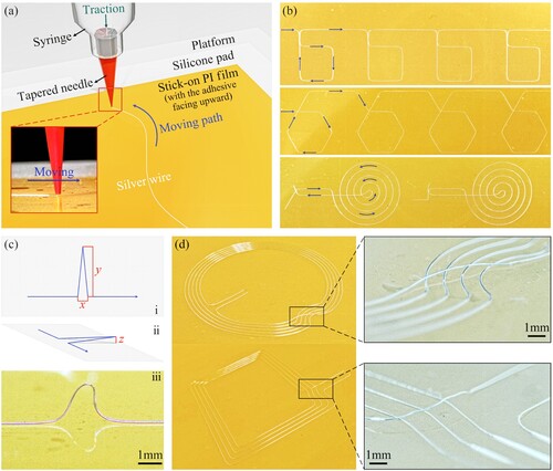
(b) presents some basic and typical in-plane wire patterns (square and hexagon: edge length is 10 mm; linear spiral: inner radius is 1 mm, outer radius is 10 mm, spacing is 2 mm) written along the programmed moving paths, and the arc corners of the polygon suggest the local-debonding and slip here. Note that the intersecting wires contact each other, where the wire is not coated with an insulator and there is no spacing between the wires. Considering that linear and curved shapes are the base of more complex patterns, it is necessary to summarise the corresponding manufacturing errors for the wire patterns with different corner angles or curve diameters, which is helpful to improve the final forming quality. The comparison of the manufacturing errors corresponding to the three groups of Dneedle: Dwire (the wire diameter) is presented in the corner tests ((a,b)), and the manufacturing error is defined as the minimum deviation between the formed wire corner and the design path divided by the adopted optical microscope vision width (namely ‘W’ in (c)). As shown in (d), the error overall decreases with the corner angle (5° ∼ 150°). It is found that the larger ratio of Dneedle to Dwire shows larger error, due to the oversized gap between the wire and the needle inwall, and the resulting non-ignorable misplacement of the wire in the needle tip. In the cases of the excessively large Dneedle: Dwire (1 mm: 80 μm), the local-debonding-induced error plus the large misplacement-induced error can cause a much larger overall error. Note that the fill areas among data curves denote the deviations caused by the different moving speeds (vspeed: 1 ∼ 9 mm/s), showing a relatively small effect compared with the ratio of Dneedle to Dwire. It means that vspeed can be adjusted to improve the printing efficiency with a relatively stable wire forming quality in a certain speed range. Specially, when printing straight wire (corner angle is 180°), the adhesion between the wire and the stick-on substrate will push the inner wire towards the tip side opposite to the moving direction, and restrict the wire misplacement in the needle tip. The cumulated adhesion along the wire also ensures the tight bonding between the wire and substrate. Thus, the straight line printed by the DWW technology has accurate forming quality, without debonding-slip and distortion.
Figure 2. Corner tests in the cases of (a) Dneedle: Dwire = 0.25 mm: 80 μm, and (b) Dneedle: Dwire = 0.25 mm: 20 μm. (c) Definition of manufacturing error. (d) Comparison of the manufacturing errors corresponding to different Dneedle and Dwire in the corner tests (angle: 5° ∼ 150°) under different moving speeds (vspeed: 1 ∼ 9 mm/s).
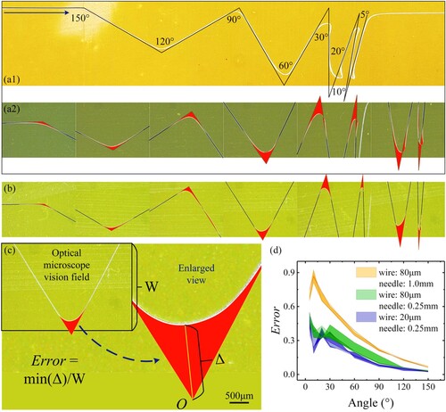
As shown in Figure S4,the error overall decreases with the curve diameter (2 ∼ 5 mm) and the larger Dneedle: Dwire tends to bring larger errors. The deviations caused by the vspeed (1 ∼ 9 mm/s) have a relatively large dispersity, especially for the small curves written by large needle tips. Moreover, it is feasible to write a tiny curve with a diameter of less than 100 μm when using a small Dneedle: Dwire (0.25 mm: 20 μm). Fig. S5 presents the manufacturing errors corresponding to the in-plane polygon patterns, as shown in (b), and the comparison between the two cases of Dwire = 20 μm or Dwire = 80 μm, showing the consistent changing trends with (d). Although the superfine wire with a small size (or large softness) has an advantage in forming tiny patterns, the excessively soft mechanical properties determine that debonding-warping from the substrate to form the spatial spanning structure is difficult for such wire. Additionally, it is unsuitable for further treatments such as transferring and connection used in diverse applications due to a lack of supporting strength. Thus, the needle and fine wire with the appropriate diameter (Dneedle = 0.25 mm, Dwire = 80 μm) are adopted in this work. Besides, the adhesion strength affects the printability and manufacturability of the DWW technology. The larger strength means the larger driving force to drag the wire out of the needle and then attach the wire onto the stick-on substrate smoothly. The large adhesion strength also reduces the debonding slip of written wire patterns to improve the overall manufacturing precision. However, relatively small adhesion strength can prompt the wire warping behaviour to form the out-of-plane wire spanning structure (for the insulation between the intersectant wires). The commercial stick-on PI film (adhesive thickness: ∼72 μm, supplier: Shenzhen Changdasheng Electronics Co., Ltd.) possessing the appropriate adhesion strength with silver wire is adopted in this work based on many trials. Collectively, the printing material properties, including the adhesion ability, modulus and geometry, should be considered in the DWW process according to the practical use.
To achieve more flexible and versatile functional patterns in conjunction with the simple in-plane shapes, we provide a novel method of fabricating the spatial spanning line structure easily and rapidly. As shown in (c), the corresponding moving path is shortly described as follows: The needle moves along the x-axis principal direction, then deviates towards the y-axis and slightly lifts along the z-axis simultaneously. Subsequently, the needle moves along the symmetrical path and returns to the original height in the z-axis simultaneously. The deviation from the principal direction results in the local debonding of the wire, and the restored moving direction and the needle height enable the re-adhesion between the wire and substrate. Additionally, the ‘triangle’ moving path reserves extra segments for the spatial spanning line structure, allowing other wires to pass below the ‘bridge’. Both ends of the span structure are stably adhered on the substrate to support the span middle hanging in the air steadily, and the support force also comes from the internal material stiffness. The base and height of the triangular moving path projected onto the plane are respectively defined as the x and y components, and the vertical distance between the apex and the base is the z component. The span value is the key variable, and the larger span value allows more wires to pass below the spatial spanning structure. Figure S6 summarises the spans corresponding to the different manufacturing parameters (x, y, z components and vspeed), and this work mainly studies the influence of the x, z component on the span value. It is found that the inappropriate (excessively small or large) x, y components will lead to the collapsed line structure. The span of the spatial structure overall increases with the x component (1 ∼ 4 mm) under the same other conditions, whereas the effects of the z component and vspeed are relatively small. After systematic experiments, the moderate parameters of x = 1 mm, y = 5 mm, z = 0.4 mm, v = 5 mm/s, and Hlifting (needle lifting height) = 0.3 mm are adopted for the following applications. Similarly, the span values corresponding to the rectangular moving path are presented in Fig. S7. The span overall increases with the x (0.5 ∼ 4 mm) or y (1 ∼ 9 mm) components under the same other conditions, whereas the influences of the z component and vspeed are relatively small. Compared to the rectangular moving path, the simple triangular moving path is more feasible for pursuing high manufacturing efficiency. The span contours corresponding to the varying x, z components, and the span trends changing with the y component and vspeed are shown in Figure S8, providing the reference of manufacturing parameters for different demands. The loop circuits, containing curves, straight lines and spanning structures, are displayed in (d), that is, the similar designs with NFC (near-field communication) antenna [Citation31–33] can be realised by the DWW technique, and it might be inspiring for many related intelligent applications.
2.2. DWW forming mechanism
To explain the forming mechanism and local-debonding-induced manufacturing error, the schematic illustration of the longitudinal section for the wire-adhesive-substrate sandwich structure along the moving path is presented in (a). Under the combined effects of the support and adhesion from the substrate and the drive from the needle inwall, the resulting upward bending deformation of the wire will cause weaker adhesion near the needle tip, compared to the adhesion region a little distance away. Take the corner tests as an example, the displacement of the needle tip can be decomposed into two movement components along the x- and y-axes. In the cases of the obtuse angle (90° ∼ 180°, (b)), the diagram of the top view shows that debonding along + x principal direction needs to overcome the stronger longitudinal reaction force not only from the tensile stiffness of wire but also from the cumulated adhesion along the wire. The weak bending stiffness of wire to resist the bending deformation, and the decreasing adhesion from the near to the far, determine the smaller resistance force when the debonding occurs along the y movement component. Figure S9 presents the related qualitative finite element (FE) simulations with the simplified but reasonable models, material properties and boundary conditions (geometry and material properties are listed in Tables S1–S3). In each simulation, the bottom edge of one end for the wire part is constrained in the degree of freedom (DOF) of the z-axis, and the surface of the other end is coupled to a reference point that a constant displacement load of 0.1 mm along different angles (90° ∼ 180°, realised by setting different movement components in x-, y-axis and constraining other DOFs) is applied to. The substrate part is set as a rigid body and constrains all DOFs. In this work, the commonly used cohesive zone model (CZM) [Citation34,Citation35] is adopted to analyse the debonding. The adhesive part is meshed using the cohesive element COH3D8, and other parts (wire and substrate) are meshed by C3D8R, where the approximate global mesh size is set as 0.1 mm. It is found that the reaction force at the reference point, namely the resistance force which needs to be overcome for the constant displacement of the wire end increases with angle. In other words, the local debonding and slip occur more easily for smaller corner angles. The reciprocal of the resistance force decreases with the angle, which shows a similar changing trend with that of the manufacturing error presented in (d), verifying the weaker strength induced by the y movement component in the obtuse moving path.
Figure 3. (a) Schematic illustration of the wire-adhesive-substrate sandwich structure along the moving path, where the adhesive interlayer contains weak and strong adhesion regions. (b) Schematic diagram of the top view for the obtuse corners (90° ∼ 180°), where the + x principal moving direction undergoes larger reaction force (namely, the debonding resistance force) compared to the y-axis moving direction. (c) Considerable peeling stress state in the acute corners (<90°) under the -x, y movement components, leading to the debonding of the weak adhesion region near the needle tip more easily.
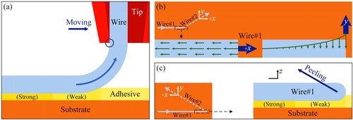
In the cases of the acute angle (<90°, (c)), the combination of the -x, y movement components will bring considerable peeling stress, and cause the debonding of the weak adhesion region more easily. It is understood that pulling the wire along/against the moving direction introduces the compressive/peeling stresses in the adhesive interlayer in the thickness direction (z-axis), which reinforces/weakens the adhesion region near the needle tip, respectively. Take the case with Dneedle: Dwire = 1 mm: 80 μm as an example, and the related observations are presented in Fig. S10. When the needle tip begins to write the other side of the small 5° corner, the formed side falls off the substrate and retreats into the needle until the debonding front enters the strong adhesion region. Then the wire dragged out of the needle approaches towards and sticks on the substrate, forming the local debonding-induced spatial warping in the small corner. Compared to the simple effect caused by the y movement component in obtuse corners, the complex forming process containing the retreat behaviour of wire determines the relatively large manufacturing error for acute corners. The same analytical methods can be introduced to explain the curve errors. A similar retreat occurs at small curves due to the weak total adhesion between the short curve segment and substrate, resulting in larger manufacturing error than that of the large curves. Thus, in addition to the accuracy improvement by optimising the manufacturing parameters, the further conceived methods are adding a rolling wheel or glue-dispensing nozzle near the needle tip, to strengthen the adhesion between the wire and substrate right after printing the wire segment. Based on the investigations about the debonding-slip behaviour and warping phenomenon of the in-plane wire patterns, the different spatial spanning structures can be realised in many applications via controlling manufacturing parameters.
3. Results and discussion
3.1. Rapid fabrication of strain sensor
The DWW technique can be used in various applications, especially the controllable spatial spanning structure significantly improves the forming speed of insulating intersecting conductive lines. Combined with the DIW technique, the rapid fabrication steps of the strain sensor are presented in (a). After writing the designed circuit, the strain rosette sensing layer (45°-type, sensor length is 5 mm) capable of measuring strains in three directions is printed on the PI film. The strain rosette has a common electrode and three independent ones, and the sensor electrodes are connected to the circuit at the setting position. In this section, the low-cost commercial carbon paste (CH-8(MOD2), Jujo Chemical) [Citation36,Citation37] is selected as the sensing material. After stirred and degassed at 2000 rpm for 3 min using a planetary mixer (ZYMC-180HV, Shenzhen ZYE Science & Technology Co., Ltd.), the obtained homogeneous mixture is transferred into a 5-cc syringe and then centrifuged at 3000 rpm for 5 min to remove bubbles using a high-speed centrifuge (TG1650-WS, Shanghai Lu Xiangyi Centrifuge Instrument Co., Ltd.). The printing parameters are optimised as follows: Dneedle (blunt tip needle) = 260 μm, Pair (air pressure) = 0.25 MPa, Hlifting = 0.15 mm and vspeed = 1.5 mm/s. After curing the sensing layer at 80°C for 3 h, the flowable two-part polydimethylsiloxane (PDMS; SYLGARD™ 184, Dow Chemical) is adequately mixed at a weight ratio of base/curing agent = 10: 1. Subsequently, the mixture is poured on the functional structures and cured at 65°C for 2 h for encapsulation and protection. Finally, cut off the surrounding redundant PI film and auxiliary circuit which is designed for writing row/column conductive lines smoothly. (b) presents the testing under uniaxial tensile loading, in which the sensor is mounted on a steel sheet by epoxy adhesive, and the speckle pattern for the digital image correlation (DIC) method detecting the surface strains are painted on the other sheet side. Then one end of the sheet is pulled at a quasi-static speed of 5 mm/min using an electronic universal testing machine (WDW-100kN, Jinan Sida Testing Technology Co., Ltd.), while a data logger (DAQ970A Data Acquisition System, Keysight Technologies) is used for recording the electric resistance changes of the sensor. It is found that the results measured by the sensor (gauge factor is 1.74 ± 0.076) and DIC method show a good agreement within the small strain range in three directions of 0°, 45° and 90° (Fig. S11 shows the resistance variation-strain curves of the strain rosette).
Figure 4. (a) Process steps of 45°-type strain rosette combined with the DWW and DIW techniques. (b) Comparison of testing results between the sensor and DIC method in three strain directions (0°, 45°, 90°) under uniaxial tensile loading. (c) Rapid fabrication of the large-area 5 × 5 sensor array by the same process steps, and (d) the moderate bending compliance of the array.
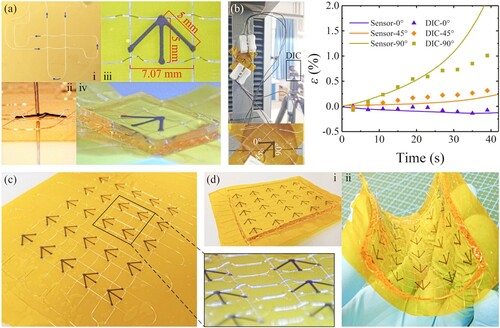
Moreover, the large-area sensor array can be fabricated by the same process steps easily and rapidly (5 × 5 array in (c)), showing the moderate capability of bending, as presented in (d). Note that the DWW/DIW techniques are capable of writing patterns on spatial curved surfaces indirectly by extracting 3D surfaces, mapping the 3D coordinates to 2D ones and then designing the moving paths (Fig. S12). Thus, a more complex spatial 3 × 2 sensor array attached to the undevelopable spherical surface is realised in Fig. S13, where the pre-cut designed substrate pattern by a cutting plotter, and the hollow structure near the wires and sensors are aimed to reinforce the array compliance for the convenience of mounting the array on a spatial surface. In brief, the above applications from the simple sensor unit to spatial sensor array show that the DWW technique possesses good feasibility and compatibility with widely-used manufacturing processes such as the DIW technique.
3.2. Flexible wearable sensor patch
Transferring the wire patterns to other resilient substrates provides more potential for flexible instruments. Take the sensor patch as an example, the complex serpentine (arc radius is 2 mm) conductive lines conforming to hand shape are written on PI film rapidly and then transferred on the temporary water-soluble tape by mechanical peeling method, as shown in Fig. S14, namely pressing the tape on the wire pattern, and peeling off the PI film slowly from one end to the other afterwards. The strength of the wire/tape side under normal stress conditions is usually larger than that of the wire/PI film side under shear stress conditions, which ensures the smooth transfer of the wire pattern. After mixing the two-part silicone Ecoflex (Ecoflex™ 00-20, Smooth-On) at a weight ratio of 1A: 1B adequately, the mixture is pourer on the tape attached with a wire pattern and cured at 85°C for 2 h. Then the tape is wetted with deionised water and peeled off using tweezers carefully to transfer the wire pattern to the resilient substrate. Note that the wire pattern is continuously written on the substrate in advance, and then manually cut to the desired length at the target locations. After removing the wires marked by the red lines, as shown in the diagram of (a), the ends of the red lines are put on the supporting PI pieces and applied with silver paste (8000H, Shenzhen Sunflower Electronic Material Co., Ltd.) to obtain the electrode pad after cured at 70°C for 30 min (marked in purple rectangular frame). The intersecting conductive lines are connected using the same steps and then reinforced by epoxy adhesive (DP125 Gray, 3M; curing condition: 71°C for 30 min), as marked in a green round frame. Subsequently, the designed serpentine (arc radius is 1 mm) strain sensors are printed on the target positions corresponding to knuckles, where the ends of the sensor are connected to the electrode pads, as shown in the illustration of (b). Finally, the resiliently stretchable circuit is connected to external wires, encapsulated by Ecoflex, and trimmed to obtain the sensor patch which can be mounted on the glove by medical polyurethane (PU) tape ((c)). The printing process of the sensor shown in (d) displays more details, where the enlarged view presents the electrode pads and the connection of intersecting lines. The stretchable carbon grease (846, MG Chemicals) [Citation38] capable of large deformation without the need for curing is selected as the sensing material, and the same material treatments as the carbon paste before printing. The optimised printing parameters: Dneedle (blunt tip needle) = 720 μm, Pair = 0.3 MPa, Hlifting = 0.3 mm, and vspeed = 5 mm/s.
Figure 5. Schematic diagrams of (a) the serpentine (arc radius is 2 mm) wire pattern and (b) the sensor layout in (c) the sensor patch, where the wires marked by red lines will be removed, followed by connecting the intersecting wires and putting the ends of the sensing layers on the electrode pads. (d) The printing process of the serpentine (arc radius is 1 mm) strain sensing layers at the knuckle positions. (e) Electric resistance changes of the sensor patch corresponding to different hand gestures.
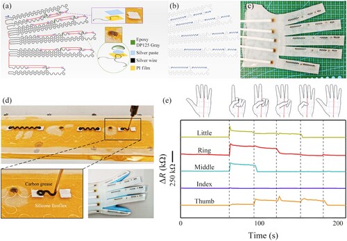
As shown in (e), extract the electric resistance changes of the sensor corresponding to the middle knuckle of each finger. The resistance of the sensor increases with the finger bending, causing the patch to respond to different hand gestures. Moreover, the good conductive stability of the wire/connection and the reversible dynamic response of the sensing layer under various strains are verified further, both of which ensure good performance for the sensor patch composed of the wire and sensor unit. Specifically, the tests about the serpentine (arc radius is 2 mm) wire/Ecoflex composite structure under linear cyclic loading at different strain levels of 5 ∼ 40% at a loading frequency of 0.5 Hz are presented in Figure S15. The two electrodes of the 0-Ohm resistor are connected to the middle-severed wire using the silver paste to form a current pathway, which is designed for testing the conductive stability of the silver paste/wire connections. It is found that the resistance of the intact wire without connections remains almost constant, and the relative resistance changes of the current pathway containing connections show only ∼7% increase within 400 cycles, verifying the good stability of resilient wire/Ecoflex. By contrast, the intact serpentine (arc radius is 2 mm) current pathways printed by commercial conductive inks are tested under uniaxial tensile loading at a speed of 1 mm/min, showing a relatively large resistance change of over 2% for silver paste, and over 50% for carbon paste at a small tensile strain of 6%, respectively (Figure S16). Additionally, the performance of the carbon grease-based serpentine (arc radius is 1 mm) sensor unit under linear cyclic loading at different strain levels of 5 ∼ 80% at a speed of 10 mm/min shows acceptable reversibility and stretchability (Figure S17). Collectively, the good feasibility of the DWW technique in conjunction with the transfer process is demonstrated by the flexible sensor patch, providing more possibilities for stretchable applications.
3.3. Flexible light display array
The wire written by the DWW technique can be connected with the commercial electronic components to realise other types of devices such as light displays. First, the wire pattern is transferred from the PI film to the temporary thermal-release tape by mechanical peeling method, as shown in Figure S14, then the two electrodes of LED (light-emitting diode) are connected to the middle-severed serpentine (arc radius is 2.5 mm) wire by silver paste (curing condition: 70°C for 30 min), and the translucent epoxy (DP125 Translucent, 3M; curing condition: 71°C for 30 min) is covered on the above structure for reinforcement, as shown in the diagram of (a). Subsequently, the mixed PDMS is poured on the tape and cured at 65°C for 2 h. After heating the tape until debonding, the released functional structure is transferred on the transparent PDMS substrate via the mechanical peeling method, followed by reinforcing the back of the connections between the wire and LED by epoxy. Finally, the simple flexible LED device capable of bending and stretching (tensile strain: 0 ∼ 36%) is obtained after encapsulation by PDMS ((b,c)). Replace the LED in the above device with the same 0603-package 0-Ohm resistor to test the conductive stability of the wire/PDMS composite structure under linear cyclic loading at a speed of 135 mm/min (Figure S18). It is found that the relative resistance changes of the current pathway show a maximum ∼3% decrease at the strain level of 5% within 1000 cycles and over 60% increase at the strain level of 10% within 60 cycles. The stretchability of the wire/PDMS is significantly smaller than that of the wire/Ecoflex, which is attributed to the hindrance to the free deformation of the wire by the stiffer PDMS (Young’s modulus: 2 MPa for PDMS, 55 kPa for Ecoflex) and the resulting plastic damage in the wire.
Figure 6. (a) Schematic diagram of the connections between the LED and the middle-severed serpentine (arc radius is 2.5 mm) wire via silver paste. Simple flexible LED device under (b) bending and (c) stretching (strain: 0 ∼ 36%). Complex light display array containing (d) the row/column wire pattern and (e) the red/blue LEDs arranged along characters ‘JN’, exhibiting the tolerant capability for bulging and bending. (f) Controllable luminescence of LED units inside character ‘N’ by turning on/off the corresponding circuit separately.
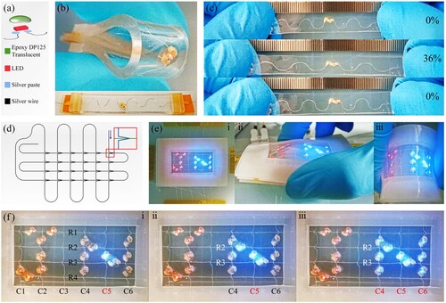
Furthermore, a more complex light display array, composed of the row/column wire pattern ((d)) and the red/blue LEDs arranged along characters ‘JN’, ia presented in (e), showing the tolerant capability for bulging and bending. Note that the triangular wires for forming spatial spanning structures in the column direction are placed below the straight wires of the row direction. The intersectant wires will contact due to the pressing operation during pattern transfer. After removing the external pressing loads, the spanning wire shape will recover to the suspended state by resilience or manually using tweezers. The encapsulated wire pattern by PDMS can further retain the wire shapes and the insulation between the intersectant wires. Surely the serpentine network (arc radius is 2 mm, Fig. S19) can be designed for more resilient application scenarios. As shown in (f), the LED units arranged along the characters ‘J’ and ‘N’ are inserted into the designed circuit array, where the LED units in each row/column circuit path are in series and the LED units in character ‘N’ can be turned on by manually connecting the current paths C5→R2R3→C4C6 one by one. The controllable luminescence of LED units indicates that the DWW-written conductive lines in conjunction with various electronic components may inspire many potential applications such as multi-module flexible circuits.
3.4. Preliminary exploration of complex spatial line structure
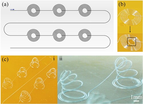
Except for the simple in-plane wire patterns and spatial spanning structure, a more complex spatial conductive line structure is inspired by the debonding-warping phenomenon resulting from the residual stress in small curves. As shown in (a), a series of in-plane linear spirals with radii ranging from 1.2 to 3 mm at a spacing of 0.3 mm are written on the PI film. The warping first occurs at the central smallest curve ((b)), and appropriate heating (e.g. 85°C) will accelerate the warping process from the inner to the outer curves. The resulting formed spatial helixes show a repeatable and stable shape ((c)), which is expected to be used in passive wireless sensors for strain and pressure sensing [Citation39]. The creative strategy is introduced to form complicated spatial structures by utilising the debonding-warping of simple in-plane patterns. Other complex spatial line structures can be realised by designing in-plane wire patterns indirectly or writing the spatial wire in supporting materials directly, which is worth researching further in future work.
Figure 7. (a) Schematic illustration of the in-plane linear spirals (radii: 1.2 ∼ 3 mm, spacing: 0.3 mm) on PI film. (b) Warping at the central smallest curve. (c) Spatial helixes formed by the accelerated warping under 85 °C, showing the repeatable and stable shape.
3.5. Comparison with the typical micro- and nano-3D printing technologies
In printing resolution, the minimum printed line width is ∼15 μm for aerosol jet printing [Citation40], ∼2 μm for inkjet printing [Citation41] and direct ink writing [Citation42], ∼6.7 μm for liquid substrate electric-field-driven (LS-EFD) jet printing [Citation43, Citation44], and ∼800 nm for localised electrochemical deposition micro additive manufacturing (LECD-µAM) [Citation45]; The current DWW technology can achieve a minimal curve shape diameter of ∼100 μm with a wire diameter of 20 μm, and a smaller wire size could be adopted according to the practical applications. In manufacturing capability, aerosol jet printing, inkjet printing and LS-EFD jet printing mainly focus on plane functional patterns, and direct ink writing and LECD-µAM can fabricate complex 3D porous and supporting structures. The current DWW technology can achieve diverse in-plane circuits and some out-of-plane structures including span wire and 3D helix. Accumulating layer by layer to build complex structures for more functional applications is our future research emphasis. In the working performance of printed circuits, for example, the silver paste used in LS-EFD jet printing has a significant resistance variation of ∼20% under 60% strain, whereas the silver wire with serpentine design fabricated by DWW technology shows almost constant resistance under 40% strain, due to the smooth electron flow in the bulk silver even under changing environmental factors or loads. Moreover, many high-value accessories, auxiliary tools and inks are also demanded for printing the high-resolution patterns in the listed micro- and nano-3D printing technologies. By contrast, the DWW technology adopted the easily available motion platform and metal wires is more cost-saving and user-friendly. Any eco-unfriendly material treatment of the metal wire is not needed and the formed patterns have smooth surface appearance.
Furthermore, more creative application could be achieved via the DWW technology by replacing the metal wire with functionalised filament as the printing material. For example, the electroluminescence or electrochromism filament can be chosen for a luminescent visualisation network or display screen in the human–machine interaction, wearable electronics or soft robotics. The removable sacrifice filament can be adopted for the microchannel or micropatterned substrate [Citation46] in sweat collection, drug delivery or cell support. The electrostriction, piezoelectricity and thermoelectricity filaments can be used for the artificial muscle or self-sensing actuator with energy generation and harvesting. Collectively, the above-mentioned applications and prospects of the DWW technique provide new insight into the body of knowledge of advanced devices [Citation47, Citation48].
4. Conclusion
The low-cost novel DWW technique is proposed to manufacture diverse high-quality in-plane wire patterns and out-of-plane spanning structures easily and rapidly, which overcomes the instability of ink-based conductive lines without complicated process steps. The effects on the forming quality under different manufacturing parameters by the local-debonding behaviour are further investigated by the related observations and FE simulations, which are attributed to the competition between the traction force and resistance force. Especially, the controllable spanning structure inspired by the debonding-slip phenomenon can realise the direct insulation of intersecting wires, which makes it possible to manufacture the conductive paths in one step. More importantly, the DWW technique in conjunction with other manufacturing processes such as the DIW technique and transfer method can realise high-complexity flexible devices. The high-precision strain rosette, new-type wearable sensor patch, light display array showing the potential of inserting the commercial electronic components into the written circuit, and beneficial discussion about the complex spatial wire structure demonstrate the high feasibility of the DWW technique which provides new avenues for flexible electronics.
Supplemental Material
Download PDF (4.3 MB)Disclosure statement
No potential conflict of interest was reported by the author(s).
Data availability statement
The authors confirm that the data supporting the findings of this study are available within the article and its supplementary materials.
Additional information
Funding
References
- Hua Q, Sun J, Liu H, et al. Skin-inspired highly stretchable and conformable matrix networks for multifunctional sensing. Nat Commun. 2018;9(1):244. doi:10.1038/s41467-017-02685-9
- Yang Y, Chiesura G, Plovie B, et al. Design and integration of flexible sensor matrix for in situ monitoring of polymer composites. ACS Sens. 2018;3(9):1698–1705. doi:10.1021/acssensors.8b00425
- Lanzara G, Salowitz N, Guo Z, et al. A spider-web-like highly expandable sensor network for multifunctional materials. Adv Mater. 2010;22(41):4643–4648. doi:10.1002/adma.201000661
- Dickey MD. Stretchable and soft electronics using liquid metals. Adv Mater. 2017;29(27):1606425. doi:10.1002/adma.201606425
- Hong H, Hu J, Moon K-S, et al. Rheological properties and screen printability of UV curable conductive ink for flexible and washable E-textiles. J Mater Sci Technol. 2021;67:145–155. doi:10.1016/j.jmst.2020.06.033
- Huang H, Chu X, Su H, et al. Massively manufactured paper-based all-solid-state flexible micro-supercapacitors with sprayable MXene conductive inks. J Power Sources. 2019;415:1–7. doi:10.1016/j.jpowsour.2019.01.044
- Hyun WJ, Secor EB, Hersam MC, et al. High-resolution patterning of graphene by screen printing with a silicon stencil for highly flexible printed electronics. Adv Mater. 2015;27(1):109–115. doi:10.1002/adma.201404133
- Kwon J, DelRe C, Kang P, et al. Conductive ink with circular life cycle for printed electronics. Adv Mater. 2022;34(30):2202177. doi:10.1002/adma.202202177
- Jia L, Zhou C, Sun W, et al. Water-based conductive ink for highly efficient electromagnetic interference shielding coating. Chem Eng J. 2020;384:123368. doi:10.1016/j.cej.2019.123368
- Chen H, Zhang Y, Ma Y, et al. Sand-milling exfoliation of structure controllable graphene for formulation of highly conductive and multifunctional graphene inks. Adv Mater Interfaces. 2021;8(1):2000888. doi:10.1002/admi.202000888
- Mahajan A, Frisbie CD, Francis LF. Optimization of aerosol jet printing for high-resolution, high-aspect ratio silver lines. ACS Appl Mater Interfaces. 2013;5(11):4856–4864. doi:10.1021/am400606y
- Nie X, Wang H, Zou J. Inkjet printing of silver citrate conductive ink on PET substrate. Appl Surf Sci. 2012;261:554–560. doi:10.1016/j.apsusc.2012.08.054
- Zhang R, Peng B, Yuan Y. Flexible printed humidity sensor based on poly(3,4-ethylenedioxythiophene)/reduced graphene oxide/Au nanoparticles with high performance. Compos Sci Technol. 2018;168:118–125. doi:10.1016/j.compscitech.2018.09.013
- Tian B, Yao W, Zeng P, et al. All-printed, low-cost, tunable sensing range strain sensors based on Ag nanodendrite conductive inks for wearable electronics. J Mater Chem C. 2019;7(4):809–818. doi:10.1039/C8TC04753G
- Li M, Yu P, Guo Z, et al. High-resolution and programmable line-morphologies of material-extrusion 3D printed self-leveling inks. Addit Manuf. 2023;71:103582. doi:10.1016/j.addma.2023.103582
- Hong H, Hu J, Yan X. Uv curable conductive Ink for the fabrication of textile-based conductive circuits and wearable UHF RFID tags. ACS Appl Mater Interfaces. 2019;11(30):27318–27326. doi:10.1021/acsami.9b06432
- Peng X, Kuang X, Roach DJ, et al. Integrating digital light processing with direct ink writing for hybrid 3D printing of functional structures and devices. Addit Manuf. 2021;40:101911. doi:10.1016/j.addma.2021.101911
- Zhou J, Yan H, Wang C, et al. 3D printing highly stretchable conductors for flexible electronics with low signal hysteresis. Virtual Phys Prototyp. 2022;17(1):19–32. doi:10.1080/17452759.2021.1980283
- Tang K, Ma H, Tian Y, et al. 3D printed hybrid-dimensional electrodes for flexible micro-supercapacitors with superior electrochemical behaviours. Virtual Phys Prototyp. 2020;15(sup1):511–519. doi:10.1080/17452759.2020.1842619
- Peng S, Thirunavukkarasu N, Chen J, et al. Vat photopolymerization 3D printing of transparent, mechanically robust, and self-healing polyurethane elastomers for tailored wearable sensors. Chem Eng J. 2023;463:142312. doi:10.1016/j.cej.2023.142312
- Peng S, Wang Z, Lin J, et al. Tailored and highly stretchable sensor prepared by crosslinking an enhanced 3D printed UV-curable sacrificial mold. Adv Funct Mater. 2021;31(10):2008729. doi:10.1002/adfm.202008729
- Peng S, Guo Q, Thirunavukkarasu N, et al. Tailoring of photocurable ionogel toward high resilience and low hysteresis 3D printed versatile porous flexible sensor. Chem Eng J. 2022;439:135593. doi:10.1016/j.cej.2022.135593
- Wang Z, Gao W, Zhang Q, et al. 3D-printed graphene/polydimethylsiloxane composites for stretchable and strain-insensitive temperature sensors. ACS Appl Mater Interfaces. 2019;11(1):1344–1352. doi:10.1021/acsami.8b16139
- Huang K, Dong S, Yang J, et al. Three-dimensional printing of a tunable graphene-based elastomer for strain sensors with ultrahigh sensitivity. Carbon N Y. 2019;143:63–72. doi:10.1016/j.carbon.2018.11.008
- Guo Z, Xu J, Chen Y, et al. High-sensitive and stretchable resistive strain gauges: parametric design and DIW fabrication. Compos Struct. 2019;223:110955. doi:10.1016/j.compstruct.2019.110955
- Kim C, Sullivan C, Hillstrom A, et al. Intermittent embedding of wire into 3D prints for wireless power transfer. Int J Precis Eng Manuf. 2021;22:919–931. doi:10.1007/s12541-021-00508-y
- Goh GL, Goh GD, Nguyen VP, et al. A 3D printing-enabled artificially innervated smart soft gripper with variable joint stiffness. Adv Mater Technol; 2023::2301426. doi:10.1002/admt.202301426
- Billah KMM, Coronel JL, Halbig MC, et al. Electrical and thermal characterization of 3D printed thermoplastic parts with embedded wires for high current-carrying applications. IEEE Access. 2019;7:18799–18810. doi:10.1109/ACCESS.2019.2895620
- Xu H, Zheng W, Wang Y, et al. Flexible tensile strain-pressure sensor with an off-axis deformation-insensitivity. Nano Energy. 2022;99:107384. doi:10.1016/j.nanoen.2022.107384
- Yu P, Qi L, Guo Z, et al. Arbitrary-shape-adaptable strain sensor array with optimized circuit layout via direct-ink-writing: scalable design and hierarchical printing. Mater Des. 2022;214:110388. doi:10.1016/j.matdes.2022.110388
- Scidà A, Haque S, Treossi E, et al. Application of graphene-based flexible antennas in consumer electronic devices. Mater Today. 2018;21(3):223–230. doi:10.1016/j.mattod.2018.01.007
- Xie Z, Avila R, Huang Y, et al. Flexible and stretchable antennas for biointegrated electronics. Adv Mater. 2020;32(15):1902767. doi:10.1002/adma.201902767
- Lee YK, Kim J, Kim Y, et al. Room temperature electrochemical sintering of Zn microparticles and its use in printable conducting inks for bioresorbable electronics. Adv Mater. 2017;29(38):1702665. doi:10.1002/adma.201702665
- Long H, Liang L, Wei Y. Failure characterization of solid structures based on an equivalence of cohesive zone model. Int J Solids Struct. 2019;163:194–210. doi:10.1016/j.ijsolstr.2019.01.008
- Xu W, Wei Y. Influence of adhesive thickness on local interface fracture and overall strength of metallic adhesive bonding structures. Int J Adhes Adhes. 2013;40:158–167. doi:10.1016/j.ijadhadh.2012.07.012
- Guo Z, Yu P, Liu Y, et al. High-precision resistance strain sensors of multilayer composite structure via direct ink writing: optimized layer flatness and interfacial strength. Compos Sci Technol. 2021;201:108530. doi:10.1016/j.compscitech.2020.108530
- Guo Z, Yu P, Liu Y, et al. Pre-fatigue enhancing both long-term stability and sensitivity of direct-ink-writing printed sensors. Int J Fatigue. 2023;166:107237. doi:10.1016/j.ijfatigue.2022.107237
- Muth JT, Vogt DM, Truby RL, et al. Embedded 3D printing of strain sensors within highly stretchable elastomers. Adv Mater. 2014;26(36):6307–6312. doi:10.1002/adma.201400334
- Wu Q, Zhu F, Wu Z, et al. Suspension printing of liquid metal in yield-stress fluid for resilient 3D constructs with electromagnetic functions. NPJ Flex Electron. 2022;6(1):50. doi:10.1038/s41528-022-00184-6
- Sinha AK, Goh GL, Yeong WY, et al. Ultra-low-cost, crosstalk-free, fast-responding, wide-sensing-range tactile fingertip sensor for smart gloves. Adv Mater Interfaces. 2022;9(21):2200621. doi:10.1002/admi.202200621
- Gao M, Li L, Song Y. Inkjet printing wearable electronic devices. J Mater Chem C. 2017;5(12):2971–2993. doi:10.1039/C7TC00038C
- Jiang P, Ji Z, Zhang X, et al. Recent advances in direct ink writing of electronic components and functional devices. Prog Addit Manuf. 2018;3:65–86. doi:10.1007/s40964-017-0035-x
- Li Z, Li H, Zhu X, et al. Directly printed embedded metal mesh for flexible transparent electrode via liquid substrate electric-field-driven jet. Adv Sci. 2022;9(14):2105331. doi:10.1002/advs.202105331
- Li H, Li Z, Li N, et al. 3D printed high performance silver mesh for transparent glass heaters through liquid sacrificial substrate electric-field-driven jet. Small. 2022;18(17):2107811. doi:10.1002/smll.202107811
- Ren W, Xu J, Lian Z, et al. Localized electrodeposition micro additive manufacturing of pure copper microstructures. Int J Extrem Manuf. 2022;4(1):015101), doi:10.1088/2631-7990/ac3963
- Seiti M, Ginestra PS, Ferraro RM, et al. Aerosol Jet® printing of poly(3,4-ethylenedioxythiophene): poly(styrenesulfonate) onto micropatterned substrates for neural cells in vitro stimulation. Int J Bioprint. 2021;8(1). doi:10.18063/ijb.v8i1.504
- Tan HW, Choong YYC, Kuo CN, et al. 3D printed electronics: processes, materials and future trends. Prog Mater Sci. 2022;127:100945. doi:10.1016/j.pmatsci.2022.100945
- Gao H, An J, Chua CK, et al. 3D printed optics and photonics: processes, materials and applications. Mater Today. 2023. doi:10.1016/j.mattod.2023.06.019