
 ?Mathematical formulae have been encoded as MathML and are displayed in this HTML version using MathJax in order to improve their display. Uncheck the box to turn MathJax off. This feature requires Javascript. Click on a formula to zoom.
ABSTRACT
In recent years, 3D printing has undergone a transformational journey – from prototyping technology, limited to laboratories, to a production method used in industry – becoming a powerful tool for creating functional objects. Despite this progress, 3D printing faces ongoing challenges related to defect detection and print quality control. We present an innovative, non-contact, fast and cheap microwave sensor for detecting defects in printed components, related to both mechanical errors and conductivity inhomogeneities. We discuss in detail the methodology of the microwave surface mapping technique and the results obtained for several samples printed with popular filaments. Tests show the ability to detect faults with millimetre precision. The simple design of the entire quality control module allows for easy integration with various types of 3D printers, from popular ones used by hobbyists to professional, highly specialised ones.
1. Introduction
3D printing is the process of constructing three-dimensional objects by adding individual layers of material. This technology has come a long way since its introduction, and it is now used in a wide range of applications, from simple DIY to the transportation industry and healthcare [Citation1,Citation2]. The ease of prototyping, the speed of model production, and the variety of available filaments (polymer, biodegradable, flexible, and even doped with metal powder) are the main advantages of Fused Deposition Modelling (FDM) technique. However, good print quality depends equally on the selected parameters of the printing process and filament, as well as the quality of the printer. Due to the relative novelty of FDM and the rapid development in filament diversity, prototyping 3D objects is still a process of trial and error, resulting in a huge amount of avoidable waste. As the popularity of 3D printing continues to rise, the environmental impact of these materials becomes increasingly crucial for sustainable innovation [Citation3]. Furthermore, the introduction of flexible or electrically conductive filaments provides new opportunities in the production of elements for many fields of technology, such as RF engineering [Citation4–7], telecommunication [Citation8,Citation9] or even military, but it also generates new challenges. Lack of ongoing control of advanced printing parameters (e.g. appropriate diversification of the speed of adding material in individual layer of the model being created) may cause many inconsistencies and differences in print density, leading to prototype defects, such as uneven distribution of stresses in the model or different values of electrical conductivity [Citation10,Citation11].
Currently, print quality is assessed primarily optically, with the naked eye or using web cameras, which allows for remote monitoring of the process. The growing market interest in automating various manufacturing processes has led to the development of several artificial intelligence-based quality monitoring tools that can also be integrated with FDM machines for printing control. However, optical sensors cannot determine the distribution of individual particles in a produced component, even when the component is assessed layer by layer. There are several advanced methods, such as integrated strain sensors [Citation12], X-ray tomography (used after printing) [Citation13], infrared thermography with camera [Citation14], ultrasound testing in post process evaluation [Citation15] and acoustic sensor capable of detecting common failures such as filament breakage or problems with filament extrusion [Citation16], which allow for an accurate assessment of the quality of the produced model. But none of them meets the technical and economic requirements necessary for use on an industrial scale. Consequently, increasing emphasis is being placed on the experimental evaluation of the mechanical properties of materials used in FDM, as well as on the application of Finite Element (FE) simulations with the use of advanced software like Abaqus FEA. These efforts aim to prevent failures in models potentially produced by FDM. Several studies show a correlation between these simulations and actual measurements, demonstrating the effectiveness of an accurate FE model. Such models are crucial for predicting the behaviour and strength of designed samples under various loading scenarios, material properties, and geometric conditions [Citation17]. FE modelling has become a valuable tool for the design and optimisation of FDM parts, aiding in applications such as lap joints [Citation18] and preventing common problems like delamination [Citation19]. However, it is important to note that discrepancies often exist between the predicted and observed behaviours of objects when tested for compressive strength, as highlighted in the literature [Citation20,Citation21].
One of the most promising methods for detecting material defects is the use of Radio Frequency (RF) sensors. The rapid development of RF engineering (most telecommunications devices communicate with each other using GHz signals) makes this technology affordable and reliable when used on a mass scale. An example of an RF sensor is the recently presented [Citation22,Citation23] Single Ring Resonator (SRR) probe, which can be used to map 2D materials and measure their relative dielectric permittivity. In this method, dielectric properties are measured with a probe almost in contact with the surface of the inspected element, which allows for mapping accuracy of several millimetres. A similar system for assessing surface quality was proposed in [Citation24]. The authors use a near-field imaging technique using reflected and transmitted signals between two waveguides to measure the dielectric parameters of the sample. However, both RF solutions mentioned here are laboratory prototypes and cannot be easily implemented by standard 3D printing users.
In the light of the above and due to the requirements to reduce the consumption of materials and the amount of waste, it seems necessary to develop a relatively simple method of examining the print quality layer by layer during the production of any parts. Therefore, we undertook work aimed at constructing a probe for ongoing print quality control, which should meet the following requirements: (i) detection of defects, contaminations and material inhomogeneities with at least millimetre precision, (ii) ease of implementation into any type of FDM 3D printer and (iii) low production cost.
As a result, we present a non-contact, fast and cheap microwave sensor for detecting material defects in 3D prints [Citation25]. The method was tested on elements made of filaments with different properties. Thus, we present the results of inspection of prints made of materials with various degrees of conductivity (copper/carbon-doped polymers) as well as non-conductive materials. We have chosen materials that are popular and easy to print, not requiring significant parameter adjustments during the printing process. We show that the proposed tool is effective both in detecting mechanical damage resulting from the filament spilling out of the extruder, its absence in the printout or the internal material stresses, as well as in assessing the uniformity of filament doping or the distribution of dopants after flowing from the extruder. This last ability is particularly important when using the latest generations of filaments which are often doped with materials such as carbon fibres or metallic powder to improve electrical conductivity. This doping often differs in local density, which can result in completely different material properties depending on the tested area.
The paper is organised as follows. In Section 2, we first present the near-field microwave imaging method used to control print quality and then we discuss the details of the measurement probe construction. In order for the probe to show reliable images of the layers added during printing, its optimal operating parameters must be determined. The preparation procedure is described in the last part of Section 2. The measurement results testing the probe’s ability to detect various types and origins of defects are presented in Section 3. The final remarks and perspectives are reported in Section 4.
2. Methodology
2.1. Near-field microwave imaging method
A near-field microwave imaging system shows the distribution of the dielectric properties of the test sample by measuring the diffuse field from multiple points of the object [Citation26]. In the present work, the open coaxial probe method in the reflection mode is used. The sample is placed on the open-end of transmit/receive probe interface. Due to the dielectric properties of the tested material, the sample causes a change in the load impedance and the incident wave is reflected. This kind of probe can be described in terms of the transmission line theory. (a) shows the most general model of the terminated transmission line circuit representing our probe, namely both generator and load present mismatched impedances to the transmission line one. The impedance of generator and load
is arbitrary and may be complex. The transmission line is assumed to be lossless with impedance
. The reflection coefficients of the load and the one seen looking into the generator are as follows:
(1)
(1) However, in the present case the generator is matched to the loaded line, so that
. We consider then only the reflection coefficient of the load. Although formally the above relation could be used to determine the dielectric characteristics of the sample, due to the practical problems associated with the measurements of voltages and currents at microwave frequencies, it is better to use a different approach. Namely, the use of ideas of incident, reflected and transmitted waves given in terms of the scattering matrix [Citation27]. The scattering matrix relates the voltage waves incident on the ports with the waves reflected from the ports and the scattering parameters can be measured directly with a vector network analyzer (VNA). For the N-port network, the scattering matrix has dimension
with elements type
being the transmission coefficients from port j to port i when all other ports are terminated in matched loads and elements type
being the reflection coefficients seen looking into port i when all other ports are terminated in matched loads. It turns out that in the case of our probe we only have the element
to measure which is exactly equal to the reflection coefficient of the load
((b)). Its value depends on the dielectric properties of the sample site where the reflection occurs due to the local modification of the load. Moreover, the value of
depends on the internal impedance of the probe and the impedance of the air gap between probe and sample, so finally:
(2)
(2) The vector network analyzer measures both magnitude and phase properties of the reflected wave. In (a) we present the photo of the test sample (a) and its images in the form of magnitude (b) and phase (c). It can be seen that for the purpose of detecting defects, the analysis of changes in the phase of the reflected wave is far more adequate, due to the fact that this parameter is the most affected by changes of a local environment of the probe. To increase the clarity of the visualisation and facilitate the automation of the scaling of the result in all figures, the phase changes were normalised in the range 0–1.
Figure 1. (a) Sensing system represented as a circuit from transmission line theory and the simulated (CST Studio) electric field distribution of the probe. stands for impedance of the material under test plus air gap between the end of the probe and the sample. (b) Schematical explanations of the S-matrix elements and their relationship to the reflection and transmission coefficients in a 2-port network.
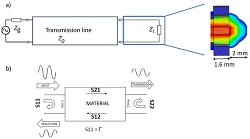
Figure 2. (a) Picture of the test sample (made from colorFabb Copperfill filament). (b) Magnitude and, (c) phase extracted from parameter.
2.2. Experimental setup
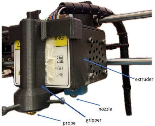
With a view to detecting material defects in real time, we built an experimental setup consisting of a coaxial probe connected by a coaxial cable to VNA. Our measurements were performed with two VNAs: MegiQ VNA0440 and PocketVNA, which were controlled by PC. The coaxial probe we used was made of a properly cut SMA connector [Citation28,Citation29] and was attached with a special gripper (printed from PLA) to the extruder of the 3D printer. In order to avoid interference with the construction of the original extruder, the gripper was attached to the outer part of the extruder at a distance of 5 cm from the nozzle (). A scheme of the system is presented in Figure S1 in Supplementary Materials. To enable the investigation of defects during the 3D printing process, we developed dedicated software that synchronises the VNA with the 3D printer. A single scan consists of multiple discrete measurements taken at the same distance above the sample. The scanning itself is automated and does not require human involvement, especially in terms of the scanning area and measurement time at each point of the printed element, which can vary from 0.05 to 0.5 s without affecting the quality of the measurement. The consequence of adding a defect sensor is the extension of the total time of the printing process. However, with the correct scanning settings, the total time for both printing and scanning should only be 10–15% longer than traditional printing. All measurement results presented in this paper were carried out in such a way that the scanning time was comparable to the time of printing a single layer. To visualise the scan results, an application with graphical user interface (GUI) has been developed. The application allowed to configure the scan and supported the scan itself synchronising work of VNA and 3D printer. Application was written in Python; GUI was prepared using pyQT and matplotlib was used to visualise the measurements. More information about application is available in Supplementary Materials.
Figure 3. Image of the probe attached to the extruder.
2.3. Preparation to measurements
In order to design and optimise the coaxial probe – sample system, simulations (CST Studio Suite) and corresponding real measurements were carried out. Coaxial probe dielectric spectroscopy is a well-established contact measurement technique [Citation24]. However, its use as a 3D printing quality controller during the printing process poses significant challenges. In particular, using it in contact mode is impractical for monitoring 3D prints due to factors such as the high temperature of freshly printed layers and the risk of compromising the structural integrity of the printed object. Therefore, adapting this method to non-contact work is necessary to avoid damaging the item during the printing process. In this context, the quality of the measurements at different distances between the probe and the sample should be checked in order to determine its optimal value. In the left column of , we present the simulated electric field distributions of the probe in the presence of a sample placed at three different distances from the probe, namely 0.1 mm (a), 0.5 mm (c) and 0.7 mm (e) for frequency f = 1.3 GHz, which was chosen arbitrarily and according to experiments does not have any advantage to other GHz frequencies. The right column of this figure shows the measurement results of fragments of uniformly printed PLA circular samples that correspond to the simulations presented in the left column, respectively. The boundary between the sample and the substrate blurs as the probe moves away from the tested area and it is evident that an efficient measurement can be made for a distance of the probe above the sample of up to 0.5 mm. Moreover, it is crucial to maintain a constant distance during measurements, because both dielectric properties of the space around the probe as well as a gap between the probe and sample affect the distribution of the electric field, and consequently parameter. Fortunately, in the 3D printing process, samples are created layer by layer, so if the sensor attached to the extruder is perpendicular to the table (bed), this problem can be easily avoided.
Figure 4. Left column – simulations of the electric field distribution (frequency 1.3 GHz) in the presence of a sample (PLA material with dielectric constant ) placed at the following distances from the probe: (a) 0.1 mm, (c) 0.5 mm, (e) 0.7 mm. Right column – (b, d, f) phase change measurements (normalised to background) corresponding to the presented simulations, respectively. Printing parameters: speed 60 mm/s, 100% infill, nozzle diameter 0.4 mm.
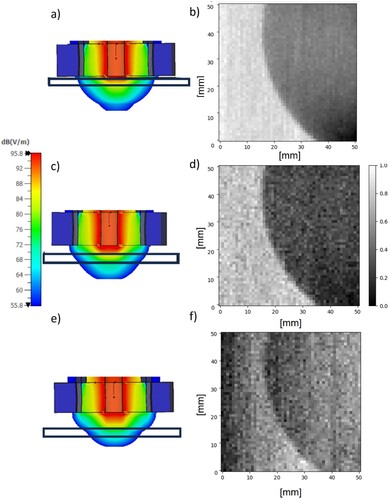
For the current experiment, all measurements were taken at a height of 0.1 mm above the samples. This distance between the sensor and the sample can be easily aligned in most of 3D printers, which are available on the market. The precision of controlling the height varies depending on the technology and model of used devices. While some high-end industrial 3D printers can achieve even a precision of tens of micrometres, most desktop 3D printers typically operate at a level measured in fractions of a millimetre. The achievable level of controlling of position of extruder and bed is influenced by many factors such as the printer's design, print settings, and the quality of the materials used by the manufacturer. For our experiments, we used Anycubic i3 Mega, a 3D printer without advanced technology for determining the height of the extruder above the bed. Consequently, manual calibration was necessary using the basic ‘sheet of paper’ technique. The probe's position was adjusted simultaneously with the nozzle to ensure that both were set at the same height. It was also found that small differences (up to 0.3 mm) in the height of the probe and nozzle do not affect the quality of the results from the probed surface, provided that the height is maintained constant throughout the scanning time.
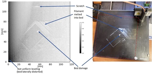
The first scans were made over an empty bed, which in one of our printers was damaged by a filament embedded in it. As can be seen in , the exact location of the bed defects is possible thanks to the measurement of parameter . In addition, it can be observed that the bed is not perpendicular to the extruder (the screw supporting the lower right corner of the bed had a lower height than the other 3). This part of the measurement preparation is essential for the correct interpretation of the results. Since it is very important to maintain a constant height of the probe above the sample, eliminating any disturbances in this area at this stage (e. g. by taking them into account when subtracting the background or by properly levelling the bed) will facilitate further data processing.
Figure 5. Image of the bed in the form of phase changes obtained by scanning with the probe placed at a distance 0.1 mm from it.
Furthermore, analysis of the parameter allowed us to distinguish noise patterns occurring in both magnitude and phase images, which originates from the magnitude change and phase shift of the bending coaxial cable during the scanning process. This noise can be easily eliminated by measuring the
parameter at each position during calibration before measurements or after performing the experiment, and then using this additional result to filter the measured data.
After properly levelling the bed, our setup is ready for measurements. For the purpose of test measurements, some popular filaments were chosen, namely: PLA (different colours), BioWood, PETG, carbon-doped filaments (Protopasta Conductive PLA, Recreus Conductive Filaflex Black TPU and two experimentally manufactured PETG materials doped with carbon fibres), PLA doped with metallic powder (colorFabb Copperfill) and BASF Ultrafuse 316L infused with steel.
All samples were designed with the use of Fusion 360 software and then exported as.stl files to Ultimaker Cura – software that allows to generate layer-by-layer interpretable file for 3D printer (g-Code file) and prepared on an AnyCubic i3 Mega printer equipped with a brass nozzle with a diameter of 0.4 mm. For all discussed samples following slicer settings were used:
Layer: Height: 0.2 mm; Initial Layer Height: 0.3 mm; Line Width: 0.4 mm.
Wall: Thickness: 0.8 mm; Line count: 2; Horizontal Expansion: 0.
Bottom and Top layers: 4; Disabled ironing.
Infill Pattern: grid; Overlap percentage: 10%.
Build plate adhesion: skirt.
Fan: Initial speed 0%; Regular speed: 100% from layer 2.
The following printing conditions were selected to produce the individual samples:
PLA and BioWood (by company ROSA 3D): Nozzle temperature 210°C, bed temperature 60°C, printing speed 50
, infill 100%.
PETG (by company ROSA 3D): Nozzle temperature 225°C, bed temperature 70°C, printing speed 50
Protopasta PLA Conductive: Nozzle temperature 220°C, bed temperature 60°C, printing speed 60
Recreus Conductive Filaflex Black TPU: Nozzle temperature 240°C, bed temperature 70°C, printing speed 50
colorFabb Copperfill: Nozzle temperature 220°C, bed temperature 60°C, printing speed 50
BASF Ultrafuse 316L: Nozzle temperature 230°C, bed temperature 90°C, printing speed 50
3. Results and discussion
According to the simulations carried out before the experiments all samples should be detected by the probe. Due to the higher value of permittivity materials doped with metal powder or carbon fibres should cause greater change in measured phase than homogeneous nonconductive materials like PLA and PETG. In (a) we present six samples printed from different materials, and (b) shows the results of measurements in the form of changes in the phase of the reflected signal.
Figure 6. (a) Photography of 6 samples: A – PLA by ROSA 3D, B – experimentally manufactured PETG with 15% carbon fibres addition, C – experimentally manufactured PETG with 10% carbon fibres addition, D – PETG by ROSA 3D, E – ColorFabb Copperfill, F – BioWOOD by Rosa 3D, (b) change in the phase of the measured signal (Inset shows the phase image of sample F after filtering out the noise), (c) defects which were detected by sensor: B1, E3, F4 – filament shrinking in the corner of the samples, C2 – unwanted change of the infill that caused tension in a sample, (d) Optical microscope image of the surface of sample E with visible uneven distribution of metal powder.
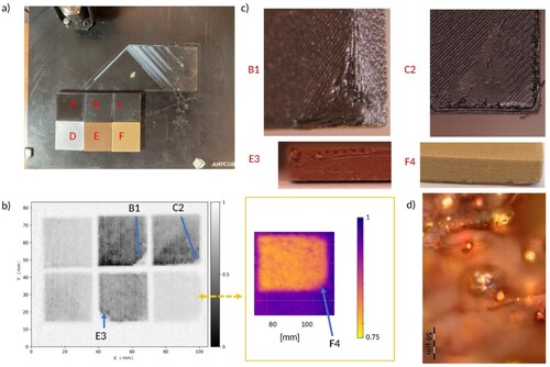
As expected, the sensor detected all uniformly printed samples ((b)) indicating inhomogeneities B1, C2 and E3. As expected, the maximum phase change, 16.3 degrees compared to the background, was recorded for sample B, which has the highest dielectric constant of = 8.1 ± 0.4. Samples made of pure polymers (A, D, F), characterised by a low dielectric constant (<4), showed a smaller change in the phase of the reflected signal compared to samples made of doped polymers (B, C, E). However, even in the case of samples A, D and F, the difference between them is noticeable and allows to distinguish the tested elements and to notice potential defects. As an example, let us analyse the results for sample F, produced from BioWOOD by Rosa 3D (
= 2.6), which induced the smallest phase change from all measured samples. The inset in (b) shows an image of this sample after applying a simple high-pass filter to phase change values from 0.75 to 1. It can be seen that one can easily distinguish it from the background. The average phase change for the background is 0.03 with a standard deviation of 0.0015, while for the uniformly printed F sample, the average phase change is 0.18 with a standard deviation of 0.03. This shows that even non-conductive materials with low dielectric constants can be detected and analysed using the microwave we describe. It is therefore expected that it will be possible to effectively control the print quality of elements made of materials commonly used in FDM printing such as PLA, ABS or PET with dielectric constants (for 100% infill) usually around
= 3 at GHz frequencies[Citation30].
Samples with carbon/copper addition (B, C, E) turned out to be more heterogeneous than A, D, and F. This can be a result of several factors, such as the uneven distribution of conductive additives [Citation31–33] or impaired filament extrusion due to nozzle clogging by the dopants [Citation34–36]. In case of uneven distribution of conductive powder within a sample, several methods can be used to examine it. For instance, X-ray tomography can provide direct imaging. Additionally, uneven distribution can be indirectly tested by measuring surface resistivity, or visually confirmed through optical microscopy [Citation37], as demonstrated for sample E in (d). This finding agrees with the manufacturer’s claim in the technical datasheet for ColorFabb Copperfill, which states that although the filament is densely infused with copper powder (density of 3.9 , approximately three times that of typical pure PLA), it remains non-conductive, even after potential debonding and sintering processes.
In microwave measurements, non-uniform distribution of conductive powder or carbon black, translates directly into increased standard deviation of the measured average phase change within the sample. On the other hand, defects are distinguished based on measured phase changes that fall within the range of background values.
The exact origin of heterogeneities in samples B and C remains unclear due to limited information on the material's manufacturing process. The most likely cause of the visible defects and inhomogeneities in these samples is problems with filament extrusion. These two non-commercial filaments, provided by a local manufacturer, were part of an experimental trial to create an Electrostatic Discharge (ESD) material. However, this goal was not achieved, which is confirmed by research conducted in our laboratory.
Let us note that the defects detected by the probe in are quite large and also visible directly on the samples. However, these samples were suitable for preliminary testing of the sensitivity of the proposed microwave system, especially with respect to non-conductive samples (see defect F4 in the inset of (b)) and those made of popular materials used in FDM modelling. What is important is that the results obtained are characterised by four times better spatial resolution than that presented in other research devoted to RF defect sensing [Citation22] and three times better than the sensor presented in [Citation24].
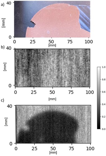
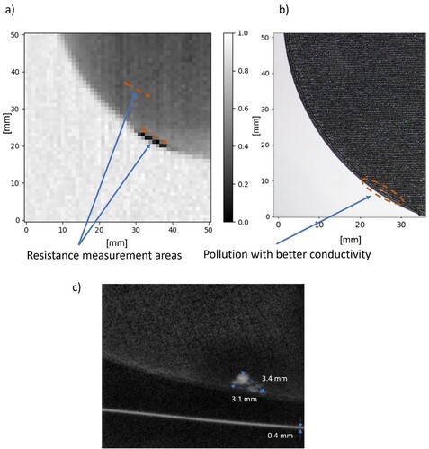
However, one of the greatest advantages of microwave measurements, compared to the optical control of printing, is the ability to obtain information about defects that are not visible at first glance. As an example, we examined the sample that was printed in another lab. In (a), it is easy to notice an area of distinctive intensity that corresponds to the fragment of the sample marked in its photograph ((b)). Note that the contamination (with dimensions 1.2 mm by 2.4 mm) visible on the sample is smaller in size than that detected by the microwave sensor. This result may indicate that the contamination is also present in the internal layers of the sample and is characterised by different dielectric properties. The simplest way to confirm this hypothesis is to examine the electric conductivity in two areas marked with line segments in (a). The resistance in the contaminated part of the sample was measured to 170 ohms lower, which means that the contamination material is more conductive than the rest of the sample. Indeed, a more conductive filament namely Electrifi Conductive Filament was used for the previous print and undoubtedly some of this material remained in the nozzle. To verify this observation, the sample was subjected to X-ray examination with the following parameters: 50–70 kV and 1.4–5 mAs [Citation38] ((c)). X-ray imaging confirmed that the size of contamination with the more conductive material had exceeded the area visible on the surface ((b)), now extending to approximately 3.1 mm compared to 2.4 mm. These results suggest that microwave sensing offers distinct advantages over visual inspection methods such as camera imaging [Citation39] and infrared thermography [Citation15]. Although these methods claim even submillimetre precision, they often fail to detect internal defects within samples, highlighting the superior diagnostic capabilities of microwave sensing for such applications. However, it should be noted that the contamination visible in the X-ray image has a different shape than that detected by our probe. This is related to the depth of penetration of microwave radiation, which in this case was of the order of 0.4 mm. Some of the contamination not visible in (a) is located in the sample layer beyond the reach of the probe and to detect it, an inspection should be carried out during the printing process as in the case of sample shown in .
Figure 7. Sample made from Protopasta PLA conductive: (a) change in the phase of the measured signal, (b) photo of the sample, (c) X-ray of the sample with marked region of contamination (3.4 mm) and steel wire with diameter 0.4 mm placed near the sample as a measurement reference. Parameters used for X-ray imaging: 70 kV and 2 mAs.
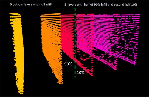
In the next step, we examined the probe’s sensitivity to detecting PLA samples with different infill densities. For this purpose, a set of samples (made from the green and blue PLA made by ROSA3D) was prepared, differing only in the filling density (). Moreover, each sample was designed using the Ultlimaker Cura grid pattern to additionally combine parts with different infill densities. By narrowing the infill gap between the two halves of the sample, it is possible to estimate the minimal difference still noticeable by sensor. All samples presented in were printed under the following conditions: nozzle temperature 210 °C, bed temperature 60°C, printing speed 50 mm/s. It has been found that changes of infill density of 20% between the two halves are easily detectable ((b)). Moreover, even in a sample with sparse filling (30% – (a)), internal walls with a thickness of 0.4 mm can be observed. However, due to the submillimetre size of the walls, distinguishing their exact locations and potential defects in this part of the sample is challenging. Nevertheless, after applying a high-pass filter (similar to that shown in (b)), it is easier to identify defects in both samples ((a,b)) as well as the inner walls of the 40% filled sample ((b)). In the case of a sample made of PLA with 30% infill ((a)) the use of such a simple filter did not improve the quality of the phase image and further analysis is necessary. For this purpose, a sample with two halves with 90% and 10% filling was used ((c)). The measurements were carried out in such a way that scanning took place every three printed layers of the sample. The scanning speed has been adjusted to the time needed to print one additional layer. The first 6 bottom layers were printed with 100% infill to avoid stress in the sample and the remaining 9 layers were printed with 10% and 90% infill in the respective halves of the sample. As expected, the phase changes measured on the surface in the 10% filled part are within the range of background values. The use of advanced filters and cutting out the background (details in Supplementary Materials) allows not only to isolate this part of the sample from the background but also to visualise its 3D structure ( and Figure S2 in Supplementary Materials).
Figure 8. A set of samples made of PLA (photos in the left column), the corresponding phase images (middle column) obtained using our microwave probe and their filtered counterparts (right column). All samples were prepared with the same slicer settings except for the filling density: (a) 70% to 30%, (b) 60% to 40%, (c) 90% to 10%.
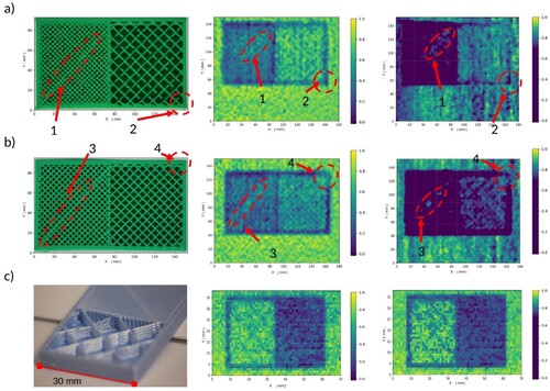
Figure 9. 3D structure of the sample shown in (c) after filtering the data according to the procedure described in the Supplementary Materials.
lists the most probable causes of all defects marked from 1 to 4, according to their numbering in . These defects occurred during the printing process, and their effective detection is crucial in all cases where perfect uniformity of the printed elements is required.
Table 1. The most probable causes of all defects found in the samples from .
Moreover, by using contact mode between the test sample and the coaxial probe, measurements of the dielectric constant of the printed element can be carried out. There are various methods for converting the measured reflection coefficient into the electrical permittivity of the sample [Citation40]. It is worth noting that in the majority of modern VNAs, this operation is automatically performed by embedded software. However, in the present case, the determination of the dielectric constants was based on the method described in [Citation19] where the dielectric properties of liquid samples were measured using a similar SMA coaxial probe. As reference samples we used two liquids: distilled water and ethanol, and two solid materials: PTFE (Teflon) and polystyrene. Measurements were carried out at a temperature of 24 degrees Celsius and a humidity of 39% using PocketVNA calibrated with the True-Reflect-Line technique (1001 points for the 1–4 GHz band). The results, including surface resistivity values measured by the concentric ring probe technique, are summarised in . The method used here to measure surface resistivity uses a probe () with two electrodes, where the current () flows on the sample surface from electrode A to B. To prevent measurement disturbances caused by the current penetrating the bulk (
), an additional electrode C is used to collecting electrons that do not originate from the sample surface. Surface resistance
can be calculated from the ohm’s law and then can be converted to surface resistivity according to the formula
, where
and
are the radii of inner and outer electrodes.
Figure 10. Concentric probe technique: photo of the probe and scheme of current distribution in the system. – surface current,
– current coming through the bulk, A – outer electrode, B – inner electrode, C – guard electrode.
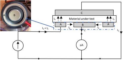
Table 2. The dielectric constant and surface resistivity of some samples printed with different filaments.
As expected, the measured dielectric constant of PLA is consistent with the values reported in the literature [Citation40,Citation41]. Furthermore, it is worth noting that the filament with the addition of copper powder has only a slightly higher dielectric constant than homogeneous PLA and is non-conductive. This result is in line with expectations because, according to the manufacturer, the addition of copper only has a hardening function. In this case, the conductive additive has no effect on increasing the conductivity, probably due to the lack of connection between the copper particles distributed chaotically throughout the sample.
Two samples made of carbon-doped filaments were found to be conductive. The most conductive sample tested was TPU infused with carbon black and carbon fibres. According to information from the producers, this flexible filament was designed for the production of wearable electronics and in light of the results obtained here, such use seems to be quite justified. In the case of PLA doped with carbon black, the dielectric constant values reported by different research teams differ significantly [Citation5,Citation9] even for material from the same producer. This is because these properties are significantly influenced by printing speed, infill percentage, layer height, and nozzle quality. However, it should be emphasised that the measured value of dielectric constant ϵ = (18.11 ± 0.87) falls within the range of values found in the literature.
Interestingly, measurements performed on a sample made of a filament saturated with steel powder show a much higher dielectric permittivity compared to a classic homogenous polymer filament, but much lower compared to filaments with carbon. On the other hand, a detailed analysis of the results indicates dense packing of steel particles, which after appropriate heat treatment have a chance to connect. This should result in a highly conductive sample, which is consistent with manufacturer’s information that debonding and sintering should result in conductivity at the level of pure steel.
4. Final remarks
Despite extensive research on non-destructive testing methods in material engineering, there is still a need for innovative quality control approaches adapted to FDM 3D printing. The paper presents a simple and cheap microwave system for detecting millimetre size defects. Compared to existing approaches, the presented method makes it possible to detect not only defects related to extrusion problems, but also imperfections in the doping of materials used for 3D printing. This last skill is very important when printing elements with strictly required dielectric properties.
The developed software and hardware were tested on three commercially available inexpensive printers: Prusa i3, Anycubic i3 Mega and Anycubic Kobra, giving results similar both qualitatively and quantitatively. It can therefore be expected that the tool proposed here can also be effectively used in 3D printers of other types and brands. Moreover, Vector Network Analyzers used to generate and analyse the signal are easily available to all professionals but also affordable (due to the relatively low price) for many 3D printer hobbyists. The only challenge when using this tool is the need to maintain a constant distance between the probe and the sample during the entire printing process.
The ability to evaluate local material properties in real time can serve as a near-instantaneous quality control method, particularly with respect to permittivity characteristics. The non-contact and non-destructive features of the dielectric imaging technique also create potential applications beyond the scope discussed here. For example, it could be used in various additive manufacturing processes to monitor aspects such as material deposition, hardening or detecting defects in softer materials. Additionally, this technique could play a key role in mapping the property changes that occur when combining different materials.
In the near future it is planned to modify the algorithm in such a way as to continuously compare the data collected by our sensor with information from CAD files which will enable early detection of errors in relation to the design. During this step, specific values for defects and nonuniform infill detection will be investigated with respect to the most popular FDM materials like PLA, PET and ABS with different printing speeds. The problem of detecting defects in prints of more complex shapes and/or different fill densities will be the subject of a separate paper.
Supplemental Material
Download MS Word (176.7 KB)Disclosure statement
No potential conflict of interest was reported by the author(s).
Data availability statement
The data that support the findings of this study are openly available in Figshare: https://figshare.com/projects/Non-contact_microwave_sensor_for_FDM_3D_printing_quality_control/199747.
Additional information
Funding
References
- Paul GM, Rezaienia A, Wen P, et al. Medical applications for 3D printing: recent developments. Mo Med. 2018;115(1):75–81.
- Teweldebrhan BT, Maghelal P, Galadari A. Impact of 3D printing on car shipping supply chain logistics in the Middle East. Asian J Shipp Logist. Sep. 2022;38(3):181–196. doi:10.1016/j.ajsl.2022.06.003
- Rodríguez-Hernández AG, Chiodoni A, Bocchini S, et al. 3D printer waste, a new source of nanoplastic pollutants. Environ Pollut. Dec. 2020;267:115609. doi:10.1016/j.envpol.2020.115609
- Colella R, Chietera FP, Michel A, et al. Electromagnetic characterisation of conductive 3D-printable filaments for designing fully 3D-printed antennas. IET Microw Antennas Propag. Sep. 2022;16(11):687–698. doi:10.1049/mia2.12278
- Marquez-Segura E, Shin S-H, Dawood A, et al. Microwave characterization of conductive PLA and its application to a 12 to 18 GHz 3-D printed rotary vane attenuator. IEEE Access. 2021;9:84327–84343. doi:10.1109/ACCESS.2021.3087012
- Sriseubsai W, Tippayakraisorn A, Lim JW. Robust design of PC/ABS filled with nano carbon black for electromagnetic shielding effectiveness and surface resistivity. Processes. May 2020;8(5):616. doi:10.3390/pr8050616
- Huber E, Mirzaee M, Bjorgaard J, et al. Dielectric property measurement of PLA. 2016 IEEE International Conference on Electro Information Technology (EIT), Grand Forks, ND. IEEE; May 2016. p. 788–792. doi:10.1109/EIT.2016.7535340
- Kjelgard KG, Wisland DT, Lande TS. 3D printed wideband microwave absorbers using composite graphite/PLA filament. 2018 48th European Microwave Conference (EuMC), Madrid. IEEE; Sep. 2018. p. 859–862. doi:10.23919/EuMC.2018.8541699
- Petroff M, Appel J, Rostem K, et al. A 3D-printed broadband millimeter wave absorber. Rev Sci Instrum. Feb. 2019;90(2):024701. doi:10.1063/1.5050781
- Rifuggiato S, Minetola P, Stiuso V, et al. An investigation of the influence of 3D printing defects on the tensile performance of ABS material. Mater Today Proc. 2022;57:851–858. doi:10.1016/j.matpr.2022.02.486
- Khosravani MR, Božić Ž, Zolfagharian A, et al. Failure analysis of 3D-printed PLA components: impact of manufacturing defects and thermal ageing. Eng Fail Anal. Jun. 2022;136:106214. doi:10.1016/j.engfailanal.2022.106214
- Kousiatza C, Tzetzis D, Karalekas D. In-situ characterization of 3D printed continuous fiber reinforced composites: a methodological study using fiber Bragg grating sensors. Compos Sci Technol. Apr. 2019;174:134–141. doi:10.1016/j.compscitech.2019.02.008
- Sen C, Dursun G, Orhangul A, et al. Assessment of additive manufacturing surfaces using X-ray computed tomography. Procedia CIRP. 2022;108:501–506. doi:10.1016/j.procir.2022.03.078
- Szymanik B, Psuj G, Hashemi M, et al. Detection and identification of defects in 3D-printed dielectric structures via thermographic inspection and deep neural networks. Materials. Jul. 2021;14(15):4168. doi:10.3390/ma14154168
- AbouelNour Y, Gupta N. Comparison of in-situ nondestructive testing and ex-situ methods in additive manufactured specimens for internal feature detection. Res Nondestr Eval. Jan. 2024;35(1):20–31. doi:10.1080/09349847.2023.2280650
- Wu H, Yu Z, Wang Y. Real-time FDM machine condition monitoring and diagnosis based on acoustic emission and hidden semi-Markov model. Int J Adv Manuf Technol. May 2017;90(5–8):2027–2036. doi:10.1007/s00170-016-9548-6
- Sabik A, Rucka M, Andrzejewska A, et al. Tensile failure study of 3D printed PLA using DIC technique and FEM analysis. Mech Mater. Dec. 2022;175:104506. doi:10.1016/j.mechmat.2022.104506
- Khosravani MR, Soltani P, Reinicke T. Fracture and structural performance of adhesively bonded 3D-printed PETG single lap joints under different printing parameters. Theor Appl Fract Mech. Dec. 2021;116:103087. doi:10.1016/j.tafmec.2021.103087
- Dang Z, Cao J, Pagani A, et al. Fracture toughness determination and mechanism for mode-I interlaminar failure of 3D-printed carbon-Kevlar composites. Compos Commun. Apr. 2023;39:101532. doi:10.1016/j.coco.2023.101532
- Abbot DW, Kallon DVV, Anghel C, et al. Finite element analysis of 3D printed model via compression tests. Procedia Manuf. 2019;35:164–173. doi:10.1016/j.promfg.2019.06.001
- Aldosari F, Khan MAA, Asad M, et al. Finite element analysis of polylactic acid (PLA) under tensile and compressive loading. J Phys Conf Ser. Apr. 2023;2468(1):012094. doi:10.1088/1742-6596/2468/1/012094
- Fieber L, Bukhari SS, Wu Y, et al. In-line measurement of the dielectric permittivity of materials during additive manufacturing and 3D data reconstruction. Addit Manuf. Mar. 2020;32:101010. doi:10.1016/j.addma.2019.101010
- Isakov D, Stevens CJ, Castles F, et al. A split ring resonator dielectric probe for near-field dielectric imaging. Sci Rep. May 2017;7(1):2038. doi:10.1038/s41598-017-02176-3
- Sobkiewicz P, Bieńkowski P, Błażejewski W. Microwave non-destructive testing for delamination detection in layered composite pipelines. Sensors. Jun. 2021;21(12):4168. doi:10.3390/s21124168
- Ślot M, Drabik P, Bartosik M, et al. Non-contact microwave sensor for 3D printing quality control. Dec. 2023. Preprint available at SSRN: https://ssrn.com/abstract = 4655382.
- Abu-Khousa M, Saleh W, Qaddoumi N. Defect imaging and characterization in composite structures using near-field microwave nondestructive testing techniques. Compos Struct. Jan. 2003;62(3–4):255–259. doi:10.1016/j.compstruct.2003.09.023
- Pozar DM. Microwave engineering. 4th ed. New York: Wiley; 2012.
- Gonzalez-Teruel JD, Jones SB, Gimenez-Gallego J, et al. Evaluating a low-cost self-manufactured coaxial open-ended probe for the measurement of the complex permittivity of granular media. 2021 13th International Conference on Electromagnetic Wave Interaction with Water and Moist Substances (ISEMA), Kiel. IEEE; Jul. 2021. p. 1–6. doi:10.1109/ISEMA49699.2021.9508322
- Nuan-On A, Angkawisittpan N, Piladaeng N, et al. Design and fabrication of modified SMA-connector sensor for detecting water adulteration in honey and natural latex. Appl Syst Innov. Dec. 2021;5(1):4. doi:10.3390/asi5010004
- Picha T, Papezova S, Picha S. Evaluation of relative permittivity and loss factor of 3D printing materials for use in RF electronic applications. Processes. Sep. 2022;10(9):1881. doi:10.3390/pr10091881
- Cieślik M, Rodak A, Susik A, et al. Multiple reprocessing of conductive PLA 3D-printing filament: rheology, morphology, thermal and electrochemical properties assessment. Materials. Feb. 2023;16(3):1307. doi:10.3390/ma16031307
- Jain SK, Tadesse Y. Fabrication of polylactide/carbon nanopowder filament using melt extrusion and filament characterization for 3D printing. Int J Nanosci. Oct. 2019;18(5):1850026. doi:10.1142/S0219581X18500266
- Rocha DP, Squissato AL, da Silva SM, et al. Improved electrochemical detection of metals in biological samples using 3D-printed electrode: chemical/electrochemical treatment exposes carbon-black conductive sites. Electrochim Acta. Mar. 2020;335:135688. doi:10.1016/j.electacta.2020.135688
- Beran T, Mulholland T, Henning F, et al. Nozzle clogging factors during fused filament fabrication of spherical particle filled polymers. Addit Manuf. Oct. 2018;23:206–214. doi:10.1016/j.addma.2018.08.009
- Tlegenov Y, Hong GS, Lu WF. Nozzle condition monitoring in 3D printing. Robot Comput Integr Manuf. Dec. 2018;54:45–55. doi:10.1016/j.rcim.2018.05.010
- Croom BP, Abbott A, Kemp JW, et al. Mechanics of nozzle clogging during direct ink writing of fiber-reinforced composites. Addit Manuf. Jan. 2021;37:101701. doi:10.1016/j.addma.2020.101701
- In Het Panhuis M, Thielemans W, Minett AI, et al. A composite from soy oil and carbon nanotubes. Int J Nanosci. Jun. 2003;02(3):185–194. doi:10.1142/S0219581X0300119X
- Kapetanakis I, Fountos G, Michail C, et al. 3D printing X-ray quality control phantoms. A low contrast paradigm. J Phys Conf Ser. Nov. 2017;931:012026. doi:10.1088/1742-6596/931/1/012026
- Zhou J, Li H, Lu L, et al. Machine vision-based surface defect detection study for ceramic 3D printing. Machines. Feb. 2024;12(3):166. doi:10.3390/machines12030166
- Kuzmanić I, Vujović I, Petković M, et al. Influence of 3D printing properties on relative dielectric constant in PLA and ABS materials. Prog Addit Manuf. Aug. 2023;8(4):703–710. doi:10.1007/s40964-023-00411-0
- Dichtl C, Sippel P, Krohns S. Dielectric properties of 3D printed polylactic acid. Adv Mater Sci Eng. 2017;2017:1–10. doi:10.1155/2017/6913835