
 ?Mathematical formulae have been encoded as MathML and are displayed in this HTML version using MathJax in order to improve their display. Uncheck the box to turn MathJax off. This feature requires Javascript. Click on a formula to zoom.
ABSTRACT
This study reported the fabrication of bimetallic structures (BS) from tungsten alloy (90WNiFe) and nickel alloy (In625) via wire-arc directed energy deposition (DED)-based additive manufacturing (AM). Its microstructures and mechanical properties were investigated for three different heat input conditions: low (180A), medium (200A), and high (220A). The highest average ultimate tensile strength of 618 MPa was achieved in the low heat input condition, with an average elongation of 49%. Although the ultimate tensile strength of the produced BS is lower than that of 90WNiFe and In625 individually, its yield strength closely resembles that of In625 processed by wire-arc DED. Tensile samples from each heat input condition experienced different fracture locations and exhibited distinct fracture morphologies. It can be concluded that the bonding strength is attributed to the diffusion of chromium, nickel, molybdenum, and niobium from In625 into the γ-(Ni, Fe, W) binding matrix of the 90WNiFe substrate.
1. Introduction
Bimetallic structures (BS) are manufactured by combining two different materials with distinct properties. By combining two materials in a single structure, BS has the potential to overcome material selection challenges in existing high-tech engineering applications that can achieve tailored material properties according to the performance requirements of various applications [Citation1]. It is also possible to overcome the stagnation in the development of new monolithic materials through alloy design by utilising BS. The purpose of manufacturing BS is to fulfill the requirement of components that require specialised properties at a specific location, while concurrently lowering the cost of the parts and carbon emission in contrast to fabricating the entire part with a single material. Applications of BS span many sectors including automobile, aerospace, energy, nuclear, transportation, and medical [Citation1–3].
Tungsten heavy alloys (WHAs) comprised of tungsten (W) as the primary constituent, typically ranging from 90 to 97 wt.%, along with lower melting point elements such as copper (Cu), iron (Fe), nickel (Ni), or cobalt (Co) [Citation4]. One of the WHA, 90WNiFe (W7Ni3Fe) contains 90% W, 7% Ni, and 3% Fe which has excellent properties compared to pure W, such as high strength (1000–1700MPa), good ductility (10–30%), high thermal conductivity, and good corrosion resistance [Citation5,Citation6]. These properties have led to the widespread use of WHAs in nuclear plants for radiation shields, defense, vibration dampers, plasma-facing components, and various aerospace applications [Citation7]. Inconel 625 (In625) is a Ni-base superalloy primarily strengthened through the solid-solution hardening effect of refractory metals such as niobium (Nb) and molybdenum (Mo), which are alloyed within a nickel-chromium (Cr) matrix, which is also known as gamma (γ) phase [Citation8]. The alloy has great strength at high temperatures (720.8 MPa UTS @ 650 °C) [Citation9] and excellent hot corrosion resistance, fatigue resistance, wear resistance, and good weldability [Citation10]. Due to these properties, it has been widely used in the manufacture of components for aerospace, chemical, petrochemical, marine, and other extremely high or low temperature and corrosive environment applications [Citation11,Citation12].
Although the mechanical properties of 90WNiFe alloy are excellent, its density is considerably high (∼16 g/cc), significantly limiting its applicability in situations where the performance-to-weight efficiency of the component is a crucial factor. On the other hand, the density of In625 is nearly half that of tungsten alloys, at ∼8 g/cm3 [Citation13]. Consequently, a bimetallic structure made of these two alloys could achieve the desired thermal and mechanical properties with a considerable performance-to-weight ratio. This synergy between the alloys could offer superior performance by leveraging the strengths of each component while mitigating individual weaknesses. However, the formability of pure W is very poor due to its high melting point, oxidation tendency, and brittleness. Additionally, the physical properties of 90WNiFe and In625 are extremely different, such as melting point, density, coefficient of thermal expansion, and thermal conductivity. These differences pose significant challenges for the fabrication of 90WNiFe/In625 BS.
Additive manufacturing (AM) techniques facilitate the production of various multi-material and functionally graded structures [Citation14–18]. These techniques are broadly classified as powder-based and wire-based processes. Directed energy deposition (DED), an AM process, has gained popularity for manufacturing high-value metal components. Powder-based DED processes use powder as feedstock and lasers or electron beams as the heat source, whereas wire-based processes utilise wire as feedstock and employ electric arcs, lasers, electron beams, and plasma as the heat source [Citation19]. Among the wire-based DED processes, wire arc additive manufacturing (WAAM) uses an electric arc as a source of energy to melt the wire feedstock [Citation20,Citation21]. Although powder-based AM is well-suited for producing small-scale parts with high geometric accuracy, it has disadvantages such as low deposition rate and more material wastage [Citation22]. Compared to other AM technologies, WAAM has the advantage of producing large-scale and fully dense multi-material structures with high deposition rates, less material wastage, and low cost [Citation23,Citation24]. The feasibility of the AM processes has already been evident for In625 and 90WNiFe in several previous studies.
Wang et al. [Citation25] investigated the microstructure and mechanical properties of In625 parts manufactured with gas tungsten arc welding (GTAW) – WAAM and found no porosity or cracks in the as-deposited structure except for undesirable Laves phases and metal carbides formation. However, the formation of Laves phases can be reduced or eliminated by heat treatment with suitable condition [Citation26,Citation27]. Rodrigues et al. [Citation26] also fabricated WAAM In625 and studied the effect of heat treatments on various second-phase precipitations. The heat treatment performed at 750°C showed γ′′(Ni3Nb) precipitation with increase in hardness s compared to as built In625, whereas other heat treatments at 870°C and 1200°C showed a reduction in hardness. Tanvir et al. [Citation27,Citation28] investigated the microstructure and mechanical properties of as-deposited and heat-treated In625 manufactured by cold metal transfer (CMT)-based WAAM and reported that the heat treatment could eliminate the brittle laves phases without changing the grain morphology. Overall, the annealing at 980°C with a 2-hour hold time presented the enhanced mechanical properties for In625. Votruba et al. [Citation29] fabricated In625 by using CMT discontinuous WAAM process, which led to improved tensile strength and wear resistance over the In625 processed by CMT continuous WAAM. Wang et al. [Citation30] reported on the impact of torch travel speed on the microstructure and properties of In625 components manufactured by CMT – WAAM. It was found that with the increase in travel speed (decrease in heat input), the yield strength (YS), ultimate tensile strength (UTS), and % elongation of the sample increased. Ravi et al. [Citation31] fabricated a rectangular In625 alloy slab using gas metal arc welding (GMAW) – WAAM and investigated the microstructure and mechanical properties of as-deposited and solution-annealed (SA) alloys. It was found that the UTS and microhardness of the as-deposited alloy were higher than that of the SA deposit. Jiang et al.[Citation32] used CMT to fabricate thick-walled parts of In625 alloy by WAAM and studied the difference between microstructure and mechanical properties under the different torch trajectories. Overall, all the studies demonstrate that the WAAM can fabricate In625 alloy without any defects with properties comparable to conventional alloy.
Junfeng et al. [Citation33] prepared 90WNiFe samples by selective laser melting (SLM) with the combination of different process parameters (laser power, scan speed, and hatching distance) and investigated their microstructure and mechanical properties. With increase in laser power/energy density, the relative density of 90WNiFe increased significantly, also there is slight increase in microhardness. Ivekovic et al. [Citation34] observed three different bonding mechanisms, i.e. liquid phase sintering, partial melting, and complete melting depending on the processing parameters (laser power, scan speed, preheating, etc.) used for SLM of 90WNiFe alloy. Additionally, the density of alloy increased with increase in energy density. In recent years, several researchers have also prepared tungsten-alloy-based structures using laser-based AM technology. Li et al. [Citation35] studied the influence of parameters on the densification and microstructure of W7Ni3Fe alloy prepared by the laser-DED process. It was observed that the density of alloy and volume fraction of W particles increases with increase in laser power. Wei et al. [Citation36] investigated the microstructure and mechanical properties of the W7Ni3Fe alloy component prepared by laser-DED and achieved an UTS of 844 MPa and a ductility of 5.2%. In another study, Wang et al. [Citation37] obtained UTS of 1037 MPa and an elongation of 3.5% from W7Ni3Fe alloy structure prepared through laser-DED. Overall, the microstructure, density, and mechanical properties of WHA alloy are greatly influenced by laser power/energy density.
In addition to part fabrication with a single material, WAAM has been successfully adopted to fabricate a variety of bimetal components, including steel-bronze, steel-FeAl, steel-nickel, Al-5Mg alloy-AA6061 alloy, Inconel 740H superalloy-P91 steel, steel-copper, and mild steel-stainless steel [Citation24]. Multi-material structures of Cu – H13, Cu – Steel, CuSn-18Ni300, Ti6Al4V-Inconel 718, Ti6Al4V-SS410, Ti6Al4V-Al12Si, Inconel 718-GRCop84, IN718 – Cu10Sn, SS316L – Al12Si, SS316L – Inconel 718, SS316L – Inconel 625, SS 316L – CuSn10, AlSi10Mg-AlCuFeMg, and AlSi10Mg-C18400 were produced via powder based AM processes (Powder-based DED and Powder-bed fusion) [Citation1]. Besides, few recent studies endeavoured to fabricate dissimilar material bonds using tungsten or tungsten-based alloys combined with other materials using various AM processes. Groden et al. [Citation38] investigated the BS of In718/W7Ni3Fe manufactured using powder-based DED. The BS exhibited a 100% improvement in thermal diffusivity, along with a 100% increase in yield strength combined with a 50% reduction in modulus of elasticity, compared to pure In718. Zhang et al. [Citation39] fabricated a BS of Ti6Al4 V/W7Ni3Fe via powder-based DED and characterised its thermal and mechanical properties. The thermal conductivity was observed to be three times higher than that of Ti6Al4 V at 300°C. Uniaxial compression along the transverse direction exhibited a failure strain of 63% compared to pure Ti6Al4 V, while the longitudinal direction showed a failure strain of only 37% of Ti6Al4 V. Using laser powder bed fusion (LPBF), Wei et al. [Citation40] fabricated a BS from Cu-alloy/W incorporating a stainless steel (SS) interlayer. Yang et al. [Citation41] proposed a bonding technique for W and steel using 90W9Cu1Ni powder mixtures/Ni multi-interlayer and obtained a shear strength of 275 MPa. Li et al. [Citation42] endeavour to develop W/steel structure via SLM and investigate the influence of various process parameters on joint strength. In addition, several previous studies [Citation43–45] attempted to tailor the microstructure, surface morphology, thermal properties, and hardness of W-Cu and W-Cu-Ni composites manufactured using LPBF. However, several previous studies demonstrated the application of various AM processes for fabrication of In625 and 90WNiFe, individually. Also, few studies reported fabrication of BS from tungsten alloy alongside alternative materials such as Ni alloy, Ti alloy, copper, and steel using powder based AM techniques, to the best of authors’ knowledge, no studies documented the fabrication potential of BS with In625 and 90WNiFe alloys using WAAM.
This study represents a pioneering endeavour to fabricate BS composed of W-alloy (90WNiFe) and Ni-alloy (In625) using an in-house developed WAAM system with integration of GTAW and CMT processes. It also provides a comprehensive investigation of the microstructures and mechanical properties of WAAM-fabricated 90WNiFe/In625 BS. Especially, it explores the impact of various heat inputs on bonding strength, contributing novel insights into the fabrication process, bonding mechanism, and material characteristics.
2. Materials and methods
2.1. Thin-wall deposition and sample preparation
BS were manufactured using GTAW-based and CMT-WAAM systems, as shown in . The setup consists of a 6-axis Fanuc ArcMate 120iC robot equipped with a Fanuc R-J3iB controller, a Miller Dynasty 400 GTA welding power source with a generic wire feeder, and a Fronius CMT 4000 Advanced MIG/MAG power source with a VR7000 generic wire feeder. Inconel 625 consumable wire, with a diameter of 1.2 mm and specification ERNiCrMo-3 (Lincoln electric TEECHALLOY® 625), was used for deposition. The In625 was deposited on the 90WNiFe substrate (ASTM B777), measuring 100 mm × 20 mm × 7 mm, provided by ALB Materials Inc. U.S.A. The chemical composition of In625 consumable wire and 90WNiFe substrate is detailed in . To deposit thin walls, process parameters such as welding current, travel speed (TS), and wire feed rate (WFR) were considered. Near-optimal process parameters for depositing multi-layer thin walls were determined based on trial-and-error experiments with single-layer deposition. High-purity argon (99.999%) served as the shielding gas to protect the deposition from oxidation and contamination. Before the deposition process, the substrate was cleaned with an angle grinder and steel brush to remove impurities from the surface, followed by acetone cleaning.
Figure 1. Schematic of experimental setup for WAAM system with integration of GTAW and CMT processes.
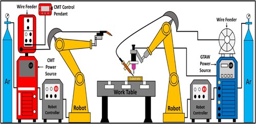
Table 1. Chemical composition (wt.-%) of In625 consumable wire and 90WNiFe substrate.
Three thin walls were fabricated with different heat input conditions (controlled by the arc current) used for the deposition of first two layers of In625 and the heat input was identical for subsequent layers. Here onwards, for convenience three thin walls are named as: low heat input (LHI), medium heat input (MHI), and high heat input (HHI). A current of 180 A, 200 A, and 220 A was employed for LHI, MHI, and HHI conditions, respectively. A total of 12 layers of In625 were deposited on the W-alloy substrate. The first two layers of In625 were deposited using the GTAW-based WAAM process with constant process parameters: TS (200 mm/min), WFR (2000mm/min), electrode-to-workpiece distance (5 mm), electrode tip angle (45°), torch angle (90°), and the shielding gas flow rate (15 L/min). From the third layer onwards, the CMT-WAAM process was utilised with constant process parameters: TS (300 mm/min), WFR (4000 mm/min), contact tip-to-workpiece distance (15 mm), torch angle (90°), and the shielding gas flow rate (15 L/min). Energy density and heat input were calculated using Equations (1 and 2) [Citation46]. [(a)–(c)] shows the images of the three thin walls of 90WNiFe/In625 BS. outlines layer-wise process parameters adopted for the fabrication of these thin walls. The rationale for using the GTAW-WAAM system to deposit the first two layers of In625 was to achieve strong bonding between 90WNiFe and In625, leveraging the high heat input and energy density of the GTAW process. However, starting from the third layer, the CMT-WAAM system was employed due to its comparatively lower heat input capability [Citation47], which helps in reducing residual stresses induced in the 90WNiFe substrate by the repetitive thermal cycles during the WAAM process [Citation48]. Although various heat inputs were adapted during the deposition of the first two layers using the GTAW-based WAAM, from the third layer onwards, identical heat input conditions were applied for all thin walls using the CMT-based WAAM. The deposition strategy employed for the preparation of BS is illustrated in (d). The dimensions (length × height × thickness) of thin walls deposited for LHI, MHI, and HHI conditions were 100 mm × 43.58 mm × 7.54 mm, 100 mm × 43.43 mm × 7.67 mm, and 100 mm × 43.38 mm × 8.68 mm, respectively.
Figure 2. (a)–(c) Thin walls of 90WNiFe/In625 BS fabricated with various heat inputs, (d) deposition strategy, and (e) tensile specimen dimensions.
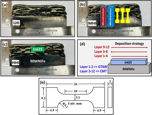
Table 2. Layer-wise process parameters for different heat input conditions.
Following the deposition process, the BS was sectioned along the build direction at specified locations, as illustrated in (b), to prepare samples for microstructure and microhardness testing, using the metallurgical saw. These samples were subsequently mounted and polished following the standard sample preparation procedures for metallography. Then the surfaces of the samples were grounded using SiC abrasives (grit sizes of 240–1200) and polished using diamond paste solutions of 3 μm and 1 μm size. To reveal the microstructure, the 90WNiFe side of polished samples was etched by Kroll’s reagent (a mixture of 92 mL of DI water, 6 mL of HNO3, and 2 mL of HF), and the In625 side was etched with aqua Regia etchant.
2.2. Microstructure characterisation
Microstructural analysis was conducted using an optical microscope (OM) and scanning electron microscope (SEM). For optical microscopy, a Nikon SMZ 1500 microscope was used for low-magnification images (up to 10× magnification), and a Nikon Eclipse MA1000 inverted microscope was used for higher-magnification images (up to 500× magnification). FEI Quanta 200 SEM equipped with an energy dispersive X-ray (EDX) and Hitachi SU7000 field emission SEM coupled with EDX was employed for microstructure and compositional analysis of 90WNiFe/In625 interface, 90WNiFe side and In625 side. For energy dispersive spectroscopy (EDS) analysis, the EDAX Octane Elect Super EDS system with EDAX APEX software was used. X-ray diffraction (XRD) was carried out to determine the phases present at the interface using the Rigaku Ultima IV XRD machine. For XRD analysis, the X-ray slit of 5 mm width was used to focus X-rays at the interface of polished and ground samples. Diffraction patterns were recorded using D/teX Ultra-High-Speed Detector. The raw data was imported into the PDXL software package for phase analysis and comparison with the standard patterns in the ICDD database.
2.3. Mechanical property testing
Microhardness tests were performed along the build direction of thin walls using a Buehler Wilson VH1202 microhardness tester with 500 g applied load (Vickers diamond indenter) and dwell time of 10 s. The Microhardness tester was equipped with an integrated high-resolution camera and DiametTM software. Three tensile specimens, following ASTM E8 standards, were prepared from each thin wall using wire electrical discharge machining (EDM), with dimensions illustrated in (e). Mechanical strength was investigated using the computer-controlled, uniaxial tensile testing system (TestResources 810 E4 Electrodynamic Test Machine). Tensile tests were conducted with an elongation rate of 0.001 s−. The failure characteristics and failure modes of fractured tensile specimens were examined using the FEI Quanta 200 SEM.
3. Results
3.1. Microstructure characterisation
shows the microstructural characteristics of the 90WNiFe/ In625 BS fabricated under three different heat input conditions: LHI, MHI, and HHI. Cross-sectional micrographs for each condition are displayed in (a, e, i), showcasing the bimetallic interface as well as the In625 and 90WNiFe regions, distinguished by their unique microstructures. Notably, there are no welding defects, such as voids, porosity, or cracks, at the interface of the three BS deposits as depicted in (c, g, k), indicating a robust metallurgical bond. It is evident from (c, g, k) that the size of the W grains near the interface is smaller for the LHI condition compared to the MHI and HHI conditions. This can be attributed to the increase in the heat-affected zone (HAZ) area with increasing welding heat input, which can be crucial in determining the W grain size close to the interface. Besides, the evapouration of Ni and Fe with increased heat input can also affect the W grain size at the interface, a concept to be explained in Section 4.2.
Figure 3. Optical microscopy images of 90WNiFe/In625 BS for LHI, MHI, and HHI conditions: Micrograph of the thin walls (a, e, i); In625 side (b, f, j); Interface (c, g, k); and 90WNiFe side (d, h, l).
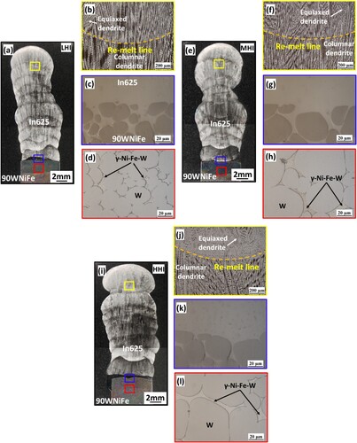
(d, h, l) displays the microstructure of the 90WNiFe substrate for LHI, MHI, and HHI conditions, respectively. The microstructure of the 90WNiFe alloy consists of a W matrix and γ-binding phase made of Ni, Fe, and W. Under higher magnification, the microstructure displays nearly spherical grains of W embedded within a solidified matrix phase containing a solid solution of Ni, Fe, and W. These microstructural features closely resemble those observed in 90WNiFe alloys produced using a variety of techniques, including spark plasma sintering [Citation7,Citation49], selective laser melting, and laser melting deposition [Citation33–37].
The deposited In625 shows a noticeable layer band structure along the direction of deposition height, as illustrated in (a, e, i). These layers are well-defined and easily distinguishable. The formation of layer bands can be attributed to the partial remelting and reheating cycles experienced by previously deposited layers during successive depositions [Citation32,Citation50]. (b, f, j) demonstrates the magnified images of the layer interface of deposited In625 for LHI, MHI, and HHI conditions, respectively, showcasing primarily columnar dendrites in the microstructure. These dendrites encompass several deposited layers, almost parallel to the build direction, and their formation is mainly determined by the direction of heat flow during the process. The heat mainly conducts from the molten pool to the underlying deposition layers on the substrate, and a limited amount of heat radiates to the air. Alongside columnar dendrites, equiaxed dendrites were also observed, as evident in (b, f, j), a microstructure morphology commonly observed by other researchers [Citation29,Citation31,Citation32] in WAAMed In625. The equiaxed dendrites are observed in the top layer of deposited In625. According to solidification theory, low values of temperature gradient(G) / Growth Rate(R) ratio results in equiaxed dendrites [Citation51]. In WAAM, the top layer does not undergo thermal cycles and re-melting, can be considered as the rapid solidification microstructure of In625 due to the faster cooling rate in the top layer. Low thermal gradients and high cooling rates in the top layer results in the formation of equiaxed dendrites.
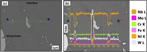
depict SEM images, EDS line scan, point scan, and area mapping results of the bimetallic interface for the LHI, MHI, and HHI conditions, respectively. In the case of LHI, elemental mapping is conducted on the area specified in (b). The findings reveal notable diffusion of chromium (Cr), Nickel (Ni), Molybdenum (Mo), and Niobium (Nb) from the In625 side into the γ-(Ni, Fe, and W) binding matrix of 90WNiFe. Particularly, Cr and Ni exhibit higher diffusion compared to other elements like Mo and Nb, owing to their higher solubility in the Ni/Fe matrix [Citation52]. In addition, small traces of W and Fe are detected in the In625 region. Point scans at points P1 and P2 further confirm the presence of W and Fe, as depicted in (e). This indicates increased mixing of alloying elements from both 90WNiFe and In625 during deposition, facilitating the formation of multi-component phases near the interface. From EDS area mapping results, it is also noted that the alloying elements (Cr, Fe, Mo, Nb) were not diffused into W matrix of 90WNiFe substrate due to the comparatively high melting point of W [Citation34]. The magnified SEM images in (a) reveal precipitates with distinct light and dark contrast. Elemental composition analysis of these phases (points P3 and P4) illustrated in (e) indicates that the composition is mostly comprised of Ni, Cr, W, Mo, and Nb. Similar phases are detected in MHI and HHI conditions, with corresponding compositions shown in and (e). To further confirm the presence of these elements, elemental line scan was performed across these phases from line AB, as indicated by the green line in (a). (b) illustrates the compositional variation across the same line, indicating the presence of two distinct regions (phases). The white area predominantly consists of W, Ni with a less amount of Cr, while the gray area is Ni and Cr-rich with a lesser amount of W. These precipitates are primarily formed due to elemental segregation at the deposition temperature. The higher amount of Cr at the interface leads to the creation of Cr-rich and Cr-depleted regions due to segregation, resulting in the formation of these precipitates. The formation of Cr and W-rich precipitates around 1300°C was also observed by Dilberto et al. [Citation53] during an oxidation experiment of Mo-W-based alloys.
Figure 4. For the LHI, the SEM images depicting: (a) In625 side adjacent to the interface, (b) 90WNiFe/In625 interface and corresponding EDS elemental area mapping, and (c) 90WNiFe side adjacent to the interface; (d) EDS line scan performed at the interface indicated in Figure (b) by the black dashed line, and (e) EDS point scan results at the locations shown in Figure (a, b, c).
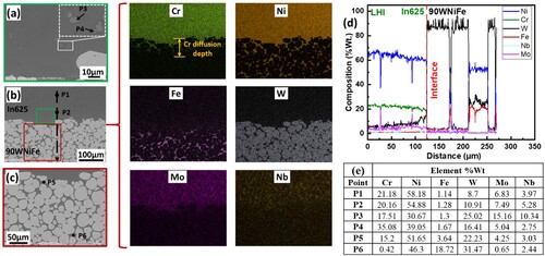
Figure 5. For the MHI, the SEM images depicting: (a) In625 side adjacent to the interface, (b) 90WNiFe/In625 interface and corresponding EDS elemental area mapping, and (c) 90WNiFe side adjacent to the interface; (d) EDS line scan performed at the interface indicated in Figure (b) by the black dashed line, and (e) EDS point scan results at the locations shown in Figure (a, b, c).
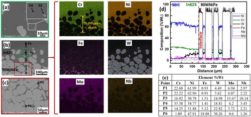
Figure 6. For the HHI, the SEM images depicting: (a) In625 side adjacent to the interface, (b) 90WNiFe/In625 interface and corresponding EDS elemental area mapping, and (c) 90WNiFe side adjacent to the interface; (d) EDS line scan performed at the interface indicated in Figure (b) by the black dashed line, and (e) EDS point scan results at the locations shown in Figure (a, b, c).
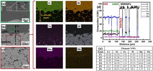
Figure 7. (a) Magnified SEM image for inset of (a) along with EDS scan location indicated by line AB and (b) line scan data showing compositional variation along line AB.
As compared to the LHI condition, the diffusion depth of the alloying elements is higher in the MHI and HHI conditions, as evident from the EDS area mapping results shown in . It is evident from the elemental area mapping images of Cr that as the heat input increases the diffusion depth of Cr increases. This can be attributed to the effect of temperature variation at different heat input conditions. With increased heat input, the arc temperature rises, increasing the temperature of the melted γ-(Ni, Fe, W) binding phase. This increase in temperature elevates the activation energy of the alloying elements, promoting their diffusion into the γ-(Ni, Fe, W) matrix of 90WNiFe [Citation54]. Line scan results presented in (d) also support the increase in diffusion depth with heat input conditions. Points P5 and P6 shown in (c) are located in two different regions close to the interface for all heat input conditions. Elemental analysis from P5 indicates the presence of a high amount of Ni, Cr, and W, suggesting a possible Cr-Ni-W solid solution formed during solidification at the deposition temperature. On the other hand, P6 primarily contains Ni, Fe, and W, indicating the prevalent γ-binding phase of the 90WNiFe substrate. Notably, the increased presence of W in the γ-binding phase indicates partial dissolution of W into the Ni-Fe matrix. This phenomenon can be attributed to the different solubilities of W, Ni, and Fe in W-Ni-Fe systems. W exhibits high solubility in the Ni/Fe matrix, while the solubility of Ni and Fe in tungsten is practically negligible [Citation55–57]. Typically, with an increase in temperature, the dissolution rate of W should also increase, leading to a higher W content at the point P5 point compared to the P6 point. However, the EDS point scan data shows that the binding phase actually has a lower W content at P5 than at P6. Simultaneously, the P5 point contains higher amounts of Cr and Ni than the P6 point. This discrepancy can be attributed to the higher diffusion rates of Ni and Cr at the deposition temperature, especially near the interface [Citation52,Citation58]. Furthermore, as shown in , fine precipitates rich in W are formed closer to the interface, indicating increased dissolution of W at these specific locations. These precipitates, which form through a dissolution-precipitation phenomenon, were not observed at the P6 point. This suggests a localised variation in the dissolution and precipitation process, influenced by the temperature gradient and the compositional changes near the interface. Depending on the heat input condition, the depth of the Cr-Ni-W solution near the interface will increase due to the increased diffusion of Cr and Ni into the γ-(Ni, Fe, W) matrix of 90WNiFe substrate, which was also visible from the EDS area mapping. The formation of this Cr-Ni-W FCC phase plays a crucial role in the bonding of these two alloys. The bonding mechanism for 90WNiFe and In625 will be discussed in detail in section 4.1. The dilution level/ratio for W at the interface was calculated using an equation developed by DuPONT et al. [Citation59] by considering the elemental composition at the interface. The calculated dilution levels of W were 0.17, 0.20, and 0.22 for LHI, MHI, and HHI conditions, respectively. The dilution level increases with the increase in heat input condition, which is consistent with the findings of Pandey et al. [Citation60].
To predict the presence of various phases at the bimetallic interface, an equilibrium cooling calculation was carried out using the CALculation of PHAse Diagrams (CALPHAD) approach with a 50:50 mixture of two alloys. The temperature range was selected between 400-2000°C encompassing the whole temperature spectrum experienced during deposition. The corresponding results are indicated in (a). From the calculation, the major phases identified are BCC-W, BCC-Cr, and FCC-Ni. Besides, the presence of a ternary P-phase (Ni24Cr20Mo12) was also indicated. Furthermore, the characteristic γ-Ni3Nb phase of Inconel alloy was also predicted in the equilibrium calculation. The solidification of Ni is predicted to start around 1320°C with a decreasing liquid phase fraction. With the continuation of solidification, the γ-Ni3Nb phase starts forming at around 800°C with a corresponding decrease in the Ni FCC-Ni phase fraction. This phase was also identified in the XRD experiments conducted at the interface for 2θ = 30°–100° with a step size of 0.02.
Figure 8. (a) Equilibrium-cooling phase calculation of 50:50 mixture (by weight) of 90WNiFe and In625; XRD Results for (b) Interface (LHI, MHI, and HHI conditions), (c) 90WNiFe side, and (d) In625 side.
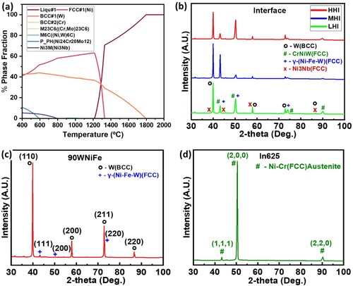
The XRD results are displayed in (b) for all heat input conditions. The major phases identified include BCC-W, FCC-Cr-Ni-W, and FCC-γ-(Ni-Fe-W). The major peaks of the BCC-W phase were found at 2θ = 39.92°, 57.89°, 72.84°, and 86.66°, corresponding to the BCC crystal planes of (110), (200), (211), and (220), respectively. For γ-(Ni-Fe-W), phase peaks were observed at 2θ = 43.18°, 50.16°, and 73.04°, corresponding to the FCC crystal planes of (111), (200), and (220), respectively. The Cr-Ni-W solid solution phase was also identified at 2θ = 43.16°, 50.06°, 73.99°, and 90.09° corresponding to the FCC crystal planes of (111), (200), (220), and (311), respectively. The presence of such a phase was also identified at the interface from the EDS point analysis discussed earlier. From (b), it is evident that the location of the peaks matches closely in each of the heat input conditions, suggesting that there is no substantial peak shift under varied heat input conditions. It is seen that the interface includes all the major peaks of In625 and 90WNiFe alloys, as displayed in (c) and (d). Similar peaks were reported by Wang et al. [Citation25], Ravi et al. [Citation31], Jiang et al. [Citation32], and Tanvir et al. [Citation27], for WAAMed In625. The detection results also agreed well with the XRD results of the 90WNiFe alloy prepared by spark plasma sintering [Citation7,Citation49], selective laser melting, and laser melting deposition [Citation33–37].
When comparing the XRD results with the CALPHAD prediction, it is seen that there is a good correlation between the calculated and detected phases for all the major phases. However, some discrepancies exist for the minor phases, including the presence of the P-phase, which was originally predicted in the calculation. Besides, the presence of a solid solution with Cr-Ni-W was not present in the phase calculation, although it had a significant presence in the microstructure close to the interface. This happens mostly because of the non-equilibrium thermal cycles experienced during the wire-based DED process [Citation50]. Due to complex thermal characteristics, elemental segregation exists during solidification, which can impose compositional variation across the interface. Evidence of this segregation is also evident in the EDS point scan taken closer to the interface shown in .
3.2. Mechanical properties
3.2.1. Microhardness
Microhardness tests were performed along the build direction on the three thin walls, and the profiles of the entire deposit, including the bimetallic interface, are presented in (a–c). Hardness was measured from the bottom of the 90WNiFe substrate to the top of the In625 deposit. The entire microhardness profile can be divided into three regions: the 90WNiFe side, the heat-affected zone (HAZ), and the In625 side. The hardness values on the 90WNiFe substrate and the In625 sides differ significantly, as shown in (a, b, c). The average hardness of the 90WNiFe substrate for LHI was 338.0 ± 8.4 HV, with a minimum of 326.1 HV and a maximum of 355.1 HV. In the MHI, the average hardness of the 90WNiFe substrate was 348.8 ± 13.0 HV, ranging from 329.0 HV to 372.4 HV. For HHI, the hardness of the 90WNiFe substrate ranges from 324.0 HV to 364.9 HV, with an average value of 340.2 ± 10.6 HV. Overall, for all three conditions, the average hardness of the 90WNiFe substrate was in the range of 338.0–348.8 HV, which is typical of liquid-phase sintered components of this specific alloy [Citation6].
Figure 9. Microhardness profiles for (a) LHI thin-wall, (b) MHI thin-wall, (c) HHI thin-wall, and (d) comparison of the microhardness at various locations of 90WNiFe/In625 thin-wall.
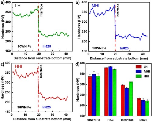
In the HAZ of 90WNiFe, a maximum hardness of 380.2 ± 2.7 HV, 385.6 ± 2.3 HV, and 372.4 ± 2.4 HV was observed for the LHI, MHI, and HHI conditions, respectively. A slight increase in hardness was observed in the HAZ section of 90WNiFe adjacent to the interface. Various metallurgical phenomena, such as diffusion of elements, work hardening, dislocation density, grain refinement, and precipitation at the interface, may have caused an increase in hardness, as suggested by Kou [Citation51]. In this study, the migration of Cr into the γ-(Ni, Fe, W) matrix of the substrate as well as the W grain growth could primarily be responsible for the increase in hardness in the HAZ section. The migrated Cr causes a solid-solution strengthening effect, thereby increasing the hardness. The hardness at the bimetallic interface was measured to be 298.6 ± 3.2 HV, 282.7 ± 4.4 HV, and 313 ± 3.5 HV, respectively. There is a decrease in the hardness value at the bimetallic interface as compared to the hardness of the HAZ section and substrate, which suggests that no hard precipitates or phases are formed at the interface, which is also evident from the XRD results of the interface presented in (b). The average hardness of the In625 region is 234.0 ± 6.4 HV, with a minimum of 223.1 HV and a maximum of 246.1 HV for LHI conditions. In the MHI, the average hardness of the In625 side is 225.5 ± 7.1 HV, and the values range from 207.4 HV to 240.7 HV. For HHI, the hardness of deposited In625 ranges from 208.4 HV to 247.5 HV, with an average value of 222.2 ± 8.5 HV. Overall, for all three conditions, the average hardness of the In625 side was in the range of 222.2 to 234.0 HV. The result is comparable to the welded [Citation61] and as-deposited WAAMed In625 or similar alloys [Citation27,Citation29,Citation31,Citation32]. The comparison results of hardness at different locations of the deposit for three heat input conditions are summarised in (d). The HAZ of 90WNiFe has the highest hardness as compared to other regions, however bimetallic interface has a hardness lower than the HAZ and 90WNiFe substrate. In625 deposit exhibited the lowest hardness.
3.2.2. Tensile test and fractography
Tensile samples were prepared from each thin wall along the build direction and tested at room temperature. The tensile test results for the 90WNiFe/In625 BS are shown in . The stress–strain curves illustrate that all the samples underwent considerable deformation before fracture. The results of the tests are summarised in . In the LHI, the average ultimate tensile strength was 618 ± 12.38 MPa, with the LHI samples exhibiting the highest average deformation of 49 ± 1.69%. The average UTS of the MHI condition was 601 ± 23.63 MPa, with an average elongation of 31 ± 6.36%. In the HHI condition, the average UTS was 594 ± 15.24 MPa and the elongation was 26 ± 4.27%. It is noted that due to an instrument malfunctioning, the test data for one sample of HHI was not acquired. Among the three conditions, the LHI samples demonstrated the greatest average UTS and elongation. However, the HHI condition exhibited the lowest average elongation and UTS. (d) depicts a comparison of average yield strength (YS), UTS, and elongation among three different heat-input conditions. It was also observed that elongation decreases with increasing heat input, while YS shows insignificant variation. Overall, UTS and elongation of the fabricated BS varied between 578–634 MPa and 21–51%, respectively. From existing literature, WAAMed In625 has YS, UTS, and elongation of 373, 658 MPa, and 56%, respectively [Citation28], whereas 90WNiFe manufactured by liquid phase sintering has UTS of approximately 758 MPa, YS of 517 MPa, and elongation of 5% [Citation6]. As a result, the BS has a UTS below that of 90WNiFe and is comparable to In625 alloy. However, it is interesting that the ductility of 90WNiFe/In625 BS is greater than that of the parent alloy 90WNiFe. Furthermore, the YS of the bimetallic structure is almost similar to that of the WAAMed In625.
Figure 10. Stress-strain curve: (a) LHI, (b) MHI, and (c) HHI; (d) Comparison of Avg. YS, UTS, and elongation.
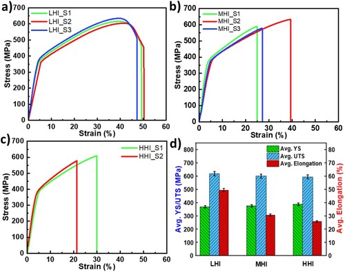
Table 3. Summary of the tensile test results for different conditions.
The tensile fracture surfaces were characterised and analyzed using SEM. For convenience, the fracture surface of the specimen with the highest elongation in each heat input condition has been displayed. shows the fractured tensile specimens along with SEM images of the fractured surfaces at different magnifications. Overall, for all three heat-input conditions, the tensile specimens failed at different locations and exhibited different fracture modes. The LHI condition samples failed on the In625 matrix in a ductile manner, with maximum elongation. During tensile testing, the In625 part of the gauge section elongated more than 90WNiFe, as In625 was more ductile than 90WNiFe [Citation6,Citation28]. The In625 side of the tensile specimens underwent considerable necking, as illustrated in (a), and failed on the In625 side. The overall fractured surface seems to consist of shear lip and fibrous regions only, owing to the inherently ductile nature of In625. A large number of elongated dimples of different sizes, along with voids, are present on the fracture surface, which resembles a typical ductile fracture, as indicated in (a1-a3). The EDS point scan results of the fractured surface of the LHI tensile specimens, summarised in , revealed a composition corresponding to the In625 alloy.
Figure 11. (a)–(c) Fractured samples; SEM images of fractured tensile samples: LHI (a1–a3), MHI (b1–b3), and HHI (c1–c3).
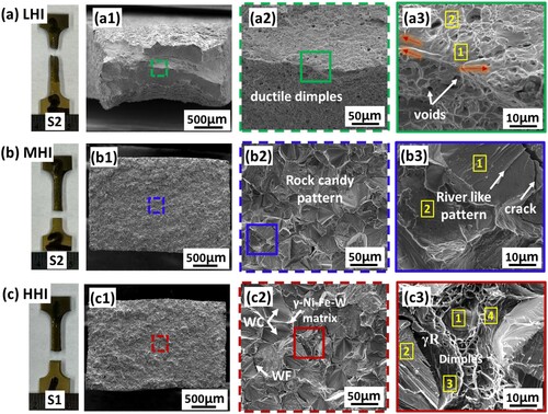
Table 4. EDS point scan results of fracture surfaces of tensile samples for different heat input conditions.
From (b), it was observed that the MHI condition samples failed exactly at the interface in a brittle manner, although the samples underwent elongation of 25-39%. The magnified SEM images of the fractured surface of the MHI condition sample refer to (b2-b3) demonstrated mixed trans granular and intergranular fractures with river-like and rock-candy morphologies. Trans granular and intergranular cracks in the W grains can be observed in the SEM images. EDS point scan analysis of the fracture samples was performed. The locations of the points denoted in (b3) and the corresponding elemental compositions are listed in . The elemental composition of point 1 showed W with wt. % of above 95%, indicating a purely W matrix. The W matrix exhibited a river-like fracture morphology. However, point 2 is located in the γ-(Ni, Fe, W) matrix, showing all elements (Cr, Ni, Fe, W, Mo, and Nb) in the EDS point scan results, suggesting failure occurred at the interface.
As illustrated in (c), tensile specimen of the HHI condition failed near the interface on the 90WNiFe matrix side. SEM images of fractured specimen are illustrated in (c1-c3). In general, 90WNiFe has four fracture modes: intergranular fracture of W grains (WF), intra(trans)granular fracture of W grains (WC), interfacial debonding of W grains-binding phase (W/γD), and ductile tearing of binding phase (γR) [Citation5]. From (c1-c3), the fracture morphology of specimen reveals intergranular (WF) and trans-granular fracture (WC) of W grains along with ductile tearing of the binder phase (γR). The W matrix shows river/cleavage morphology; however, the Ni-Fe-W matrix phase shows ductile dimples. Ni-Fe-W matrix shows ductile tearing along with voids, as illustrated in (c3). A similar type of fracture morphology was observed for 90WNiFe prepared by spark plasma sintering [Citation7,Citation49], selective laser melting, and laser melting deposition [Citation33–37]. EDS point scan results of the fractured surface of the HHI tensile specimen are summarised in . Points 1 and 2 are located at the W matrix showing elements W, Ni, and Fe with wt. % of W above 95%. The elemental composition of points 3 and 4 (located in the binding matrix) shows all elements (Cr, Ni, Fe, W, Mo, Nb) in EDS point scan results representing sample failed near interface on 90WNiFe side.
4. Discussion
4.1. Bonding mechanism
Dissimilar material interfacial bonding is usually achieved through element diffusion, and element mixing in the melt pool including the capillary effect. In fusion welding, bonds between dissimilar metals are established by the formation and solidification of a liquid phase at the interface. In some cases, an interlayer of different material having metallurgical compatibility with both parent metals is introduced between the parent metals to facilitate diffusion bonding [Citation62]. The interlayer reduces the melting point of one or both of the parent alloys to form a liquid phase and improves diffusion capability, resulting in the formation of strong metallurgical bonds. However, in the present study, the In625 was deposited on a 90WNiFe substrate without any interlayer. Besides, In625 has a melting point significantly below that of the pure W, suggesting that melting of the W-phase in 90WNiFe is not expected. Therefore, the bonding mechanism of the WAAM 90WNiFe/In625 bimetallic structure is different compared to interlayer bonding.
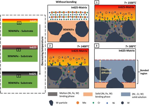
displays the interfacial bonding mechanism of 90WNiFe /In625, which involves three distinct steps: (1) liquid phase formation, (2) elemental diffusion, and (3) the formation of solid solutions. The substrate contains a low melting point γ-(Ni, Fe, W) binding phase [Citation34]. During the deposition of the 1st layer of the In625, a portion of this binding phase close to the interface undergoes melting. This creates micro-pools at the substrate close to the interface, which promotes the diffusion of elements from In625 to γ-(Ni-Fe-W) matrix. The diffusion of Cr, Ni, Mo, and Nb from molten In625 into the γ-(Ni-Fe-W) binding phase is evident from the EDS elemental mapping as displayed in for all heat input conditions. Compared to the liquid binding phase, diffusion of Cr into the W-phase is less, which can be attributed to the different solubilities of Cr in the γ-(Ni, Fe, W) binding phase and W matrix. Cr has a high solubility in the Ni/Fe matrix [Citation52], but the solubility of Cr in W is less due to a miscibility gap below 1677°C [Citation63]. At the same time, Ni atoms also diffuse into the 90WNiFe side from the deposited In625 side, causing a continuous distribution of Ni throughout the interface. Nevertheless, from the elemental mapping, it is evident that the presence of Fe at the interface is not significant. Considerable diffusion of Mo and Nb atoms is also visible from the EDS mapping results depicted in . During solidification, at the interface, Cr, Ni, and W form a solid solution containing a high amount of Ni. The elemental composition data of the point scan at P5 point as shown in confirms the presence of a Cr-Ni-W phase. From XRD results, such a solid solution phase (Cr-Ni-W phase) is also evident at 2θ = 43.16°, 50.06°, 73.99°, and 90.09°. The presence of a Ni-rich γ-solid solution is also indicated in the Ni-Cr-W ternary system [Citation64]. This implies that some W atoms are also diffusing into the micro-pool, which is formed during the deposition process. As the heat transfer is comparatively fast owing to the higher thermal conductivity of the 90WNiFe substrate, the diffusion boundary is restricted up to around 50–100 microns. This boundary is indicated in by the red dotted line, which also represents the bonded region for this BS. Thus, diffusion of Cr, Ni, Mo, and Nb from molten In625 into the γ-(Ni-Fe-W) binding phase and formation of Ni-Cr-W solid solution is responsible for good metallurgical bonding of 90WNiFe/In625 BS.
Figure 12. Bonding mechanism of 90WNiFe/In625 during wire-arc DED process.
4.2. Correlation between process parameters and interfacial microstructure
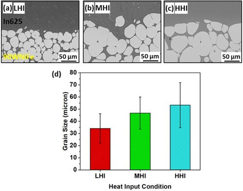
shows SEM images of the BS interface under LHI, MHI, and HHI conditions. Visually inspection reveals that the size of W grains at the interface is greater for MHI and HHI conditions compared to the LHI condition. To quantify the grain size, ImageJ software was utilised. (d) shows a quantitative comparison of grain sizes for different heat input conditions. For the LHI case, the average W grain size was measured at 34.11 µm, with a standard deviation of 12.08 µm. In contrast, for MHI and HHI conditions, these values were 46.67 ± 13.22 µm and 53.28 ± 18.55 µm, respectively. As the heat input increases, W grain size also increases, this is attributed to the evapouration of Ni and Fe during the deposition of the 1st layer of In625 on the 90WNiFe substrate [Citation35]. The melting point of W (3422 °C) is significantly higher than that of the Ni-based binder matrix (1455 °C for pure Ni) and is even higher than the boiling point of the Ni-based binder matrix (2730 °C for pure Ni) [Citation34]. Due to the very high vapour pressure of binder elements (Ni, Fe), with increasing temperature, preferential evapouration of binder elements can be predicted during the deposition process. In the LHI condition, heat input (810 J/mm) is the lowest among the three conditions causing lower arc temperature during the deposition of 1st layer of In625 on 90WNiFe substrate. Accordingly, the formation of a liquid phase between the W grains adjacent to the bimetallic interface was minimal, making it difficult for the W grains to rearrange and grow in size. Additionally, in the LHI condition, the evapouration of Ni and Fe is less as compared to the MHI and HHI conditions. As a result, under the LHI condition, the size of W grains adjacent to the bimetallic interface is smaller compared to the other two conditions. In contrast, for the MHI (Heat Input: 900 J/mm) and HHI (Heat Input: 990 J/mm) conditions, arc temperature is substantially higher. This elevated temperature increases the molten pool temperature, resulting in the evapouration of Ni and Fe elements from the binding phase, facilitating favourable conditions for W grain growth. The W grains continued to grow due to the constant dissolution and precipitation of the solid phase [Citation7]. Due to the evapouration of Ni and Fe elements, the liquid binding phase diminishes, reducing the effectiveness of the densification process and allowing W grains to grow more freely. Also, the evapouration of Ni and Fe decreases the segregation of these elements at the grain boundaries of W, leading to less resistance against grain boundary movement. As a result, the small W grains can rearrange, bond together, and grow in size. Consequently, in MHI and HHI conditions, the size of W grains adjacent to the bimetallic interface is greater as compared to the LHI condition. This phenomenon is consistent with observations in other processes such as liquid phase sintering [Citation65], spark plasma sintering of tungsten alloys at different temperatures [Citation7], and laser melting deposition of 90WNiFe alloy at different laser power [Citation35].
Figure 13. SEM Images of BS interface: (a) LHI, (b) MHI, (c) HHI, and (d) comparison of W grain size.
4.3. Correlation between microstructure and mechanical properties
The elemental diffusion across the 90WNiFe/In625 interface and the resulting microstructures determine the mechanical properties of the fabricated structures. The microhardness profiles revealed a distinct variation in hardness across the 90WNiFe substrate, the HAZ of 90WNiFe, the 90WNiFe/In625 interface, and the In625 deposit. The HAZ of 90WNiFe substrate exhibited a significant increase in hardness, likely due to Cr diffusion from In625 into γ-(Ni, Fe, W) matrix, forming a Cr-Ni-W solid solution and subsequent solid-solution strengthening. Additionally, the presence of hard Ni3Nb phase further enhanced hardness in the HAZ of 90WNiFe. The hardness reached its maximum value at the HAZ of 90WNiFe adjacent to the 90WNiFe/In625 interface.
Tensile samples of LHI condition demonstrated the greatest average UTS and elongation, which can be attributed to smaller W grain size at the interface as depicted in . Smaller W grains are surrounded by γ-(Ni, Fe, W) binding matrix. During tensile testing the γ-(Ni, Fe, W) binding matrix also deforms along with In625 and imparts ductility to BS. As a result, comparatively, smaller grain size of W in LHI contributed to the slightly higher interfacial bond strength, thereby altering the fracture location to the In625 deposit. As a result, LHI samples failed in ductile manner as illustrated in (a1–a3). However, in MHI and HHI, the higher W grain size increased the total volume of W grains at the interface. These large W grains are prone to forming microcracks during tensile test. Additionally, higher heat inputs in MHI and HHI reduced amount of γ-(Ni, Fe, W) binding phase due to evapouration of Ni and Fe elements. Higher W grain size and less amount of binding phase, resulted in lowering UTS and elongation of MHI and HHI tensile sample. Consequently, the HAZ of 90WNiFe adjacent to the 90WNiFe/In625 interface served as a critical location of fracture for the samples prepared with MHI and HHI. The elevated hardness in this region could lead to the inhiation of microcracks during tensile testing, which lead to brittle fracture with microcracks primarily formed in the W grains as illustrated in (b1–b3) and 11(c1–c3).
5. Conclusion
This study aimed to fabricate 90WNiFe/In625 bimetallic structures via wire-arc DED based AM. Bimetallic structures were successfully fabricated under multiple heat input conditions, with no visible defects such as cracks or porosity observed at the interface.
The interface exhibited an absence of welding defects such as cracks and porosity, presenting an intimate and robust metallurgical bond between the 90WNiFe and In625. The microstructure of the 90WNiFe side comprises spherical tungsten grains and a γ-(Ni-Fe) matrix phase with dissolved tungsten, whereas the In625 deposit consists of elongated columnar and equiaxed dendrites.
The 90WNiFe/In625 interface demonstrated the diffusion of Cr, Ni, Mo, and Nb from the In625 into the γ-(Ni, Fe, W) binding matrix of the 90WNiFe. The formation of Ni-Cr-W solid solution was responsible for imparting the bonding strength to BS.
A slight increase in hardness at the heat-affected zone of 90WNiFe was observed, resulting from chromium diffusion into the γ-(Ni, Fe, W) matrix and W grain growth near the interface. However, a decrease in hardness value at the interface suggests that no hard compounds or phases are formed at the interface.
The 90WNiFe/In625 bimetallic structure fabricated under comparatively low heat input condition achieved highest ultimate tensile strength of 618 ± 12.38 MPa and the greatest elongation of 49 ± 1.69%. The elongation of BS was greater than that of thes parent alloy 90WNiFe. Within the investigated range of heat input, the ultimate strength did not significantly change as the heat input increased, however, there was a substantial decrease in elongation as heat input increased.
Tensile samples from all three heat input conditions failed at distinct locations and exhibited varying fracture modes. The low heat input condition samples failed within the In625 matrix in a ductile manner, with a large number of dimples on fractured surfaces. Conversely, samples from medium heat input failed at the bimetallic interface and high heat input conditions samples failed near the bimetallic interface on the 90WNiFe side in a brittle manner.
This research provides a comprehensive investigation of the microstructures and mechanical properties of WAAM-fabricated 90WNiFe/In625 bimetallic structures which laid the foundation for the future research direction. The Authors plan to expand this work by further investigating mechanical properties at high temperatures, thermal properties, and the application of stress relief heat treatments to enhance the performance of this bimetallic structure to leverage its inherent advantages. Additionally, the authors will investigate residual stresses using experimental and computational methods.
Disclosure statement
No potential conflict of interest was reported by the author(s).
Data availability statement
Authors agree to make data and materials supporting the results or analyses presented in their paper available upon reasonable request.
Additional information
Funding
References
- Bandyopadhyay A, Zhang Y, Onuike B. Additive manufacturing of bimetallic structures. Visual Phys Prototyp. 2022;17:256–294. DOI:10.1080/17452759.2022.2040738
- Camacho AM, Rodríguez-Prieto A, Manuel Herrero J, et al. An experimental and numerical analysis of the compression of bimetallic cylinders. Materials. 2019;12:4094. DOI:10.3390/MA12244094
- Li D, Liu Q, Wang W, et al. Corrosion behavior of AISI 316L stainless steel used as inner lining of bimetallic pipe in a seawater environment. Materials. 2021;14:1539. DOI:10.3390/MA14061539
- Bose A, Schuh CA, Tobia JC, et al. Traditional and additive manufacturing of a new Tungsten heavy alloy alternative. Int J Refract Met Hard Mater. 2018;73:22–28. DOI:10.1016/J.IJRMHM.2018.01.019
- Liu W, Ma Y, Zhang J. Properties and microstructural evolution of W-Ni-Fe alloy via microwave sintering. Int J Refract Met Hard Mater. 2012;35:138–142. DOI:10.1016/J.IJRMHM.2012.05.004
- High Density Tungsten Alloy (WNiFe) Sheets, (n.d.) [cited 11 Sep 2023]. https://www.albmaterials.com/metals-and-alloys/743-high-density-tungsten-alloy-wnife-sheets.html.
- Xiang DP, Ding L, Li YY, et al. Microstructure and mechanical properties of fine-grained W–7Ni–3Fe heavy alloy by spark plasma sintering. Mater Sci Eng A. 2012;551:95–99. DOI:10.1016/J.MSEA.2012.04.099
- Dinda GP, Dasgupta AK, Mazumder J. Laser aided direct metal deposition of Inconel 625 superalloy: microstructural evolution and thermal stability. Mater Sci Eng A. 2009;509:98–104. DOI:10.1016/J.MSEA.2009.01.009
- Kim K-S, Kang T-H, Kassner ME, et al. High-temperature tensile and high cycle fatigue properties of inconel 625 alloy manufactured by laser powder bed fusion. Addit Manuf. 2020;35:101377. DOI:10.1016/j.addma.2020.101377
- Wang Z, Guan K, Gao M, et al. The microstructure and mechanical properties of deposited-IN718 by selective laser melting. J Alloys Compd. 2012;513:518–523. DOI:10.1016/J.JALLCOM.2011.10.107
- Huebner J, Kata D, Kusiński J, et al. Microstructure of laser cladded carbide reinforced Inconel 625 alloy for turbine blade application. Ceram Int. 2017;43:8677–8684. DOI:10.1016/J.CERAMINT.2017.03.194
- Ramkumar KD, Abraham WS, Viyash V, et al. Investigations on the microstructure, tensile strength and high temperature corrosion behaviour of Inconel 625 and Inconel 718 dissimilar joints. J Manuf Process. 2017;25:306–322. DOI:10.1016/J.JMAPRO.2016.12.018
- Hosseini E, Popovich VA. A review of mechanical properties of additively manufactured Inconel 718. Addit Manuf. 2019;30:100877. DOI:10.1016/J.ADDMA.2019.100877
- Ghanavati R, Naffakh-Moosavy H. Additive manufacturing of functionally graded metallic materials: a review of experimental and numerical studies. J Mater Res Technol. 2021;13:1628–1664. DOI:10.1016/j.jmrt.2021.05.022
- Bandyopadhyay A, Heer B. Additive manufacturing of multi-material structures. Mater Sci Eng R Rep. 2018;129:1–16. DOI:10.1016/J.MSER.2018.04.001
- Wang D, Liu L, Deng G, et al. Recent progress on additive manufacturing of multi-material structures with laser powder bed fusion. Virtual Phys Prototyp. 2022;17:329–365. DOI:10.1080/17452759.2022.2028343
- Jadhav S, Abdul Karim M, Bong Kim D. Bimetallic structure of TZM and NbZr1 fabricated by wire-based directed energy deposition. Mater Lett. 2024;356:135605. DOI:10.1016/J.MATLET.2023.135605
- Jadhav S, Bajestani MS, Islam S, et al. Materials characterization of Ti6Al4 V to NbZr1 bimetallic structure fabricated by wire arc additive manufacturing. Mater Today Commun. 2023;36:106934. DOI:10.1016/J.MTCOMM.2023.106934
- Frazier WE. Metal additive manufacturing: a review. J Mater Eng Perform. 2014;23:1917–1928. DOI:10.1007/s11665-014-0958-z
- Bevans B, Ramalho A, Smoqi Z, et al. Monitoring and flaw detection during wire-based directed energy deposition using in-situ acoustic sensing and wavelet graph signal analysis. Mater Des. 2023;225:111480. DOI:10.1016/j.matdes.2022.111480
- Felice IO, Shen J, Barragan AFC, et al. Wire and arc additive manufacturing of Fe-based shape memory alloys: microstructure, mechanical and functional behavior. Mater Des. 2023;231:112004. DOI:10.1016/j.matdes.2023.112004
- Kushwaha AK, Rahman MH, Slater E, et al. Powder bed fusion–based additive manufacturing: SLS, SLM, SHS, and DMLS. Tribol Addit Manuf Mater Fundam Model Appl. 2022;1–37. DOI:10.1016/B978-0-12-821328-5.00001-9
- Jin W, Zhang C, Jin S, et al. Wire arc additive manufacturing of stainless steels: a review. Appl Sci. 2020;10; DOI:10.3390/app10051563
- Zhang C, Yu H, Sun D, et al. Fabrication of multi-material components by wire arc additive manufacturing. Coatings. 2022;12:1683. DOI:10.3390/COATINGS12111683
- Wang JF, Sun QJ, Wang H, et al. Effect of location on microstructure and mechanical properties of additive layer manufactured Inconel 625 using gas tungsten arc welding. Mater Sci Eng A. 2016;676:395–405. DOI:10.1016/J.MSEA.2016.09.015
- Rodrigues TA, Cipriano Farias FW, Avila JA, et al. Effect of heat treatments on Inconel 625 fabricated by wire and arc additive manufacturing: an in situ synchrotron X-ray diffraction analysis. Sci Technol Weld Join. 2023;2023:534–539. DOI:10.1080/13621718.2023.2187927
- Tanvir ANM, Ahsan MRU, Ji C, et al. Heat treatment effects on Inconel 625 components fabricated by wire + arc additive manufacturing (WAAM)—part 1: microstructural characterization. Int J Adv Manuf Technol. 2019;103:3785–3798. DOI:10.1007/S00170-019-03828-6/METRICS
- Tanvir ANM, Ahsan MRU, Seo G, et al. Heat treatment effects on Inconel 625 components fabricated by wire + arc additively manufacturing (WAAM)—part 2: mechanical properties. Int J Adv Manuf Technol. 2020;110:1709–1721. DOI:10.1007/S00170-020-05980-W/METRICS
- Votruba V, Diviš I, Pilsová L, et al. Experimental investigation of CMT discontinuous wire arc additive manufacturing of Inconel 625. Int J Adv Manuf Technol. 2022;122:711–727. DOI:10.1007/s00170-022-09878-7
- Yangfan W, Xizhang C, Chuanchu S. Microstructure and mechanical properties of Inconel 625 fabricated by wire-arc additive manufacturing. Surf Coat Technol. 2019;374:116–123. DOI:10.1016/J.SURFCOAT.2019.05.079
- Ravi G, Murugan N, Arulmani R. Microstructure and mechanical properties of Inconel-625 slab component fabricated by wire arc additive manufacturing. Mater Sci Technol. 2020;36:1785–1795. DOI:10.1080/02670836.2020.1836737
- Jiang Q, Zhang P, Yu Z, et al. Microstructure and mechanical properties of thick-walled Inconel 625 alloy manufactured by wire arc additive manufacture with different torch paths. Adv Eng Mater. 2021;23:1–13. DOI:10.1002/adem.202000728
- Li J, Wei Z, Zhou B, et al. Densification, microstructure and properties of 90W-7Ni-3Fe fabricated by selective laser melting. Met. 2019;9:884. DOI:10.3390/MET9080884
- Iveković A, Montero-Sistiaga ML, Vanmeensel K, et al. Effect of processing parameters on microstructure and properties of tungsten heavy alloys fabricated by SLM. Int J Refract Met Hard Mater. 2019;82:23–30. DOI:10.1016/J.IJRMHM.2019.03.020
- Li C, Wang Y, Ma S, et al. Densification, microstructural evolutions of 90W-7Ni-3Fe tungsten heavy alloys during laser melting deposition process. Int J Refract Met Hard Mater. 2020;91:105254. DOI:10.1016/J.IJRMHM.2020.105254
- Wei C, Ye H, Zhao Z, et al. Microstructure and fracture behavior of 90W-7Ni-3Fe alloy fabricated by laser directed energy deposition. J Alloys Compd. 2021;865:158975. DOI:10.1016/J.JALLCOM.2021.158975
- Wang YP, Ma SY, Yang XS, et al. Microstructure and strengthening mechanisms of 90W–7Ni–3Fe alloys prepared using laser melting deposition. J Alloys Compd. 2020;838:155545. DOI:10.1016/J.JALLCOM.2020.155545
- Groden C, Traxel KD, Afrouzian A, et al. Inconel 718-W7Ni3Fe bimetallic structures using directed energy deposition-based additive manufacturing. Virt Phys Protyp. 2022;17:170–180. DOI:10.1080/17452759.2022.2025673
- Zhang Y, Groden C, Nyberg E, et al. W7Ni3Fe-Ti6Al4 V bimetallic layered structures via directed energy deposition. Virt Phys Protyp. 2022;18; DOI:10.1080/17452759.2022.2137048
- Wei C, Liu L, Gu Y, et al. Multi-material additive-manufacturing of tungsten – copper alloy bimetallic structure with a stainless-steel interlayer and associated bonding mechanisms. Addit Manuf. 2022;50:102574. DOI:10.1016/J.ADDMA.2021.102574
- Yang Z, Zhang X, Cheng J, et al. Effect of bonding process on the microstructures and strength of W/steel joints with a W-Cu-Ni interlayer. Int J Refract Met Hard Mater. 2022;106:105846.
- Li S, Chen L, Qiu W, et al. Performance and evolution of W/steel joint fabricated by selective laser melting. Sci Technol Weld Join. 2022;27:638–646. DOI:10.1080/13621718.2022.2106015
- Yan A, Wang Z, Yang T, et al. Microstructure, thermal physical property and surface morphology of W-Cu composite fabricated via selective laser melting. Mater Des. 2016;109:79–87. DOI:10.1016/J.MATDES.2016.07.049
- Li R, Shi Y, Liu J, et al. Selective laser melting W-10 wt.% Cu composite powders. Int J Adv Manuf Technol. 2010;48:597–605. DOI:10.1007/S00170-009-2304-4/METRICS
- Zhang D, Cai Q, Liu J, et al. Microstructural evolvement and formation of selective laser melting W-Ni-Cu composite powder. Int J Adv Manuf Technol. 2013;67:2233–2242. DOI:10.1007/S00170-012-4644-8/METRICS
- Messler RW. Principles of welding : processes, physics, chemistry, and metallurgy, (2004) 662. https://www.wiley.com/en-us/Principles+of+Welding%3A+Processes%2C+Physics%2C+Chemistry%2C+and+Metallurgy-p-9783527617494 [cited 17 Sep 2023].
- Selvi S, Vishvaksenan A, Rajasekar E. Cold metal transfer (CMT) technology – an overview. Def Technol. 2018;14:28–44. DOI:10.1016/j.dt.2017.08.002
- Jafari D, Vaneker THJ, Gibson I. Wire and arc additive manufacturing: opportunities and challenges to control the quality and accuracy of manufactured parts. Mater Des. 2021;202; DOI:10.1016/j.matdes.2021.109471
- Bollina R, German RM. Heating rate effects on microstructural properties of liquid phase sintered tungsten heavy alloys. Int J Refract Met Hard Mater. 2004;22:117–127. DOI:10.1016/J.IJRMHM.2004.01.006
- Svetlizky D, Das M, Zheng B, et al. Directed energy deposition (DED) additive manufacturing: physical characteristics, defects, challenges and applications. Mater Today. 2021;49:271–295. DOI:10.1016/j.mattod.2021.03.020
- Kou S. Welding metallurgy, Weld. Metall. (2002). DOI:10.1002/0471434027.
- Hillert M, Qiu C. A thermodynamic assessment of the Fe-Cr-Ni-C system. Metall Trans A. 1991;22:2187–2198. DOI:10.1007/BF02664985/METRICS
- Diliberto S, Kessler O, Rapin C, et al. Development of chromia forming Mo-W-Cr alloys: synthesis and characterization. J Mater Sci. 2002;37:3277–3284. DOI:10.1023/A:1016191202525
- Reisner M, Oberkofler M, Elgeti S, et al. Interdiffusion and phase formation at iron-tungsten interfaces. Nucl Mater Energy. 2019;19:189–194. DOI:10.1016/j.nme.2019.01.033
- Wang X, Wraith M, Burke S, et al. Densification of W-Ni-Fe powders using laser sintering. Int J Refract Met Hard Mater. 2016;56:145–150. DOI:10.1016/j.ijrmhm.2016.01.006
- Şahin Y. Recent progress in processing of tungsten heavy alloys. J Powder Technol. 2014;2014:1–22. DOI:10.1155/2014/764306
- Bannykh OA, Kurbatkina OL. Phase diagram of Fe-Ni-W system. Izv Akad Nauk SSSR Met. 1982: 197–203. http://inis.iaea.org/search/search.aspx?orig_q=RN:14798632.
- Muster WJ, Yoon DN, Huppmann WJ. Solubility and volume diffusion of nickel in tungsten at 1640°C. J Less Common Met. 1979;65:211–216. DOI:10.1016/0022-5088(79)90111-5
- Banovic SW, DuPont IN, Marder AR. Dilution control in gas-tungsten-arc welds involving superaustenitic stainless steels and nickel-based alloys. Metall Mater Trans B. 2001;32:1171–1176. DOI:10.1007/s11663-001-0104-9
- Om H, Pandey S. Effect of heat input on dilution and heat affected zone in submerged arc welding process. Sadhana Acad Proc Eng Sci. 2013;38:1369–1391. DOI:10.1007/s12046-013-0182-9
- Naffakh H, Shamanian M, Ashrafizadeh F. Microstructural evolutions in dissimilar welds between AISI 310 austenitic stainless steel and Inconel 657. J Mater Sci. 2010;45:2564–2573. DOI:10.1007/s10853-010-4227-8
- Dwivedi DK. Fundamentals of dissimilar metal joining by arc and resistance welding processes. Dissimilar Met Join. 2023: 23–61. DOI:10.1007/978-981-99-1897-3_2
- Magomedov AM, Naidu SVN, Sriramamurthy AM, et al. In-Zn Cr-W The Cr-W (Chromium-Tungsten) System, 1979.
- Kajihara M, Kikuchi M, Tanaka R. Calculation of the equilibrium phase diagram of the Ni-Cr-W ternary system. Tetsu Hagane. 1986;72:862–869. http://inis.iaea.org/search/search.aspx?orig_q=RN:18017676.
- German RM. Sintered tungsten heavy alloys: review of microstructure, strength, densification, and distortion. Int J Refract Met Hard Mater. 2022;108:105940. DOI:10.1016/j.ijrmhm.2022.105940