
 ?Mathematical formulae have been encoded as MathML and are displayed in this HTML version using MathJax in order to improve their display. Uncheck the box to turn MathJax off. This feature requires Javascript. Click on a formula to zoom.
ABSTRACT
Electromagnetic metamaterial absorbers (MMAs), with pivotal roles in applications such as stealth and communication, have revolutionised the field of absorbing materials by offering unique characteristics unattainable by natural materials through artificially designed unit cell structures. Although many MMAs have been successfully prepared through traditional micro/nano fabrication processes, inherent limitations persist. 3D printing, or additive manufacturing, offers unprecedented design freedom and streamlined production processes for MMAs. This review provides a comprehensive examination of 3D-printed MMAs. It first introduces the fundamental concepts and history of MMAs with a brief description of traditional techniques for MMA fabrication. Subsequently, it elucidates mechanisms governing the loss and absorption of electromagnetic MMAs and traditional absorbing materials, shedding light on the design principles. Next, this review centres on 3D printing modalities employed to fabricate MMAs by categorising the processes into one-step and two-step manufacturing that leverage the unique advantages of 3D printing. Moreover, it also delves into innovative 4D-printed MMAs, showcasing the potential of dynamically adjustable MMAs. In the end, potential future research directions are discussed by taking into consideration of current concerns. This review underscores the transformative impact of 3D-printed MMAs, paving a new avenue for future innovations in electromagnetic engineering.
1. Introduction
Metamaterials (MMs) [Citation1,Citation2] are artificially manufactured materials, typically composed of periodically arranged unit cell structures with a minimal feature size in the sub-wavelength range [Citation3–6]. By adjusting the shape, size, and arrangement of unit cell structures, MMs exhibit a diverse range of unique properties unattainable by natural materials, such as negative refractive index [Citation7,Citation8], negative Poisson's ratio [Citation9,Citation10], reversed Doppler effect [Citation11,Citation12], and reverse Cherenkov radiation [Citation13,Citation14]. Retracing the history of MMs development, Veselago first theoretically derived a doubly negative material based on Maxwell's theorem in the electromagnetic field, which simultaneously possessed negative dielectric constant and magnetic permeability [Citation15]. Subsequently, researchers proposed and validated many novel concepts and intriguing characteristics of MMs, such as photonic crystals [Citation16–18], phononic crystals [Citation19, Citation20], Poisson's ratio-controlled MMs [Citation21], thermal expansion-controlled MMs [Citation22], novel electromagnetic properties [Citation23,Citation24], negative refractive index [Citation25,Citation26], electromagnetic invisibility cloak [Citation27,Citation28], and thermal invisibility cloak [Citation29–31]. With the assistance of modern electromagnetic theory, manufacturing methods, artificial intelligence, and other advanced technologies, MMs have made significant breakthroughs, leading to the development of innovative designs of a wide range of electromagnetic MMs [Citation32–34], thermal MMs [Citation35–37], acoustic MMs [Citation38–40], optical MMs [Citation41–43], and mechanical MMs [Citation44–46] ().
Figure 1. Overview of research landscape of metamaterials. (a) Metallic stacked origami cellular materials. [Citation45], copyright 2020, Elsevier. (b) Glassy carbon nanolattices. [Citation44], copyright 2016, Springer Nature. (c) Multiscale metallic metamaterials. [Citation46], copyright 2016, Springer Nature. (d) A holey-structured acoustic metamaterials. [Citation40], copyright 2010, Springer Nature. (e) Broadband acoustic cloak. [Citation39], copyright 2011, American Physical Society. (f) Coding acoustic metasurfaces. [Citation38], copyright 2017, John Wiley and Sons. (g) Nanopatterned multilayer hyperbolic metamaterials. [Citation41], copyright 2014, Springer Nature. (h) A two-dimensional Photonic Crystal. [Citation42], copyright 2005, American Physical Society. (i) Emission of quantum dots in magnetic metamaterials. [Citation43], copyright 2013, Springer Nature. (j) Experimental demonstration of a multiphysics cloak. [Citation36], copyright 2013, American Physical Society. (k) Meta-helmet for wide-angle thermal camouflages. [Citation37], copyright 2020, John Wiley and Sons. (l) Easy-to-make thermal metamaterials. [Citation35], copyright 2015, Springer Nature. (m) Thermally tunable Ultra-broadband MMAs. [Citation33], copyright 2018, Springer Nature. (n) Terahertz (THz) bifunctional MMAs. [Citation34], copyright 2020, Optica Publishing Group. (o) Planar isotropic broadband MMAs. [Citation32], copyright 2013, AIP Publishing.
![Figure 1. Overview of research landscape of metamaterials. (a) Metallic stacked origami cellular materials. [Citation45], copyright 2020, Elsevier. (b) Glassy carbon nanolattices. [Citation44], copyright 2016, Springer Nature. (c) Multiscale metallic metamaterials. [Citation46], copyright 2016, Springer Nature. (d) A holey-structured acoustic metamaterials. [Citation40], copyright 2010, Springer Nature. (e) Broadband acoustic cloak. [Citation39], copyright 2011, American Physical Society. (f) Coding acoustic metasurfaces. [Citation38], copyright 2017, John Wiley and Sons. (g) Nanopatterned multilayer hyperbolic metamaterials. [Citation41], copyright 2014, Springer Nature. (h) A two-dimensional Photonic Crystal. [Citation42], copyright 2005, American Physical Society. (i) Emission of quantum dots in magnetic metamaterials. [Citation43], copyright 2013, Springer Nature. (j) Experimental demonstration of a multiphysics cloak. [Citation36], copyright 2013, American Physical Society. (k) Meta-helmet for wide-angle thermal camouflages. [Citation37], copyright 2020, John Wiley and Sons. (l) Easy-to-make thermal metamaterials. [Citation35], copyright 2015, Springer Nature. (m) Thermally tunable Ultra-broadband MMAs. [Citation33], copyright 2018, Springer Nature. (n) Terahertz (THz) bifunctional MMAs. [Citation34], copyright 2020, Optica Publishing Group. (o) Planar isotropic broadband MMAs. [Citation32], copyright 2013, AIP Publishing.](/cms/asset/37de2815-9327-4211-b591-70370536908c/nvpp_a_2378937_f0001_oc.jpg)
Electromagnetic MMs refer to MMs with extraordinary capability of controlling electromagnetic fields and electromagnetic waves. Typical electromagnetic MMs encompass absorbers [Citation47,Citation48], antennas [Citation49–51], lenses [Citation52–54], and filters [Citation55,Citation56], which are widely used for stealth, detection, imaging, and communication nowadays. Absorbing materials reduce electromagnetic radiation and interference by converting electromagnetic energy into thermal energy and dissipating it to the surrounding environment. The electromagnetic absorption capacity of materials is predominantly governed by their resistance loss, dielectric loss, and magnetic loss. These properties are influenced by intrinsic electromagnetic characteristics including dielectric constant, magnetic permeability, and loss tangent, which have traditionally been considered inherent material properties that are challenging to modulate. For instance, a large loss tangent results in a strong electromagnetic loss [Citation57,Citation58]. Compared with traditional absorbing materials, MMAs have the following advantages. Firstly, By designing periodic structures reasonably, MMAs can exceed the quarter-wavelength limitation [Citation59], thereby achieving significantly more compact and lightweight designs than traditional absorbers. A sufficiently thin dielectric layer also enables flexible and bendable structures, greatly expanding the applicability of MMAs by offering tunability. Secondly, MMAs offer more versatile modulation of electromagnetic waves. The absorbing performance of traditional absorbers are dictated by the inherent properties of the materials, exhibiting limited tunability. In contrast, MMAs can independently regulate electrical and magnetic responses to achieve customised electromagnetic absorption functions thanks to the highly versatile structure-modulated absorbing performance. Finally, MMAs show enhanced electromagnetic absorption performance. Through meticulous design the unit structure, MMAs can easily regulate the resonant peak, achieving single-band, multi-band, and ultrabroad band absorption. In addition, MMAs can also incorporate traditional absorbing materials as a coating or filling to enhance the absorption performance.
The earliest perfect MMAs, traced back to narrowband MMAs proposed by Landy, demonstrated a verified absorptivity greater than 88% at 11.5 GHz [Citation60]. Subsequently, a large number of studies aimed to eliminate polarisation and incident angle sensitivity [Citation61,Citation62], broaden the absorption bandwidth [Citation63–65], and increase the band frequencies [Citation66–68] to enhance the functionality of MMAs. Novel strategies, such as resonance peak superposition through loading lumped elements [Citation69] or planar/multi-layer stacking, were proposed to achieve broadband absorption [Citation70–72]. Moreover, to address the requirements for diverse applications and overcome limitations of planar structures, flexible and bendable MMAs with wide incidence angles were also proposed [Citation73]. In recent years, more innovative MMAs designs with pneumatically deformable, bendable, stretchable, and compressible unit cell structures or flexible paper-based structures have been proposed to modulate the absorption characteristics of MMAs. New materials, such as micro/nanometre scale MXene, bilayer acrylic dielectric elastomer (ADE)/silver nanowire (AgNW) films and morphable MXene/laser conductors are incorporated, effectively enhancing the absorption performance [Citation74–77].
While traditional manufacturing techniques can meet certain micro/nano processing requirements and have successfully produced many types of electromagnetic MMAs, there remain inherent limitations and evolving demands concerning novel structure, materials, and performance, which will be extensively discussed in subsequent sections of this review. Therefore, exploring novel manufacturing processes is imperative for the advancement of electromagnetic MMAs. 3D printing, also known as additive manufacturing (AM) technology, utilises printable materials, such as powder or liquid [Citation78–80], to fabricate objects from a digital blueprint by stacking metals [Citation81], polymers [Citation82], ceramics [Citation83], or composites layer by layer. Compared to traditional subtractive manufacturing and moulding methods (e.g. injection moulding), 3D printing offers several advantages, including freeform fabrication of complex structures, high degrees of design freedom, and automated and streamlined manufacturing processes [Citation84–87]. These advantages align well with the requirements of electromagnetic MMAs on structural design and manufacturing process, breaking through the bottleneck of traditional manufacturing techniques and providing a new solution for the fabrication of electromagnetic MMAs. Indeed, micro/nano 3D printing techniques are highly desired for fabricating electromagnetic MMAs due to the small unit feature sizes involved, which are on the same scale of the electromagnetic wavelength, typically ranging from sub-millimetres to several micrometers or even sub-micrometers. summarises and compares the commonly used micro/nano 3D printing technologies in MMAs manufacturing.
Table 1. Comparison of micro/nano 3D printing technologies commonly used in MMAs manufacturing.
Our survey reveals that majority of existing reviews concentrate on MMAs fabricated using traditional manufacturing methods [Citation91–93]. Furthermore, these review articles typically categorise and elucidate MMAs from the perspective of absorption frequency bands, functionalities, or materials [Citation94,Citation95]. Only a small portion of them have addressed 3D-printed MMAs with a focus primarily on material classification [Citation96]. Here, we provide a comprehensive examination of 3D-printed MMAs encompassing the absorbing mechanisms, manufacturing processes, and functionalities. The introduction elucidates relevant concepts and provides a quick history of MMAs development. Subsequently, the loss mechanisms and absorption theories of electromagnetic MMAs are elucidated and compared with traditional absorbing materials. The subsequent section concentrates on 3D printing modalities for MMAs fabrication and their functionalities, with an innovative perspective by proposing categorising 3D-printed MMAs into one-step and two-step manufactured devices. The fourth section underscores intricate tunable MMAs fabricated by 4D printing. Lastly, the future development trajectory of 3D-printed MMAs is deliberated upon, and the authors’ insights are also presented.
Unlike previous review articles on MMAs [Citation91–96], which typically centre on materials and functions of MMAs, we place a strong emphasis on the 3D printing processes employed to fabricate MMAs. These 3D printing processes are categorised into one-step and two-step manufacturing, a novel classification of 3D-printed MMAs according to the workflow. A comprehensive discussion on the advantages and disadvantages of the 3D printing-based manufacturing processes, material considerations, and functional performance of MMAs produced by various types of 3D printing methods is provided in this review article. Furthermore, our review includes a dedicated section on 4D-printed MMAs, categorising them based on their reconfiguration mechanisms, including 4D reconfiguration by deformation and by structural reconstruction. In addition, our review systematically elaborates on the theories of MMAs and traditional absorbing materials with specific case studies, addressing the issues of vague explanation on MMAs principles in previous reviews.
2. Mechanisms of electromagnetic wave absorption
Electromagnetic wave absorption refers to the process whereby electromagnetic energy undergoes conversion into other forms of energy instead of being reflected or transmitted [Citation97]. The absorption primarily arises from dielectric loss, resistance loss, and magnetic loss. Specifically, the absorption due to dielectric loss arises from the relaxation loss of dielectric polarisation [Citation98]. Resistance loss primarily stems from the conductivity of the material, which impacts absorption by influencing the interaction between the electromagnetic wave and the induced electric field within the material [Citation99]. The absorption due to magnetic loss mainly stems from the eddy current loss, resonance, and hysteresis loss [Citation100].
When electromagnetic waves are incident on the surface of MMAs, they interact with the MMAs, undergoing transmission, reflection, and absorption ((a)). Considering MMAs as two-port devices, the absorptivity is expressed as follows [Citation91]:
where
is the absorptivity,
is the transmissivity, and
is the reflectivity.
represents the return loss and
represents the insertion loss. If both
and
reach the minimum,
reaches the maximum, achieving the best absorption performance.
Figure 2. Illustration of the mechanism of MMAs based on the electromagnetic wave absorption principle. (a) Various ways of electromagnetic waves propagating at the surface of devices. (b) MMAs structures are considered equivalent to homogeneous media if the unit cell is in the sub-wavelength range. (c) An equivalent circuit model from the perspective of transmission line theory. (d) Multiple reflections, refractions, and destructive interferences of electromagnetic waves inside materials.
The main function of the dielectric layer of the MMAs is to provide a path electromagnetic waves to propagate inside the MMAs and to absorb their energy [Citation101]. To achieve high absorption, the following two conditions must be satisfied concurrently: (1) Electromagnetic waves can be coupled to MMAs with a high coupling efficiency. (2) MMAs can dissipate a large amount of electromagnetic energy.
2.1. Electromagnetic absorption mechanisms of traditional absorbing materials
Absorbing coating or absorbing agent are commonly used traditional absorbing materials. Absorbing coating comprises a dispersion of absorbing powder agent as the filler in a polymer matrix applied on the surface of the substrate. In addition to inherent absorbing capability of the absorbing agent, the solid content ratio and dispersivity also have crucial impacts on the overall performance of the absorbing coating. Absorbing coatings are widely utilised due to their simple manufacturing process, low cost, and good isotropy. The absorption mechanisms of traditional absorbing materials are discussed in this section.
2.1.1. Impedance matching
To achieve efficient electromagnetic wave absorption, it is important to ensure that electromagnetic waves enter the interior of the absorbing material to a maximum extent rather than being reflected on the material surface. This requires the impedance of the absorbing material to match that of free space. The characteristic impedance of a material is determined by its electromagnetic parameters and can be expressed as:
where Z is the impedance, and
and
are the dielectric constant and magnetic permeability in vacuum, respectively.
and
are the relative dielectric constant and relative magnetic permeability of the MMAs, respectively. The characteristic impedance of free space is determined by its electromagnetic parameters and can be expressed as:
Perfect impedance matching requires that the impedance of the absorbing coating is equal to the impedance of free space, which can be achieved when the relative dielectric constant of the absorbing coating is equal to the magnetic permeability. The relative dielectric constant of conventional materials is often significantly greater than magnetic permeability. Furthermore, electromagnetic parameters are inherent properties of traditional absorbing materials and usually difficult to change.
2.1.2. Attenuation characteristics
When electromagnetic waves enter the interior of a material, their energy in the material exhibit an exponential decay with the propagation distance. After entering a medium with loss capacity, the propagation equation of electromagnetic waves with an initial electric field intensity of is as follows:
where
is the electric field component of electromagnetic waves,
is the amplitude,
is the negative propagation constant of electromagnetic waves,
is the propagation depth,
is the angular frequency, and
is the time. The propagation constant is a complex number, and its real part is also known as the attenuation constant, which measures the electromagnetic wave attenuation ability per unit distance. It can be expressed as follows:
where
is the real part of the dielectric constant,
is the imaginary part of the dielectric constant,
is the real part of the magnetic permeability,
is the imaginary part of the magnetic permeability,
is the frequency of electromagnetic waves.
is the speed of light.
and
are the dielectric and magnetic loss tangent angles, respectively, defined as:
The larger the imaginary part of the dielectric constant and magnetic permeability of a material, the greater the tangent of the loss angle and the stronger the electromagnetic loss ability the material possesses. However, the imaginary part does not provide sufficient room to enhance the loss, and hence the real part also needs to be modulated satisfy the conditions for impedance matching and minimise reflection.
2.1.3. Interference loss
The electromagnetic waves incident into the absorbing coating undergo a reflection at the coating-air interface and coating-metal substrate interface, respectively. When the thickness of the absorbing coating equals exactly to an odd multiple of the quarter wavelength of the electromagnetic wave, the phase difference between the two reflected waves mentioned above is exactly , and destructive interference occurs. The interference thickness
that matches the electromagnetic wave at a certain frequency
can be expressed as:
n is a natural number. The interference loss determines the position of the peak reflection loss.
Based on the analysis above, in order for high-performance absorption materials need to meet impedance matching criteria, their dielectric constant and magnetic permeability cannot be too large. The attenuation characteristics and interference losses imply that the loss angle tangent cannot be too small. Therefore, the values of the real and imaginary parts of the dielectric constant become key to absorbing materials, which are, however, inherent physical properties of conventional materials that are difficult to change. Therefore, it is necessary to study new types of absorbing materials.
2.2. Electromagnetic absorption mechanisms of MMAs
The absorption principle of MMAs, due to their unique unit structure and size, differs from traditional absorbers in many aspects during analysis. In this section, we will introduce the mainstream theories of various loss mechanisms of MMAs, including the electromagnetic parameter inversion theory, impedance matching theory, transmission line theory, and interference theory [Citation102].
2.2.1. Electromagnetic parameter inversion theory
When the feature dimensions of the unit cell structures are significantly smaller than the wavelength of electromagnetic waves, the MMAs can be regarded as a homogeneous medium [Citation103] ((b)). The electromagnetic characteristics of the MMAs are then described with a matrix using the equivalent dielectric constant and equivalent permeability [Citation104]. The equivalent electromagnetic parameters are obtained by inverting the matrix via the Smith method [Citation105–107]. The expression for the transfer matrix of a homogeneous material is
where n is the complex refractive index of the MMAs, z is the relative impedance, d is the thickness,
is the wavenumber,
is the complex dielectric constant, and
is the complex magnetic permeability. The transmission matrix and scattering matrix are written as
For a homogeneous medium, the
parameter matrix is a symmetric matrix. Substituting the transfer matrix
into the equation above yields
Based on measured S11 and S21 values, the refractive index and relative impedance [Citation108] can be calculated according to
The impedance is matched between MMAs and free space through reasonable design (i.e.
,
,
); therefore,
, where the complex refractive index
. According to the Euler formula, S21 is written as
When the thickness d of the MMAs is a constant and
approaches infinity, the transmittance
approaches 0 according to
The analysis above elucidates the mechanism of absorption and loss characteristics of MMAs.
2.2.2. Impedance matching theory
As a method based on electromagnetic characteristics, the impedance matching theory of MMAs is derived from traditional circuit theory [Citation109]. The electromagnetic wave reflectivity of MMAs depends on the degree of impedance matching between the MMAs and free space [Citation110]. The reflectivity of electromagnetic waves under Transverse Magnetic Field (TM) and Transverse Electric Field (TE) polarisation is expressed as
where
are the dielectric constant and magnetic permeability in vacuum, respectively.
are the relative dielectric constant and relative magnetic permeability of the MMAs, respectively.
and
are the impedance of MMAs and free space, respectively. When electromagnetic waves are vertically incident (e.g. θ = 0), the reflection coefficient is given by
The impedance matching condition between MMAs and free space should meet the following criteria
Under the conditions above, the electromagnetic wave is hardly reflected by MMAs, leading to high absorptivity. Generally speaking, it is challenging to adjust the dielectric constant and magnetic permeability of traditional absorbing materials, making it difficult to satisfy all the criteria above simultaneously. Conversely, MMAs are capable of regulating their dielectric constant and magnetic permeability by tuning the unit cell structure, thereby simultaneously satisfying all the conditions above [Citation111,Citation112].
Liu et al. designed a solar MMA based on impedance matching theory, and calculated the relative impedance and impedance matching effect of the MMA using the S parameter, revealing the design process of the proposed MMA [Citation113]. (a) shows a series of models proposed to verify the impedance matching effect. The initial structure was an absorber composed of a Ti cylinder and SiO2-GaAs-Ti thin film, which resulted in poor impedance matching. By adding slits to the cylinder to modulate its equivalent capacitance and inductance, impedance matching could be improved, especially in the wavelength range of 300∼1500 nm.
Figure 3. Interpretation and application of electromagnetic absorption mechanism in MMAs. (a) Impedance matching theory [Citation113], copyright 2023, Springer Nature. (b) Transmission Line Theory [Citation114], copyright 2024, American Physical Society. (c) Interference theory [Citation115], copyright 2018, John Wiley and Sons.
![Figure 3. Interpretation and application of electromagnetic absorption mechanism in MMAs. (a) Impedance matching theory [Citation113], copyright 2023, Springer Nature. (b) Transmission Line Theory [Citation114], copyright 2024, American Physical Society. (c) Interference theory [Citation115], copyright 2018, John Wiley and Sons.](/cms/asset/1161f3f2-d536-417e-bad1-f7a4a44f5a05/nvpp_a_2378937_f0003_oc.jpg)
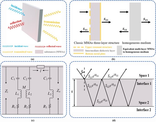
2.2.3. Transmission line theory
Based on the equivalent circuit method [Citation116,Citation117], researchers have proposed the transmission line theory to elucidate the absorption mechanism of MMAs. When electromagnetic waves are incident on MMAs, an equivalent transmission line model is established ((c)). Multilayer structures can be analyzed through the cascading method, and the dielectric layer or air layer is treated equivalent to transmission lines. Meanwhile, the coupling between layers is represented by mutual inductance and capacitance, and the ohmic loss and dielectric loss are approximated by the resistance of the circuit model.
Specifically, is the input impedance of the MMAs,
is the output impedance of the MMAs,
,
,
correspond to the electromagnetic resonance parameters of the top metal resonant structures in the equivalent circuit,
,
,
correspond to the dipole resonance parameters,
is the electromagnetic coupling parameter between these two resonances, and
,
,
correspond to the resonance parameters of the bottom metal structures in the equivalent circuit.
The transmission matrices of the top metal structure, dielectric layer, and bottom metal structure of MMAs are represented as follows:
where
,
is the electromagnetic wave vector, and
and
are the thickness and characteristic impedance of the dielectric layer, respectively. The transmission matrix of the entire MMAs is given by
The
-parameter matrix of MMAs is given by
The absorptivity can be simplified to
The transmission line theory regards the intermediate dielectric layer of MMAs as part of the transmission line model. It enables us to tune the impedance of MMAs by adjusting the thickness of the intermediate dielectric layer, thereby matching the equivalent impedance of free space and achieving perfect absorption.
Xu et al. designed and fabricated a triple band polarisation-sensitive wide angle MMA based on the transmission line theory [Citation114]. (b) shows the three-layer structure of this MMA, consisting of a resonant unit layer, a dielectric layer, and a metal substrate layer. The equivalent circuit model is also provided. The series of LC resonant units in the equivalent circuit diagram explain the electrical and magnetic resonances located in several absorption bands. By adjusting the equivalent LC value of the resonant unit, an absorber with arbitrary absorption frequency can be designed. By appropriately designing the structure of the surface resonant unit, intermediate dielectric layer, and metal substrate layer, the electrical and magnetic resonance can be modulated to coincide at the same frequency, thereby matching the impedance of the absorber with free space to achieve perfect absorption.
2.2.4. Interference theory
In 2012, Chen et al. proposed the multiple reflection interference theory to explicate a possible loss mechanism of electromagnetic waves in MMAs [Citation118]. The theory states that if the reflected and refracted electromagnetic waves destructively interfere with the incident electromagnetic waves, the MMAs can be considered perfect absorbers [Citation119,Citation120].
When electromagnetic waves are incident on MMAs, reflection and transmission occur at the interface [Citation121] ((d)). The reflection coefficient of the top layer is set to , and the transmission coefficient of the top layer is set to
. The electromagnetic waves at Interface 1 pass through the dielectric layer and reach the bottom metal structure. At this stage, the phase of the propagation waves increases by
, and all electromagnetic waves at the bottom of Interface 2 are reflected. The reflected electromagnetic waves propagate back to Interface 1, and the phase of the propagation waves increases by another
. Consequently, the electromagnetic wave undergoes reflection and transmission again with reflection and transmission coefficients of
and
, respectively. Therefore, the total electromagnetic wave in Space 1 is the superposition of multiple waves reflected by the MMAs, which can be expressed as
where
,
,
, and
are the reflection and transmission parameters at Interface 1,
is the reflection parameter at Interface 2,
is the propagation phase in the medium layer, and k and d are the propagation wave number and distance in the dielectric layer. The expressions for
and
are given by
In the scenario shown in (d), Space 1 represents air, and
represent the relative dielectric constant and magnetic permeability of air, respectively. Space 2 is the dielectric layer,
and
are the relative dielectric constant and magnetic permeability of the dielectric layer, respectively. Usually, the dielectric layer is composed of certain common dielectric materials, such as FR-4, with a relative magnetic permeability close to 1. Resulting in
. When incident vertically, the angle of incidence
, whereby the phase angle
is expressed as
If Interface 2 is a continuous metal film, electromagnetic waves cannot be transmitted (i.e.
). As a result,
To achieve perfect absorption (i.e.
), both the amplitude and phase must simultaneously meet the following criteria for total destructive interference
where
,
By designing unit cell structures and optimising the thickness of dielectric layers, the amplitude and phase can meet the conditions above simultaneously, leading to the maximal absorptivity of the MMAs
This process occurs in the intermediate dielectric layer of MMAs, as this theory focuses on the absorption and loss of electromagnetic waves in the intermediate dielectric layer.
Zeng et al. designed a three-band MMA based on the interference theory, quantitatively revealing the basic physical properties of absorption [Citation115]. (c) shows the multiple reflection interference model of the MMA, including two interfaces−the top air dielectric interface and the bottom dielectric-backplane interface. For the convenience of analysis, the thickness of these two interfaces was ignored. Electromagnetic waves underwent multiple reflections and transmissions within the MMAs, and multiple reflections were superimposed at the topmost interface. The peak absorption frequencies calculated based on the interference theory were located at 4.4, 6.05, and 13.9 GHz, consistent with simulation results.
2.3. Comparison of absorption mechanisms
Unlike traditional absorbing materials, electromagnetic MMAs, as a new type of absorbing material, can achieve flexible control of frequency, polarisation, amplitude, and phase characteristics of electromagnetic waves. In summary, traditional absorbing materials place more emphasis on the inherent physical properties of the material itself, which are usually difficult to change modulate. In contrast, MMAs centre on the design of structure, material, and arrangement of unit cells, which altogether set their electromagnetic parameters for electromagnetic wave absorption.
The aforementioned theories of MMAs applicable in different scenarios. Electromagnetic parameter inversion theory simplifies the multi-layer MMAs into a homogeneous medium for subsequent analysis. With measured reflection and transmission of MMAs, key parameters, such as dielectric constant, magnetic permeability, refractive index, and loss tangent, can be obtained through this theory. The impedance matching theory, as a widely accepted mechanism for electromagnetic wave absorption, can be applied to both traditional absorbing materials and MMAs. When the equivalent input impedance of MMAs matches that of free space, electromagnetic waves completely enter the absorber without undergoing reflection. This theory is more suitable for inverting and inferring the impedance matching relationship from simulation or test results, using the parameter to calculate the relative impedance of the absorber, checking its degree of impedance matching with air, and thus explaining absorption phenomena. However, it is extremely challenging to directly calculate the absorption frequency band from the intrinsic impedance distribution of MMAs. Particularly, it is difficult to accurately calculate the characteristic impedance when the structure is too complex to be made equivalent to a circuit model. The transmission line theory guides the design of MMAs with desirable absorption characteristics through L, C, R values. This theory is derived on the basis of equivalent circuit models and treats the intermediate dielectric layer of MMAs as part of the transmission line, which is often applicable to two-dimensional metasurface structures or relatively simple periodic unit structures of MMAs. This model enables easy derivation of key component parameters such as coupled inductors and capacitors, leading to optimised design and shortened design cycle. Interference theory can be used to analyze the absorption performance of MMAs in a quantitative way, capable of explaining the behaviours of MMAs with complex structures and electromagnetic waves with obliquely incident angles. Furthermore, this theory is not limited by frequency, covering a wideband ranging from radio frequency to microwave, and even infrared and visible light bands. Interference theory is applicable when there exists a difference in electromagnetic wave path, resulting in superposition and attenuation of waves. This condition often imposes certain requirements on the thickness and attenuation characteristics of the dielectric layer.
3. Manufacturing of electromagnetic MMAs by 3D printing
Traditional manufacturing techniques applied to fabricating electromagnetic MMAs encompass printed circuit boards [Citation122,Citation123], photolithography [Citation124,Citation125], magnetron sputtering [Citation126,Citation127], chemical vapour deposition [Citation128,Citation129], and micro/nano mechanical processing [Citation130]. However, these methods encounter inherent limitations. Firstly, these methods are primarily developed to manufacture 2D metasurface and face significant challenges in fabricating MMAs with intricate 3D structures and unit cell configurations. Secondly, many of these techniques exhibit compatibility constraints with specific types of substrate materials, thereby severely restricting material options for MMAs. In contrast, 3D printing, due to its unique freeform fabrication capability and benefits in structural design and material versatility, can mitigate the drawbacks associated with traditional manufacturing processes. The International Additive Manufacturing Technical Committee has delineated seven main additive manufacturing processes [Citation131,Citation132], three of which have been extensively utilised to fabricating MMAs, namely material extrusion, vat photopolymerization, and powder bed fusion. and summarises and compares representative MMAs manufactured by these three 3D printing processes and compares their materials and performance metrics.
Figure 4. The design and production process of 3D-printed MMAs. (a) Simulation includes structure, materials, and calculated parameters. (b) Typical 3D printing processes of MMAs [Citation96], copyright 2023, Springer Nature. (c) The post-processing summarised in this article. (d) Experimental schematic diagram in microwave bands [Citation147], copyright 2018, Elsevier, and terahertz bands [Citation148], copyright 2023, MDPI. (e) The comparison between one-step and two-step manufacturing.
![Figure 4. The design and production process of 3D-printed MMAs. (a) Simulation includes structure, materials, and calculated parameters. (b) Typical 3D printing processes of MMAs [Citation96], copyright 2023, Springer Nature. (c) The post-processing summarised in this article. (d) Experimental schematic diagram in microwave bands [Citation147], copyright 2018, Elsevier, and terahertz bands [Citation148], copyright 2023, MDPI. (e) The comparison between one-step and two-step manufacturing.](/cms/asset/75ea0ef4-242e-463c-b80d-135b71b15545/nvpp_a_2378937_f0004_oc.jpg)
Table 2. Comparison of reported MMAs manufactured via 3D printing including their designs and electromagnetic absorption performance.
3.1. One-step manufacturing of MMAs by 3D printing
In this context, one-step manufacturing through 3D printing means the process of creating MMAs that solely involves 3D printing along with basic post-curing, support removal, and sintering procedures, without the need for additional post-processing. MMAs manufactured via one-step 3D printing typically comprise all-dielectric structures, departing from the classical ‘metal–dielectric-metal’ structures. On the one hand, the simultaneous production of high-quality metal and dielectric structures through multi-process and multi-material 3D printing still presents significant challenges. On the other hand, all-metal structures manufactured by 3D printing generally exhibit relatively inferior surface quality and low printing resolution. Additionally, in all-metal-based MMAs, upon reaching the resonant frequency, the excitation of surface plasmon polariton leads to saturation of magnetic response, resulting in reduced absorption at higher frequencies [Citation149]. The combined advantages of all-dielectric MMAs and 3D printing result in a diverse range of innovative MMA designs capable of achieving broadband absorption while overcoming certain shortcomings associated with metal structures, such as vulnerability, high ohmic loss, and susceptibility to chemical erosion [Citation150–152]. Subsequent sections will elucidate how 3D printing technologies facilitate the one-step manufacturing of MMAs.
3.1.1. One-step manufacturing of MMAs by material extrusion
Material extrusion is a 3D printing process with molten materials extruded from nozzles and deposited layer by layer to form a 3D structure, which typically use thermoplastic filaments or shear-thinning solution/suspension as the raw materials. Fused Deposition Modeling (FDM), also known as Fused Filament Fabrication (FFF), and Direct Ink Writing (DIW) are examples of this category.
Numerous all-dielectric MMAs have been successfully manufactured in a single step using extrusion-based 3D printing. Chen et al. designed an all-dielectric and multi-band MMA by rotating an ‘I’-shaped beam to form the unit cell structure. This MMA, fabricated with Acrylonitrile Butadiene Styrene (ABS) through FDM, demonstrated five resonance peaks less than −10 dB across the band from 2 to 12 GHz [Citation133] ((a)). Similarly, Lim et al. developed a dual-function broadband MMA with electromagnetic wave absorption exceeding 90% for frequencies across the 5.8–18 GHz band. Furthermore, its octet-truss unit cell, 3D printed via FMD with a 20% carbon black-reinforced polylactic acid (PLA) composite filament [Citation134], enhanced the relative stiffness of the MMA ((b)). Based on the antenna reciprocity theory, Tan et al. 3D printed a propeller-like MMA via FDM in a single step, achieving absorptivity over 80% from 3.1 to 10.8 GHz [Citation153]. This MMA, benefiting from multiple resonance modes and tailored lossy materials, exhibited low profile, broadband, and wide-angle absorption ((c)). Furthermore, Yin et al. designed a multilayer MMA with a characteristic impedance gradient for impedance matching and efficient attenuation [Citation154]. In this design, composite materials with controllable characteristic impedance were utilised to 3D print this MMA via FDM, achieving over 90% absorptivity in the broadband ranging from 4.5 to 40 GHz by adjusting the graphene oxide content and architectural parameters of the unit cell ((d)). Li et al. proposed a 3D-printed terahertz broadband MMA featuring simple all-dielectric periodic resonance structures with transparent PLA as the dielectric material 3D printed by FDM. Because of the superposition of grating mode and waveguide resonance mode, this MMA exhibited broadband absorption characteristics from 0.31 THz to 1.0 THz keeping over 80% absorptivity and reaching a maximal absorbance of 99.8% at 0.48 THz [Citation155] ((e)).
Figure 5. Typical 3D-printed MMAs in one-step manufacturing through FDM, featuring their unit structure, overall structure, and electromagnetic absorption performance. MMAs with (a) rotating ‘I’-shaped structures, [Citation133], copyright 2023, Springer Nature. (b) geometrically optimised octet-truss structures, [Citation134], copyright 2022, Elsevier. (c) propeller-like structures, [Citation153], copyright 2023, Elsevier. (d) a gradient index (GRIN) of impedance [Citation154], copyright 2019, Elsevier. and (e) an ultra-broadband and transparent terahertz MMA [Citation155], copyright 2023, Elsevier.
![Figure 5. Typical 3D-printed MMAs in one-step manufacturing through FDM, featuring their unit structure, overall structure, and electromagnetic absorption performance. MMAs with (a) rotating ‘I’-shaped structures, [Citation133], copyright 2023, Springer Nature. (b) geometrically optimised octet-truss structures, [Citation134], copyright 2022, Elsevier. (c) propeller-like structures, [Citation153], copyright 2023, Elsevier. (d) a gradient index (GRIN) of impedance [Citation154], copyright 2019, Elsevier. and (e) an ultra-broadband and transparent terahertz MMA [Citation155], copyright 2023, Elsevier.](/cms/asset/bc4b3228-f5c0-4c45-8f7c-c656d598275c/nvpp_a_2378937_f0005_oc.jpg)
Unlike thermoplastic materials utilised in FDM, DIW typically prints viscoelastic materials exhibiting pronounced shear-thinning behaviour and high yield stress. For instance, Zhang et al. 3D-printed an asymmetric woodpile MMA via DIW-based one-step 3D printing, which overcame the local impedance mismatch and demonstrated a wider bandwidth compared to a simple tetragonal woodpile ((a)). The formulated DIW inks incorporated two loss fillers− carbon black and carbonyl iron powder. These MMAs achieved −10 dB absorption within the frequency band ranging from 3.9 to 18 GHz with the maximal reflection loss reaching −39 dB [Citation136]. Li et al. theoretically and experimentally proved that the electromagnetic absorption performance is significantly improved through better impedance matching when the carbonyl-iron/graphene is dispersed in the polymer substrate with a continuous concentration gradient. These MMA, manufactured in a single step via dual gradient DIW 3D printing, achieved a minimal reflection loss of −46.47 dB and an absorption bandwidth of 14.62 GHz [Citation137] ((b)). Moreover, the gradient lattice design effectively increased wave reflections in internal propagation, thereby enhancing electromagnetic attenuation. The DIW-based 3D printing process effectively integrates multiple absorbing fillers. Furthermore, the ink properties can be easily modulated by adjusting the ratio of raw materials, offering greater flexibility than other material extrusion-based 3D printing technologies and thus enhancing the electromagnetic wave absorption performance of MMAs.
Figure 6. Typical 3D-printed MMAs in one-step manufacturing through DIW, featuring their unit structure, overall structure, and electromagnetic absorption performance. MMAs with (a) asymmetric woodpile structures, [Citation136], copyright 2023, John Wiley and Sons. (b) gradient lattice structures. [Citation137], copyright 2022, Elsevier. Typical 3D-printed MMAs in one-step manufacturing through DLP or SLA. (c) twisted cross metamaterial structures [Citation140], copyright 2021, Elsevier. MMAs with (d) cross-helix array structures [Citation139], copyright 2022, Springer Nature, And (e) A new type of MMA with excellent comprehensive performance manufactured utilising electromagnetic adjustable polymer-derived ceramics. [Citation138], copyright 2023, Elsevier.
![Figure 6. Typical 3D-printed MMAs in one-step manufacturing through DIW, featuring their unit structure, overall structure, and electromagnetic absorption performance. MMAs with (a) asymmetric woodpile structures, [Citation136], copyright 2023, John Wiley and Sons. (b) gradient lattice structures. [Citation137], copyright 2022, Elsevier. Typical 3D-printed MMAs in one-step manufacturing through DLP or SLA. (c) twisted cross metamaterial structures [Citation140], copyright 2021, Elsevier. MMAs with (d) cross-helix array structures [Citation139], copyright 2022, Springer Nature, And (e) A new type of MMA with excellent comprehensive performance manufactured utilising electromagnetic adjustable polymer-derived ceramics. [Citation138], copyright 2023, Elsevier.](/cms/asset/da455a3a-3c2d-451d-a983-900d72d0a591/nvpp_a_2378937_f0006_oc.jpg)
The MMAs discussed above are manufactured by material extrusion-based 3D printing technologies, such as FDM and DIW, in a single step. As summarised in , the dimensions of their unit cell structures are typically on the millimetre scale and their minimum feature size reach several hundred micrometers. Ultimately, their electromagnetic wave absorption performance is modulated through the deliberate design of unit cell structures and material doping. However, the noticeable stair-stepping effect inherent to extrusion-based 3D printing may result in suboptimal surface quality, rendering it ill-suited for fabricating MMAs requiring high precision or intricate 3D structures. Furthermore, the relatively low printing resolution imposes significant limitations on the feature size of the unit cell. Consequently, MMAs 3D printed via material extrusion typically operate in the microwave band and are unsuitable for high-frequency bands due to the adverse effect caused by rough surface texture and large feature size on the absorption of high-frequency electromagnetic waves [Citation156].
3.1.2. One-step manufacturing of MMAs by vat photopolymerization (VPP)
VPP is a high-precision 3D printing process relying on photosensitive materials. This method typically employs ultraviolet light sources to selectively expose photosensitive resins, allowing them to solidify into specific patterns and stack layer by layer into 3D objects. Digital Light Processing (DLP), Stereo Lithography Appearance (SLA), and Two-Photon Polymerization (2PP) belong to the VPP category, all of which are extensively used in the manufacturing of photosensitive resin-based MMAs. Moreover, precursor-derived ceramics promise great potential for the manufacturing of high-temperature devices with broadband absorption capability[Citation157–160]. By incorporating ceramic powder fillers into photosensitive resin or by employing the precursor-derived ceramic process [Citation161,Citation162], ceramic MMAs with strong mechanical properties and outstanding absorption performance can be readily fabricated by VPP.
Based on the theory discussed in Chapter 2, Hui et al. prepared an Al2O3/carbon nanotubes/SiC nanowires/SiOC composite using the precursor infiltration pyrolysis method and 3D printed it into a MMA with twisted cross structures via SLA. The dielectric and conductive losses of the MMA made from this composite material were significantly improved, and the absorption bandwidth was able to cover the entire X-band [Citation140] ((c)). In another study, Zhou et al. presented a light-curable polysiloxane precursor for the manufacturing of Si-O–C ceramic MMAs composed of unique cross-helix unit cell structures via DLP 3D printing. These MMAs exhibited a minimal reflection loss value of −56.11 dB and absorption within the bandwidth ranging from 9.27 to 12.4 GHz ((d)) [Citation139]. Furthermore, the peak absorption could be extended to other frequency bands by adjusting the unit cell structure, providing a novel and effective approach of developing ceramic-based MMAs with micro and nano-scale structures. Yao et al. proposed a top-down parametric design methodology for the manufacturing of high-temperature MMAs through DLP 3D printing by utilising electromagnetic adjustable polymer-derived ceramics ((e)) [Citation138]. At room temperature, the proposed MMAs exhibited a minimal reflection loss of −58.05 dB with an effective absorption bandwidth reaching 6.11 GHz. Subsequently, the thermal response of the MMAs was investigated, revealing an increase in minimal reflection loss value to −72.38 dB at 100°C and a bandwidth extension to 6.77 GHz at 300°C. In addition, Lu et al. successfully utilised DLP to prepare two high-temperature resistant ceramic-based 3D-printed MMAs with broadband absorption [Citation163,Citation164]. One of the works fabricated three new non-resonant SiOC-based MMAs with triply periodic minimal surface (TPMS) meta-structures, and the other designed an ultraviolet (UV)-curable polysiloxane (PSO) resin slurry for the preparation of gyroid structures ceramic MMAs. On the material side, the aforementioned works either prepared precursor-derived ceramics (PDCs) or PSO resin slurry as the raw printing material. However, the final solid content and dopants are different which are tuned with the aim to optimise impedance matching and loss characteristics. In terms of process, they all utilise DLP to 3D print MMAs followed by post treatment with precursor infiltration and pyrolysis (PIP) method. However, different temperature profiles are employed for pyrolysis. The structure of unit cells transforms from twisted cross and cross array to intricate TPMS and multi-layer gradient designs. Through material, process, and design optimisation, ceramic-based MMAs have shown significantly improved performance, including minimum reflection loss, large absorption bandwidth, strong mechanical properties, and high temperature resistance.
A thorough examination of the aforementioned MMAs highlights the significant enhancement in absorption and mechanical properties accomplished through VPP. This improvement is primarily attributed to the incorporation of composite materials with varying filler ratios and intricate designs of lattice or porous structures. As summarised in , VPP stands out as one of the most accurate 3D printing technologies with fine features and high-quality surfaces, rendering it particularly well-suited for applications requiring intricate structures, small feature sizes, and high printing precision. VPP empowers direct and one-step fabrication of micro/nanostructures, thereby overcoming the limitations of extrusion-based 3D printing, such as low printing resolution and poor surface quality. The working frequency of MMAs fabricated by VPP reach the microwave, terahertz, or even near-infrared bands, with corresponding minimal feature sizes ranging from millimetres to micrometers, and even nanometres. Consequently, VPP presents a superior solution for the design and production of MMAs tailored to operate in higher frequency bands.
3.1.3. One-step manufacturing of MMAs by powder bed fusion (PBF)
PBF constitutes an additive manufacturing process wherein thermal energy selectively melts powder (e.g. plastic, metal, or ceramic) within the construction area to create solid objects layer by layer. The powder material is evenly spread into thin layers on the printing bed, and energy supplied by the laser or electron beam is directed to fuse powders in the designated area into a solid block on the powder bed. Subsequently, another powder layer is spread evenly to cover the previous layer, iteratively repeating the process to complete the whole object [Citation165–168]. Selective Laser Melting (SLM), Selective Laser Sintering (SLS), and Electron Beam Melting (EBM) all fall under this category.
Polyamide (PA) stands out as one of the most prevalent powder materials utilised in PBF 3D printing. Numerous MMAs fabricated via PBF utilise PA-based composite materials such as PA/silicon carbide, PA/aluminum [Citation169], and PA/carbon fibre [Citation170–172]. For instance, Zhou et al. 3D printed a multilayered broadband radar MMA comprising a mixture of nylon and carbonyl iron powders using SLS [Citation146]. The absorption characteristics, theoretically calculated and simulated, were validated by experimental measurements, consistently demonstrating reflection loss values of less than −10 dB across the 8–18 GHz frequency band. In another study, Gong et al. successfully 3D printed a MMA with flexible honeycomb unit structures using a composite comprising carbon fibre, polyamide, and carbonyl iron via SLS in a single step ((a)) [Citation173]. They explored three different unit cell structures and discovered that the porous semi-solid honeycomb structure exhibited the best performance of electromagnetic absorption, achieving a minimal reflection loss of −16.8 dB and an effective absorption bandwidth value of 2.4 GHz in an unbending state. Wen et al. utilised PA 12-coated carbonyl iron powder to 3D print high-performance MMAs via SLS. The MMAs in this study exhibited reflection loss values of less than −10 dB within the range of 2.7–18 GHz [Citation143]. Mechanical testing proved that the MMAs infiltrated with thermosetting epoxy resin (EP, e44) exhibited improved relative density and strength, thereby significantly enhancing their tensile strength ((b)).
Figure 7. Typical 3D-printed MMAs in one-step manufacturing through SLS, featuring their unit structure, overall design, and electromagnetic absorption performance. (a) A new flexible honeycomb MMA. [Citation173], copyright 2021, Elsevier. (b) A three-dimensional MMA with complex structure and high absorption performance. [Citation143], copyright 2020, Elsevier. Typical 3D-printed MMAs manufactured in two-step with post processing by surface metallization, featuring their unit structure, overall design, electromagnetic absorption performance, and process procedures. (c) A cross-shaped terahertz MMA. The cross-shaped array is first 3D printed followed by electron beam evaporation deposition of a gold film. [Citation190], copyright 2021, Elsevier. (d) A tower-shaped terahertz MMA stacked on disks, The tower structure is first 3D printed followed by magnetron sputtering on a gold film. [Citation191], copyright 2021, American Physical Society.
![Figure 7. Typical 3D-printed MMAs in one-step manufacturing through SLS, featuring their unit structure, overall design, and electromagnetic absorption performance. (a) A new flexible honeycomb MMA. [Citation173], copyright 2021, Elsevier. (b) A three-dimensional MMA with complex structure and high absorption performance. [Citation143], copyright 2020, Elsevier. Typical 3D-printed MMAs manufactured in two-step with post processing by surface metallization, featuring their unit structure, overall design, electromagnetic absorption performance, and process procedures. (c) A cross-shaped terahertz MMA. The cross-shaped array is first 3D printed followed by electron beam evaporation deposition of a gold film. [Citation190], copyright 2021, Elsevier. (d) A tower-shaped terahertz MMA stacked on disks, The tower structure is first 3D printed followed by magnetron sputtering on a gold film. [Citation191], copyright 2021, American Physical Society.](/cms/asset/39d959ab-3fce-4b3e-916a-9d8b5d128dac/nvpp_a_2378937_f0007_oc.jpg)
shows that the resolution and accuracy of PFB and material extrusion-based 3D printing are roughly the same, and the minimum feature size (in the hundreds of micrometers level) and working frequency band of the manufactured MMAs are also similar. The MMAs 3D printed by PBF generally exhibit superior mechanical properties compared to other 3D printing methods, which is attributed to the high-temperature or high-power process involved in PBF, resulting in dense parts with low porosity. Furthermore, the powder bed itself could provide sufficient support for suspended structures, thus eliminating the need for additional support structures. Despite these advantages, the relatively high maintenance requirements and complicated operations associated with PBF significantly limit its widespread adoption in MMA fabrication. Moreover, the size of powder particles used in PBF is relatively large, typically falling within the range of several tens of microns to ensure good spreadability, which poses a significant limitation on the printing solutions and makes them unsuitable for the fabrication of MMAs with fine features designed to operate in high-frequency bands.
3.2. Two-step manufacturing of MMAs by 3D printing
Although manufacturing MMAs by one-step 3D printing offers advantages such as low cost, fast speed, and simple process, the one-step process often faces limitations in material selection, typically restricted to a single material or a homogeneous composite. However, many MMAs, particularly those with classic ‘metal–dielectric-metal’ structures [Citation174], entail multiple materials and fabrication processes in order to achieve specific absorption characteristics [Citation175,Citation176]. Compared to metals, a more diverse range of dielectric materials are compatible with 3D printing processes. By depositing metal layers onto 3D-printed dielectric substrates post-printing, 3D MMAs with intricate structures can be created with great ease and flexibility, no longer confined to 2D metal structures. Meanwhile, new structural materials and media with distinctive absorption characteristics, such as water [Citation177,Citation178], graphene [Citation179–182], carbon nanotubes [Citation183–185], and carbon black [Citation186–188], have been discovered and applied to MMAs. Incorporating these materials into MMAs has led to improved absorption performance primarily through two approaches: one by doping these materials into the polymer or resin and the other by infusing these substances into the cavity of 3D-printed hollow MMAs. Traditional manufacturing processes often face challenges in realising cavities and microchannels, a limitation that is easily circumvented with the assistance of 3D printing [Citation189]. In this article, various two-step 3D printing processes commonly employed to fabricate MMAs are discussed. These processes are broadly categorised into surface and internal post-processing approaches.
3.2.1. Post processing by surface metallization
Gold (Au), silver (Ag), and copper (Cu) are commonly used precious metal materials for the metal-based electromagnetic wave absorbing materials [Citation190,Citation192,Citation193]. In addition, alloys [Citation194] and metal oxides [Citation195,Citation196] are also frequently utilised in traditional metal-based electromagnetic wave absorbers. In a typical three-layer MMA, impedance can be modulated by designing a top metal resonant structure and a bottom metal plate to match the impedance of MMA to that of free space. At the same time, the antiparallel current induced by the upper and lower metal layers generates a magnetic response, further amplifying electromagnetic resonance and enhancing electromagnetic wave absorption. Therefore, research on metal–dielectric-based MMAs is crucial, and numerous successful examples of MMAs fabricated by two-step manufacturing processes that combine 3D printing and surface metallization techniques have emerged.
3.2.1.1. Metallization by surface coating
Magnetron sputtering and electron beam evaporation are two most common micro and nano coating processes employed to prepare thin metal films [Citation197–200]. They enable two-step manufacturing of MMAs when used in combination with high-precision 3D printing technologies. For instance, Li et al. proposed a MMA with vertical split-ring resonators, manufactured by 3D printing dielectric resin structures with DLP followed by depositing a copper film via magnetron sputtering [Citation201]. The centrally unsymmetrical structure of the MMA resulted in an absorption peak at 0.8 THz only under x-polarisation, not under y-polarisation. This work demonstrated the potential of combining 3D printing with surface metallization for manufacturing terahertz MMAs. Subsequently, Li et al. proposed a typical cross-shaped single-band MMA manufactured by 3D printing the dielectric resin structure via DLP followed by gold coating with electron beam evaporation [Citation202] ((c)). By arranging cross-shaped unit cell structures of varying sizes horizontally, multiple resonant peaks were superimposed, resulting in significantly broadened absorption bandwidth. Through this structural transformation, the absorption peak at 0.94 THz was transformed into broadband absorption ranging from 0.659 THz to 0.802 THz. Furthermore, Shen et al. reported a stereoscopic multilayered ultra-broadband terahertz MMA by stacking multilayers of concentric resonators into a monolithic 3D pagoda-like structure manufactured via DLP 3D printing followed by electron-beam deposition. By stacking disks of various sizes vertically, resonance absorption peaks were superimposed into an ultrabroad absorption band ranging from 0.41 to 1.60 THz [Citation191] ((d)). Sadeqi et al. combined SLA and surface metal coating to manufacture MMAs. They innovatively proposed mushroom-shaped MMAs and omni-directional hemispherical moth-eye MMAs to tune the operating frequency into the millimetre wave band. Surface metallization was applied either by dip coating or sputtering [Citation203].
While metal coating technology, such as magnetron sputtering and electron beam deposition, are widely used in the semiconductor industry for thin film production and research, their integration with high-precision 3D printing facilitates the creation of MMAs with intricate 3D dielectric–metal structures. However, the thin film metal coating is limited to specific types of substrate materials with strong adhesion to metals and may not be suitable for manufacturing large-sized devices. Nevertheless, when utilised in conjunction, these processes are well-suited for the fabrication of MMAs designed to operate within the spectra of millimetre wave, terahertz, and other high-frequency electromagnetic waves. In the frequency bands mentioned above, the minimal feature size of MMAs typically ranges from micrometers or hundreds of nanometres. VPP-based 3D printing technology is the most well-suited solution to meet such requirements for high precision and resolution.
3.2.1.2. Metallization by surface spraying or printing
Unlike magnetron sputtering and electron beam evaporation deposition, which entail high-maintenance equipment and a tedious workflow, surface spraying or printing provides a more straightforward way of preparing metal layers on 3D-printed structures. These methods can either deposit a confluent coating or a patterned layer through silkscreens or other types of stencils on 3D-printed structures. For instance, Lim et al. designed a MMA with staired Jerusalem cross (JC) structures, which was manufactured by 3D printing dielectric structures using FDM. Subsequently, a conductive metal layer was deposited onto the 3D-printed dielectric structure by spraying silver paste. The absorptivity of this MMA exceeded 99% at 5.18 GHz [Citation204]. Similarly, Ghosh et al. 3D printed a broadband MMA comprising a periodic array of dielectric honeycomb cores. Using screen printing technology, resistive ink was patterned onto the FDM-printed dielectric structure [Citation205]. Kim et al. proposed a double-layer MMA with a conductive swastika symbol as the top pattern. This device was two-step manufactured by 3D printing the structure via FMD and painting the conductive pattern with silver ink ((a)). The simulated and measured absorptivity of this MMA reached above 90% at 1.91 GHz [Citation206]. Yoon et al. proposed a MMA composed of a periodic unit cell structure with a truncated cone. This device was 3D printed with PLA filament using FDM and metalised by spraying conductive paste containing silver-coated copper particles. When electromagnetic waves were incident normally onto the MMA, the absorptivity exceeded 90% at 10.81 GHz with a broadband absorption ranging from 5.52 to 16.96 GHz under normal incidence [Citation207] ((b)). Furthermore, it demonstrated good mechanical strength and lightweight characteristics because of its perforated architecture.
Figure 8. Typical 3D-printed MMAs in two-step manufacturing followed by post processing by surface spraying or printing, featuring their unit structure, overall design, electromagnetic absorption performance, and process procedures. (a) A double-layer MMA with a conductive swastika symbol painted with silver ink. [Citation206], copyright 2020, John Wiley and Sons. (b) A periodic unit cell structure with a truncated cone metalised by spraying conductive paste. Typical 3D-printed MMAs in two-step manufacturing followed by post processing by thin foil lamination. [Citation204], copyright 2018, John Wiley and Sons. (c) A 3D-printed honeycomb structure stacked on top of a piece of 1-mm thick copper foil. [Citation208], copyright 2018, Springer Nature. (d) An ultra-broadband microwave MMA based on dielectric resonant cavities with a copper foil of 0.1 mm attached to the back of the dielectric plate. [Citation209], copyright 2018, MDPI. (e) A lightweight broadband MMA with a copper foil adhered to the lower surfaces. [Citation210], copyright 2021, Elsevier.
![Figure 8. Typical 3D-printed MMAs in two-step manufacturing followed by post processing by surface spraying or printing, featuring their unit structure, overall design, electromagnetic absorption performance, and process procedures. (a) A double-layer MMA with a conductive swastika symbol painted with silver ink. [Citation206], copyright 2020, John Wiley and Sons. (b) A periodic unit cell structure with a truncated cone metalised by spraying conductive paste. Typical 3D-printed MMAs in two-step manufacturing followed by post processing by thin foil lamination. [Citation204], copyright 2018, John Wiley and Sons. (c) A 3D-printed honeycomb structure stacked on top of a piece of 1-mm thick copper foil. [Citation208], copyright 2018, Springer Nature. (d) An ultra-broadband microwave MMA based on dielectric resonant cavities with a copper foil of 0.1 mm attached to the back of the dielectric plate. [Citation209], copyright 2018, MDPI. (e) A lightweight broadband MMA with a copper foil adhered to the lower surfaces. [Citation210], copyright 2021, Elsevier.](/cms/asset/ff3a7f7e-6a6e-4f27-a5a6-7a2b685e8804/nvpp_a_2378937_f0008_oc.jpg)
The structural dimensions of aforementioned MMAs are relatively large compared to those fabricated by VPP-based 3D printing techniques because of the relatively inferior printing resolution of mainstream material extrusion-based 3D printing techniques. Moreover, compared to surface post-processing such as magnetron sputtering and electron beam evaporation, spraying and printing are more cost-effective and convenient. However, the metal layer obtained through spraying and printing is relatively rough, making them suitable only for MMAs operating in the microwave or other bands with even lower frequencies. The wavelength corresponding to these lower frequency ranges are relatively large, and the unit cell size of MMAs is located in the sub-wavelength size (millimetre level). These size requirements can meet using various 3D printing processes followed by convenient and cheap spraying and printing for metallization, without the need for refined micro/nano metal film making technology.
3.2.1.3. Metallization by thin foil lamination
Incorporating a layer of metal foil as the base of MMAs prevents electromagnetic waves from transmitting through the MMAs. Typically, the thickness of the metal foil exceeds the skin depth at the working frequency to ensure efficient absorption. The metal foil can be placed on the printing platform prior to printing, allowing MMA structures to be directly printed onto it. Alternatively, the metal foil can also be affixed to the bottom of MMAs after printing using various bonding methods. For instance, [Citation211] proposed a MMA with intricate perforated structures 3D printed with PLA [Citation211]. After 3D printing, a layer of anti-transmission copper foil was affixed to the bottom, resulting in a lightweight and structurally stable MMA feature by its small thickness and wide absorption band. Similarly, Jiang et al. reported a 3D MMA consisting of a 3D-printed PLA honeycomb, resistive patches, and a metallic backboard stacked on top of a piece of 1-mm thick copper foil ((c)). This MMA achieved over 90% absorptivity within the 3.53–24.00 GHz band for vertically incident electromagnetic waves [Citation208]. Furthermore, mechanical tests showed that this MMA demonstrated outstanding mechanical performance under substantial compressive loads. Furthermore, Ren et al. proposed an ultra-wideband microwave MMA based on a 3D-printed dielectric resonant cavity with a copper foil of 0.1 mm in thickness attached to the back of the dielectric plate [Citation209]. This MMA exhibited over 90% absorptivity across the entire C-band and X-band ((d)). Moreover, [Citation211] leveraged the strong mechanical strength of thermoplastic polyether-ether-ketone (PEEK) to create a lightweight broadband MMA with excellent electromagnetic absorption ability and mechanical properties [Citation210]. In this design, the intermediate dielectric layer was 3D-printed via FDM, and the Indium Tin Oxide (ITO) resonant pattern and copper foil were adhered to the upper and lower surfaces, respectively, using optical transparent adhesive. The absorptivity of this MMA exceeded 90% across the 5.7–19.85 GHz band, and the compressive strength of the compass-shaped PEEK substrate reached 22.45 MPa at 90°C, the same as that at room temperature ((e)).
From the perspective of 3D printing modalities, the aforementioned MMAs devices are all manufactured by material extrusion-based 3D printing, with their dielectric structure utilising PLA or ABS as raw materials. Affixing a layer of metal foil to the MMAs prevents the transmission of electromagnetic waves through the device, serving as an auxiliary way of enhancing absorption rather than constituting the main resonant structures. This metal foil is usually laminated onto the flat bottom surface instead of conforming to the 3D structures of the MMA device, making it relatively straightforward to implement compared to other metallization processes. The exact process to be selected for metal thin film coating depends on the size of the MMA and the required quality. If the size of the MMA is large and the required quality of the metal thin film is not high, simple lamination processes could meet the requirement. If the working frequency band is high and a high-quality metal surface is required, micro/nano coating processes, such as sputtering and e-beam evaporation, are often used to accomplish the goal.
3.2.2. Post processing by internal infusion
Departing from conventional solid-material-based MMAs, liquid-infused MMAs offer tunable absorption owing to their adaptable architecture [Citation212]. In contrast to metal-structured MMAs, the dispersion characteristics of the infused liquid typically result in a broader absorption bandwidth. Recently, 3D printing has been adopted to facilitate the fabrication of intricate inner cavities embedded in the MMAs to accommodate liquid infusion. Researchers have infused a diverse range of liquid materials with high electromagnetic loss characteristics into 3D-printed dielectric structures, thereby creating MMAs tailored for absorbing electromagnetic wave energy and offering versatile electromagnetic wave manipulation and control.
3.2.2.1. Water-infused 3D-printed MMAs
Water, with its high dielectric constant and loss characteristics, is an excellent electromagnetic wave absorbing material, particularly in the microwave band. It is therefore commonly used as the infusion liquid for MMAs. Initially, Yoo et al. proposed the first water-based MMA, employing a simple structure that relied on a hydrophilic and hydrophobic pattern By manipulating the amount of water to control the height and diameter of water droplets, the absorption bandwidth could be effectively modulated [Citation213]. However, this device was not fabricated by 3D printing. Since then, the development of water-infused MMAs has progressed rapidly, particularly through two-step manufacturing approaches wherein the solid hollow structure was 3D printed followed by liquid infusion into cavities and microchannels. For instance, Shen et al. designed a water-based MMA with multiple layers of irregular cavities sandwiched between the two dielectric resin layers, wherein the cavities were created with a photosensitive resin using a VPP-based 3D printing technique. This MMA achieved an ultra-broadband absorptivity over 90% in the band ranging from 6.8 to 21.0 GHz [Citation214]. Furthermore, Zhang et al. 3D-printed a water-based MMA with swastika-shaped cavities, demonstrating absorption over 90% within the frequency band ranging from 9.3 to 49.0 GHz and maintaining a stable electromagnetic absorption within a large range of incident angles. Moreover, the absorption showed almost no significant change as the water temperature rose from 0°C to 100°C [Citation215]. This MMA was manufactured using PLA through FDM 3D printing, with microchannels designed for easy water injection. Li et al. reported a water-based MMA with transparent cylindrical resonant cavities, manufactured through a two-step process involving VPP-based 3D printing and internal water infusion. This MMA exhibited absorptivity over 90% from 6.5 GHz to 21.4 GHz, maintaining polarisation insensitivity and effective absorption of both TE and TM waves when the incident angle was less than 45 °C [Citation216]. Moreover, Deng et al. presented a water-based MMA with cubic and cross-shaped cavities, achieving ultrabroad bandwidth absorption over 90% from 16.52 GHz to 100.00 GHz at incident angles less than 60 °C ((a)) [Citation217]. Similarly, this MMA also utilised VPP-based 3D printing to manufacture the shell and cavity structure followed by water infusion post processing. Similarly, Chen et al. proposed a water-based MMA 3D printed via FDM, showing an ultra-broadband absorptivity exceeding 90% from 9.6 to 98.9 GHz [Citation218] ((b)). During the printing process, absorbent calcium alginate hydrogel was injected first followed by water infusion in order to reduce bubble formation.
Figure 9. Typical 3D-printed MMAs in two-step manufacturing followed by post processing by internal water or ionic liquid infusion, featuring their unit structure, overall design, and electromagnetic absorption performance. (a) A water-based MMA with cubic and cross-shaped cavities. [Citation217], copyright 2022, Springer Nature. (b) An ultra-broadband water-based MMA with complex multilayer structures. [Citation218], copyright 2021, Optica Publishing Group. (c) An ultra-broadband ionic liquid-based MMA with cylindrical cavity structures. [Citation224], copyright 2017, Royal Soc Chemistry. (d) An all-dielectric ionic liquid-based MMA with annular cavity structures. [Citation225], copyright 2019, IOP Publishing.
![Figure 9. Typical 3D-printed MMAs in two-step manufacturing followed by post processing by internal water or ionic liquid infusion, featuring their unit structure, overall design, and electromagnetic absorption performance. (a) A water-based MMA with cubic and cross-shaped cavities. [Citation217], copyright 2022, Springer Nature. (b) An ultra-broadband water-based MMA with complex multilayer structures. [Citation218], copyright 2021, Optica Publishing Group. (c) An ultra-broadband ionic liquid-based MMA with cylindrical cavity structures. [Citation224], copyright 2017, Royal Soc Chemistry. (d) An all-dielectric ionic liquid-based MMA with annular cavity structures. [Citation225], copyright 2019, IOP Publishing.](/cms/asset/c761b88a-15a7-44bb-83d1-81aeae1b5d1d/nvpp_a_2378937_f0009_oc.jpg)
Water possesses desirable dielectric loss characteristics across a broad frequency range, rendering it a natural cost-effective material well-suited for creating broadband absorbers. Furthermore, its dielectric constant varies with temperature as per the Debye model, allowing for thermal modulation of MMAs. Therefore, the integration of intricate cavities fabricated by 3D printing and advantageous electromagnetic properties of water results in an easily accessible and cost-effective electromagnetic MMAs with great potential for pragmatic applications. According to earlier investigations, water-based MMAs often work in the microwave band. For them to operate in higher frequency, the dimension of cavities and microchannels must reach micrometer or nanometre levels. However, it is challenging to remove supporting structures required for 3D printing certain hollow structures at such small scales. Additionally, infusing such small channels also presents significant technical hurdles.
3.2.2.2. Ionic liquid-infused 3D-printed MMAs
Ionic liquids constitute a diverse category of dissolved salts composed solely of cations and anions [Citation219,Citation220]. They offer unique advantages for applications in MMAs due to their high-loss characteristics stemming from their high ionic conductivity and dielectric loss factor [Citation221,Citation222]. By varying the composition of cations and anions of ionic liquids, their dielectric properties can be finely tuned [Citation223], allowing for precise control of the MMAs’ performance. In contrast to water-based MMAs, ionic liquids-infused MMAs not only significantly broaden the absorption bandwidth but also exhibit exceptional thermal stability owing to the nature of ionic liquids. The dense pairs of anions and cations of ionic liquids lead to dielectric polarisation, generating ion currents that enhance electromagnetic losses.
Moreover, the performance of ionic liquid-infused MMAs remained relatively consistent as the water temperature varied from 0°C to 100°C, making them highly adaptable across various operating conditions. Gong et al. pioneered the strategy of infusing ionic liquids into cavities fabricated via VPP-based 3D printing, resulting in an ultra-broadband MMA with absorptivity over 90% across the 8.4–29.0 GHz frequency band [Citation224] ((c)). Subsequently, [Citation211] proposed an all-dielectric ultra-broadband MMA infused with imidazole ionic liquids, featuring an improved hollow annular groove structure fabricated via VPP-based 3D printing. This design facilitates impedance matching with free space [Citation225], achieving absorptivity over 90% across the 13.9–50 GHz frequency band and polarisation insensitivity for incident angles below 60° ((d)). Moreover, Zhang et al. and [Citation211] conducted a systematic investigation on ionic liquids-based MMAs. They engineered hollow ring structures of similar designs, fabricated by VPP-based 3D printing techniques, which were subsequently infused with ionic liquid and packaged [Citation226,Citation227]. Their experimental and simulation results showcased the excellent electromagnetic absorption performance of ionic liquid-based MMAs within the microwave band.
The findings of the research above underscore the efficacy of infusing ionic liquids in improving the impedance matching between MMAs and free space. In addition, the distinctive loss mechanism of ionic liquids in the microwave band imparts these MMAs with broadband absorption capability, surpassing the bandwidth of water-based counterparts while maintaining stability within a wide operating temperature range. Furthermore, ionic liquid-infused MMAs hold the potential to modulate electromagnetic wave absorption by altering the ion density and type.
3.2.2.3. Liquid metal-infused 3D-printed MMAs
Conventional metallization processes deposit metal layers on outer surfaces, posing challenges for creating intricate 3D metal structures, particularly in the interior of devices. Liquid metal, characterised by high conductivity and excellent fluidity at room temperature, enables rapid metal patterning through pressure-driven injection into 3D-printed fluidic confinement structures such as microchannels and cavities [Citation228]. Consequently, liquid metal serves as an excellent material for the resonant metal layer of tunable MMAs. Prior to the advent of 3D printing technologies, researchers employed various methods to fabricate liquid metal-based MMAs, such as computer numerical control (CNC) [Citation229], laser etching [Citation230], and conventional PCB manufacturing processes [Citation231]. 3D printing has significantly simplified the process. For instance, Kim et al. proposed a stretchable MMA by infusing eutectic gallium indium (EGaIn) liquid metal into 3D-printed polydimethylsiloxane (PDMS) microchannels, achieving absorptivity of 97.8% at 18.5 GHz ((a)). In this work, incorporating 3D printing for the fabrication of unit cell structures significantly reduces the fabrication time and complexity of workflow [Citation232]. Similarly, Liang et al. reported a tunable liquid metal-infused MMA composed of a 3D-printed dielectric unit cell fabricated using photosensitive resin by SLA, which possessed a square cavity loaded with liquid metal and four T-shaped microchannels used for connection ((b)). This MMA showed strong absorbance from 3.13 GHz to 10.45 GHz [Citation141]. In addition to liquid metal-based MMAs in the microwave band, Yin et al. created two terahertz liquid metal-based MMAs infused with gallium-indium-tin (GaInSn) using a high-precision DLP 3D printing process [Citation233]. One comprised multiple layers of disks with ultra-broadband absorption ranging from 2.2 to 3.0 THz, while the other featured orthogonally crossed vertical split rings with multiband absorption.
Figure 10. Typical 3D-printed MMAs manufactured in two-step followed by post processing by internal liquid metal infusion, featuring their unit structure, overall design, and electromagnetic absorption performance. (a) A stretchable liquid metal-based MMA by infusing EGaIn into 3D-printed PDMS microchannels. [Citation232], copyright 2016, MDPI. (b) A tunable liquid metal-based MMA with a square cavity and four T-shaped microchannels. [Citation141], copyright 2020, Springer Nature.
![Figure 10. Typical 3D-printed MMAs manufactured in two-step followed by post processing by internal liquid metal infusion, featuring their unit structure, overall design, and electromagnetic absorption performance. (a) A stretchable liquid metal-based MMA by infusing EGaIn into 3D-printed PDMS microchannels. [Citation232], copyright 2016, MDPI. (b) A tunable liquid metal-based MMA with a square cavity and four T-shaped microchannels. [Citation141], copyright 2020, Springer Nature.](/cms/asset/aadc18f6-cf1c-49e0-9a1b-a3e54945805d/nvpp_a_2378937_f0010_oc.jpg)
Compared to surface metallization process, the liquid metal infusion approach is robust and easy to implement. Owing to its inherent deformability, the metal structures of MMAs can be easily patterned. 3D printing technology offers unprecedented advantages in creating embedded 3D microchannels and cavities. The high printing resolution of VPP-based 3D printing technology is able to ensure micro or even nanoscale production of MMAs structures. Combined with microfluidic technology, it presents novel opportunities for the exploration of liquid metal-infused MMAs. summarises and compares the additive manufacturing methods and post-treatment techniques used for manufacturing MMAs.
Table 3. Comparison of additive manufacturing methods and post-processing technologies used to fabricate MMAs.
4. Tunable MMAs via 4D printing
4D printing represents a transformative advancement in additive manufacturing, extending traditional 3D printing into the fourth time dimension by creating objects pre-programmed to undergo a predicable transformation in shape or other properties over time upon specific stimulation, allowing them to adapt to the changing environment conditions [Citation234–237]. These smart objects created by 4D printing have already been widely used as adaptive medical implants, soft robotics, and self-assembled equipment, among other applications [Citation238–240]. The concept of 4D printing has also been extended to the field of tunable MMs such as 4D-printed mechanical MMs [Citation241–243], 4D-printed tunable electrical MMs [Citation244,Citation245] and 4D-printed shape memory MMs [Citation246–248]. By 3D printing transformable unit cells, the electromagnetic response of MMAs can be precisely modulated, greatly extending the applicability and versatility of 3D-printed MMAs. This section explores two approaches of accomplishing 4D transformation. The first approach involves the rearrangement of multiple components that form the MMAs, thereby modulating their electromagnetic characteristics. The second approach induces the shape morphing of soft MMAs upon stimulation, leading to dynamic changes in the electromagnetic characteristics of MMAs. Both 4D printing approaches represent innovative strategies for enhancing the performance of MMAs.
4.1. 4D-printed reconfigurable MMAs
Unlike conventional MMAs, which are typically monolithic, 4D-printed reconfigurable MMAs comprise of multiple bodies that can be arranged in various configurations. These 4D-printed multifunctional MMAs leverage innovative designs, achieving functionalities unattainable by conventional MMAs, such as controllable absorption, multi-band selective filtering, and electromagnetic shielding, by reprogramming magnetic response through structural reconfiguration. For instance, Chen et al. proposed a reconfigurable MMA employing liquid metal-infused 3D-printed cavities, allowing for reconfiguration of electromagnetic characteristics ((a)) [Citation249]. By stacking multiple C-shaped resonators, the MMA could dynamically adjust its absorption performance such as single and dual-band switches, three-band absorption, and intensity adjustment by mechanically rotating the relative orientation of the resonators, showcasing the versatility and adaptability of the reconfigurable MMA design. In another study by Jeong et al., a dielectric MMA with optical transparency was 3D printed using a VPP-based technique ((b)) [Citation250]. This MMA incorporates cavity structures to modulate the electromagnetic wave absorption and reflection based on the presence or absence of water infusion. When filled with water, the device acted as an absorber, achieving absorptivity over 90% from 5.3 to 15.2 GHz. Conversely, the device acted as a reflector in the absence of water, maintaining a reflection coefficient of less than −5 dB at the working frequency. Furthermore, inspired by the restructuring of mortise and tenon structures, Yu et al. reported a reconfigurable terahertz MMA manufactured using a hybrid production method that combines FDM-based 3D printing and electro-hydrodynamic jetting, a variation of material jetting-based 3D printing technique ((c)) [Citation251]. This MMA could be reconfigured by changing the combinations of mortise and tenon structures, achieving a diverse range of functions, such as concurrent narrowband and broadband absorption at different frequency ranges, perfect reflection, and narrowband reflection. In this work, structure A achieved a broadband absorption above 0.28 THz and a narrowband transmission around 0.14 THz, while the paired use of structures A and B resulted in a total reflection from 0.2 to 0.9 THz. Moreover, the paired use of structures A and C led to a narrowband reflection at 0.1THz and broadband absorption above 0.3 THz. The versatility of this MMA device exemplifies the unprecedented flexibility of reconfigurable MMAs in tailoring the electromagnetic response.
Figure 11. Typical 4D-printed reconfigurable MMAs. (a) A functional switchable MMA by mechanical rotating C-shaped resonators and controlling the position and incident angles. [Citation249], copyright 2020, IOP Publishing. (b) A transparent MMA with incorporate cavity structures to modulate absorption and reflection based on the presence or absence of water infusion. [Citation250], copyright 2022, Taylor & Francis. (c) A reconfigurable terahertz MMA achieving various functions adjust by combinations of mortise and tenon structures. [Citation251], copyright 2023, Taylor & Francis.
![Figure 11. Typical 4D-printed reconfigurable MMAs. (a) A functional switchable MMA by mechanical rotating C-shaped resonators and controlling the position and incident angles. [Citation249], copyright 2020, IOP Publishing. (b) A transparent MMA with incorporate cavity structures to modulate absorption and reflection based on the presence or absence of water infusion. [Citation250], copyright 2022, Taylor & Francis. (c) A reconfigurable terahertz MMA achieving various functions adjust by combinations of mortise and tenon structures. [Citation251], copyright 2023, Taylor & Francis.](/cms/asset/0d4cffde-d543-415a-9ee8-95f8f2daff3d/nvpp_a_2378937_f0011_oc.jpg)
The research findings of the examples above illustrate the potential of reconfigurable MMAs in achieving frequency modulation, band broadening, and multi-band absorption through mechanical transformation. Furthermore, the ability to switch between reflection and absorption highlights the versatility of these MMAs in dynamic control of electromagnetic characteristics, a functionality enabled by 4D printing techniques. These results underscore the advantages of employing 4D printing in MMA applications, demonstrating its potential for enhancing the adaptability and performance of metamaterial devices.
4.2. 4D-printed shape-morphing MMAs
MMAs are conventionally fabricated on flat and rigid substrates such as FR-4 material [Citation252,Citation253], vanadium oxide [Citation254], and silicon [Citation255]. Nonetheless, there are scenarios where flexible and deformable MMAs, offering distinct advantages particularly in applications that require curved or stretchable functionalities. Thermoplastic polyurethane (TPU) is a soft material commonly used to 3D print deformable MAAs [Citation256]. For instance, Zhou et al. proposed a flexible broadband MMA by 3D printing TPU into cylindrical resonators infused with water ((a)). This MMA exhibited absorptivity exceeding 90% across the frequency band ranging from 5.74 to 19.7 GHz and from 25.2 to 40 GHz. Notably, the absorption characteristics were tunable by adjusting the curvature of this deformable MMA, achieving excellent broadband absorption performance [Citation257]. The simulated radar cross section (RCS) under different curvatures and frequencies revealed that the curved MMA exhibited robust absorption capacities, although with more pronounced fluctuation in RCS with increasing frequency. As the curvature radius decreases, both the peak values and its position change. The curved MMA showed a stronger RCS reduction particularly in the lower frequency range. Under the guidance of transmission line theory, to further achieve impedance matching, Pours et al. 3D printed an X-band broadband MMA composed of a conductive belt array, an aluminum film, and a dielectric layer of bendable and lightweight polyvinyl chloride (L-PVC) ((b)). This MMA achieved absorptivity exceeding 90% across the frequency band ranging from 7.1 to 13.8 GHz [Citation258]. When wrapped onto the surface of a cylinder, this MMA demonstrated improved directionality of the scattered beam with increasing the radius. Moreover, compared to a curved perfect conductor (PEC), this MMA exhibited a more notable decrease in average RCS by more than 10 dB. Another example is the MMA discussed in Section 3.1.3 [Citation173] ((c)). Previously, its manufacturing process and absorption performance were discussed, and this section focused on the impact of its deformable shape on device performance. The reflection losses of the MAA at 6 different bending angles (15, 30, 60, 90, 120, 150 °) were analyzed, which revealed that the curved MMA exhibited enhanced absorption and transitioned from a single absorption peak to multiple absorption peaks compared to its flat state. The effective absorption bandwidth and minimal reflection loss were positively correlated with the bending angle. Especially for Y-A samples, when the device was curved to 150 °, the minimum reflection loss at 16.2 GHz reached −47 dB with an absorption bandwidth of 13.2 GHz in the entire C2, X, and Ku bands, highlighting the advantages of curved MMAs in achieving broad absorption bandwidth and low reflection loss.
Figure 12. Typical 4D-printed shape-morphing MMAs. (a) A flexible broadband MMA and the absorption characteristics are tunable by adjusting the curvature. [Citation257], copyright 2022, Elsevier. (b) An X-band broadband MMA improved directionality of the scattered beam by increasing the radius (r). [Citation258], copyright 2022, John Wiley and Sons. (c) The electromagnetic absorption performance of a flexible MMA is positively correlated with the bending angle. [Citation173], copyright 2022, Elsevier.
![Figure 12. Typical 4D-printed shape-morphing MMAs. (a) A flexible broadband MMA and the absorption characteristics are tunable by adjusting the curvature. [Citation257], copyright 2022, Elsevier. (b) An X-band broadband MMA improved directionality of the scattered beam by increasing the radius (r). [Citation258], copyright 2022, John Wiley and Sons. (c) The electromagnetic absorption performance of a flexible MMA is positively correlated with the bending angle. [Citation173], copyright 2022, Elsevier.](/cms/asset/48d706a3-1cc7-4b3c-8681-be8915c04a16/nvpp_a_2378937_f0012_oc.jpg)
By optimising key structural and material parameters such as the structural period, dielectric layer thickness, and material optical properties, the engineered bendable and stretchable MMA provides a technical pathway for ultra-thin stealth absorbing materials characterised by omnidirectional, broadband, and high absorption efficiency. Furthermore, the advent of 3D printing technology has introduced new solutions to the structural design, material selection, and manufacturing of bendable and stretchable MMAs, presenting the new concept of 4D-printed shape-morphing MMAs.
5. Conclusion
The field of MMAs has seen remarkable advancement, propelled by transformative innovations of 3D printing. In contrast to conventional manufacturing techniques, 3D printing substantially simplifies the fabrication process of intricate 3D structures. With the exception of certain suspended structures that require supporting structures, most structures can be manufactured in near net shape. After decades of development, 3D printing has become an increasingly pervasive technology in the fabrication of MMAs due to its unparalleled advantages in creating intricate 3D geometries, including compactness and lightweight, versatile modulation of electromagnetic waves, and enhanced electromagnetic absorption performance.
This review offers a comprehensive examination of 3D-printed MMAs with a particular emphasis on the micro and nano fabrication process and functionalities. The categorisation of electromagnetic MMAs into one-step 3D printing, two-step 3D printing, and 4D printing manufacturing according to the fabrication methods offers a structured approach to understanding the landscape of this field. Furthermore, the synergy between 3D printing and metastructure represents a paradigm shift in the development of MMAs, spurring innovative MMAs with unprecedented electromagnetic performance. This evolution not only pushes the boundaries of traditional MMAs but also establishes a new frontier for future innovation in related fields.
6. Outlook
Looking ahead, 3D-printed MMAs hold immense promise for potential applications in diverse fields. Nonetheless, 3D-printed MMAs face a number of issues, which presents both challenges and opportunities. Future research in this field should endeavour to explore novel theories, design concepts, materials options, fabrication processes, and versatile functionalities, thereby offering solutions to electromagnetic wave absorption technologies that were previously unattainable through conventional means.
6.1. Devising better theories
This review has systematically elucidated various mainstream electromagnetic absorption theories and showcased a number of MMAs designed based on these theories. However, these theories exhibit limited applicability and are unable to explain MMAs with certain complex 3D structures. Therefore, many MMAs structures are empirically devised through trial and error rather than through rational design. Furthermore, in the event of obliquely incident electromagnetic waves, the existing mainstream theories could not fully explain the absorption phenomena. This entails continuous effort in enriching and optimising the absorption theories for MMAs. Therefore, future research may explore the possibility of devising a model that combines several existing absorption mechanisms to specifically address the absorption phenomena of MMAs with complex three-dimensional structures. Moreover, a dedicated electromagnetic MMA design software capable parametric design is highly desired. The software ought to have the capability of simulating the performance of complex 3D MMAs based on various theoretical models, thereby shortening the design cycle and offering quantitative analysis.
6.2. Broadening material selection
Existing materials available for manufacturing 3D-printed MMAs primarily comprise dielectric materials such as PLA, ABS, UV-curable resin, and ceramics. While 3D printing is a renowned digital manufacturing technology well-suited for creating intricate structures, achieving high-quality metalised surfaces on complex 3D-printed structures remains a great challenge. Although certain 3D printing technology, such as selective laser melting (SLM) and directed energy deposition (DED), enables direct printing of all-metal 3D structures, reports on 3D-printed all-metal MMAs are still rare primarily due to the mismatch between the printing resolution and required feature size. In addition, the surface roughness of the as-printed all-metal parts fails to meet the requirement of electromagnetic MMAs. However, MMAs with all-metal structures remain irreplaceable in many applications. Therefore, achieving high-quality all-metal structures through 3D printing technology deserves future research effort. Emerging technologies such as micro SLM hold great potential in accomplishing 3D-printed all-metal electromagnetic MMAs [Citation259,Citation260]. However, the efficiency of micro SLM is relatively low, and its high cost renders it inaccessible.
One promising approach of enhancing MMA performance is by doping functional filler materials with desired absorbing properties into substrate materials to form a functional composite for 3D printing. For instance, metal particle fillers could be doped into photocurable resins or thermoplastic filaments to form a printable functional composite. Nonetheless, given the substantial variance in the chemical and mechanical properties of different materials, understanding the composite effects resulting from the combination of various components is crucial. Future research should focus on elucidating the composite effect on both the printing quality and absorption performance. Novel material formulations hold the key to unlocking more future applications of 3D printing for MMAs.
Another potential solution is through multi-materials 3D printing. Multi-nozzle FDM has been reported to print MMAs with both metals and dielectrics by using dielectric filaments and metal-doped filaments followed by sintering. However, the adhesion of the two materials at the interface and the quality of the metal structures remain poor.
6.3. Developing novel 3D printing processes
The tradeoff between the printing accuracy and forming size poses a long-persisted challenge in 3D printing. VPP-based technologies, such as DLP, SLA, and 2PP, offer high printing resolution, making them well-suited for fabricating electromagnetic MMAs, particularly those consisting of small features on the micro/nanoscale. However, these micro/nano 3D printing modalities face challenges such as slow printing speed and small printing size, rendering them unsuitable for fabricating MMAs comprising large arrays of unit cells. Conversely, material extrusion-based 3D printing technology is relatively fast but compromises on printing resolution and precision, resulting in relatively coarse features and rough surfaces that may adversely impact the performance of electromagnetic MMAs which typically require micro and nano scale features. Therefore, there is a pressing need for multi-scale and multi-modality 3D-printing processes for both high-resolution and large-scale printing by taking into consideration of the characteristics of various existing and emerging 3D printing technologies, thereby enhancing the quality and efficiency, and unlocking the full potential of 3D printing in fabricating MMAs.
Generally speaking, most 3D printing technologies require the design of support structures when producing cavities or suspended structures, resulting in complex workflow, rough surfaces, and structural damage. The support structure is of a particular concern for micro and nano 3D printing because it is often impossible to remove support structures at such a small scale. However, intricate 3D MMAs often contain suspended structures that require support. FDM or DIW can collaboratively print multiple materials including dissolvable materials as support for easy removal. In contrast, high-resolution VPP-based 3D printing technologies typically print with only one material. Although support structures may be printed with lower exposure dosage to facilitate their removal, the entire process is tedious and laborious. Therefore, future research in this area should focus on multi-materials high-resolution VPP-based 3D printing technologies that incorporate dissolvable photoresins. Some of the earlier works in this direction may shed some light on potential solutions to this problem [Citation261].
6.4. Creating innovative MMAs designs
With the assistance of 3D printing, it becomes more straightforward to achieve desirable bandwidth and peak absorption with MMAs. Future research priorities should focus on exploring innovative MMAs designs with enhanced electromagnetic responses, including developing MMAs with ultra-broad bandwidth, strong resonance peak, and wide-angle absorption capabilities. Meanwhile, it is of great importance to develop multi-functional integrated metamaterial devices for absorption, reflection, frequency selection, and polarisation conversion, and to switch control between different functions. Furthermore, there is a pressing need to pursue more intelligent functionalities, such as adjustable, multifunctional, and digitally encoded MMAs. Moreover, researchers should delve into the area of multi-purpose MMAs with sensing, energy-harvesting, or even actuation capabilities. These may include MMAs with temperature sensitivity, pressure sensitivity, and photosensitivity. In addition to absorption performance, the mechanical properties of MMAs are gaining increasing attention to meet diverse application demands under complex operating conditions. Drawing inspiration from the design of mechanical metamaterials, incorporating structures with robust mechanical properties, such as strong load-bearing capacity, excellent flexibility, and high tensile strength, into electromagnetic MMAs is imperative. For instance, incorporating lattice structures can enhance mechanical resilience of MMAs.
Disclosure statement
No potential conflict of interest was reported by the author(s).
Data availability statement
Data sharing is not applicable to this article as no new data were created or analyzed in this study.
Additional information
Funding
References
- Alitalo P, Tretyakov S. Electromagnetic cloaking with metamaterials. Mater Today. 2009;12(3):22–29. doi:10.1016/S1369-7021(09)70072-0
- Zheludev NI. The road ahead for metamaterials. Science. 2010;328(5978):582–583. doi:10.1126/science.1186756
- Cummer SA, Christensen J, Alu A. Controlling sound with acoustic metamaterials. Nat Rev Mater. 2016;1(3). doi:10.1038/natrevmats.2016.1
- Kadic M, Milton GW, van Hecke M, et al. 3D metamaterials. Nat Rev Phys. 2019;1(3):198–210. doi:10.1038/s42254-018-0018-y
- Ma G, Sheng P. Acoustic metamaterials: from local resonances to broad horizons. Sci Adv. 2016;2(2). doi:10.1126/sciadv.1501595
- Yu P, Besteiro LV, Huang Y, et al. Broadband metamaterial absorbers. Adv Opt Mater. 2019;7(3). doi:10.1002/adom.201800995
- Smith DR, Pendry JB, Wiltshire MCK. Metamaterials and negative refractive index. Science. 2004;305(5685):788–792. doi:10.1126/science.1096796
- Zhang S, Park Y-S, Li J, et al. Negative refractive index in chiral metamaterials. Phys Rev Lett. 2009;102(2). doi:10.1103/PhysRevLett.102.023901
- Huang C, Chen L. Negative poisson's ratio in modern functional materials. Adv Mater. 2016;28(37):8079–8096. doi:10.1002/adma.201601363
- Yasuda H, Yang J. Reentrant origami-based metamaterials with negative poisson's ratio and bistability. Phys Rev Lett. 2015;114(18). doi:10.1103/PhysRevLett.114.185502
- Chen J, Wang Y, Jia B, et al. Observation of the inverse Doppler effect in negative-index materials at optical frequencies. Nat Photonics. 2011;5(4):239–242. doi:10.1038/nphoton.2011.17
- Seddon N, Bearpark T. Observation of the inverse Doppler effect. Science. 2003;302(5650):1537–1540. doi:10.1126/science.1089342
- Lu J, Grzegorczyk TM, Zhang Y, et al. Cerenkov radiation in materials with negative permittivity and permeability. Opt Express. 2003;11(7):723–734. doi:10.1364/OE.11.000723
- Duan Z, Tang X, Wang Z, et al. Observation of the reversed Cherenkov radiation. Nat Commun. 2017;8(1):14901. doi:10.1038/ncomms14901
- Viktor GV. The electrodynamics of substances with simultaneously negative values of and μ. Sov Phys Usp. 1968;10(4):509. doi:10.1070/PU1968v010n04ABEH003699
- Yablonovitch E. Inhibited spontaneous emission in solid-state physics and electronics. Phys Rev Lett. 1987;58(20):2059–2062. doi:10.1103/PhysRevLett.58.2059
- John S. Strong localization of photons in certain disordered dielectric superlattices. Phys Rev Lett. 1987;58(23):2486–2489. doi:10.1103/PhysRevLett.58.2486
- Noda S, Tomoda K, Yamamoto N, et al. Full three-dimensional photonic bandgap crystals at near-infrared wavelengths. 2000;289(5479):604–606. doi:10.1126/science.289.5479.604
- Kushwaha MS, Halevi P, Dobrzynski L, et al. Acoustic band structure of periodic elastic composites. Phys Rev Lett. 1993;71(13):2022–2025. doi:10.1103/PhysRevLett.71.2022
- Liu Z, Zhang X, Mao Y, et al. Locally resonant sonic materials. Science. 2000;289(5485):1734–1736. doi:10.1126/science.289.5485.1734
- Lakes R. Foam structures with a negative poisson's ratio. Science (New York, NY). 1987;235(4792):1038–1040. doi:10.1126/science.235.4792.1038
- Lakes R. Cellular solid structures with unbounded thermal expansion. J Mater Sci Lett. 1996;15(6):475–477. doi:10.1007/BF00275406
- Pendry JB, Holden AJ, Robbins DJ, et al. Magnetism from conductors and enhanced nonlinear phenomena. IEEE Trans Microwave Theory Tech. 1999;47(11):2075–2084. doi:10.1109/22.798002
- Pendry JB, Holden AJ, Stewart WJ, et al. Extremely low frequency plasmons in metallic mesostructures. Phys Rev Lett. 1996;76(25):4773–4776. doi:10.1103/PhysRevLett.76.4773
- Shelby RA, Smith DR, Schultz S. Experimental verification of a negative index of refraction. Science. 2001;292(5514):77–79. doi:10.1126/science.1058847
- Smith DR, Padilla WJ, Vier DC, et al. Composite medium with simultaneously negative permeability and permittivity. Phys Rev Lett. 2000;84(18):4184–4187. doi:10.1103/PhysRevLett.84.4184
- Pendry JB, Schurig D, Smith DR. Controlling electromagnetic fields. Science. 2006;312(5781):1780–1782. doi:10.1126/science.1125907
- Leonhardt U. Optical conformal mapping. Science. 2006;312(5781):1777–1780. doi:10.1126/science.1126493
- Schittny R, Kadic M, Guenneau S, et al. Experiments on transformation thermodynamics: molding the flow of heat. Phys Rev Lett. 2013;110(19). doi:10.1103/PhysRevLett.110.195901
- Fan CZ, Gao Y, Huang JP. Shaped graded materials with an apparent negative thermal conductivity. Appl Phys Lett. 2008;92(25). doi:10.1063/1.2951600
- Ma Y, Lan L, Jiang W, et al. A transient thermal cloak experimentally realized through a rescaled diffusion equation with anisotropic thermal diffusivity. NPG Asia Mater. 2013;5(11):e73. doi:10.1038/am.2013.60
- Gu S, Su B, Zhao XP. Planar isotropic broadband metamaterial absorber. J Appl Phys. 2013;114(16). doi:10.1063/1.4826911
- Shen Y, Zhang J, Pang Y, et al. Thermally tunable ultra-wideband metamaterial absorbers based on three-dimensional water-substrate construction. Sci Rep. 2018;8(1):4423. doi:10.1038/s41598-018-22163-6
- Zhang M, Song Z. Terahertz bifunctional absorber based on a graphene-spacer-vanadium dioxide-spacer-metal configuration. Opt Express. 2020;28(8):11780–8. doi:10.1364/OE.391891
- Chen F, Lei DY. Experimental realization of extreme heat flux concentration with easy-to-make thermal metamaterials. Sci Rep. 2015;5. doi:10.1038/srep11552
- Ma Y, Liu Y, Raza M, et al. Experimental demonstration of a multiphysics cloak: manipulating heat flux and electric current simultaneously. Phys Rev Lett. 2014;113(20). doi:10.1103/PhysRevLett.113.205501
- Peng Y-G, Li Y, Cao P-C, et al. 3D printed meta-helmet for wide-angle thermal camouflages. Adv Funct Mater. 2020;30(28). doi:10.1002/adfm.202002061
- Xie B, Tang K, Cheng H, et al. Coding acoustic metasurfaces. Adv Mater. 2017;29(6). doi:10.1002/adma.201603507
- Zhang S, Xia C, Fang N. Broadband acoustic cloak for ultrasound waves. Phys Rev Lett. 2011;106(2). doi:10.1103/PhysRevLett.106.024301
- Zhu J, Christensen J, Jung J, et al. A holey-structured metamaterial for acoustic deep-subwavelength imaging. Nat Phys. 2011;7(1):52–55. doi:10.1038/nphys1804
- Lu D, Kan JJ, Fullerton EE, et al. Enhancing spontaneous emission rates of molecules using nanopatterned multilayer hyperbolic metamaterials. Nat Nanotechnol. 2014;9(1):48–53. doi:10.1038/nnano.2013.276
- Englund D, Fattal D, Waks E, et al. Controlling the spontaneous emission rate of single quantum dots in a two-dimensional photonic crystal. Phys Rev Lett. 2005;95(1). doi:10.1103/PhysRevLett.95.013904
- Decker M, Staude I, Shishkin II, et al. Dual-channel spontaneous emission of quantum dots in magnetic metamaterials. Nat Commun. 2013;4(1):2949. doi:10.1038/ncomms3949
- Bauer J, Schroer A, Schwaiger R, et al. Approaching theoretical strength in glassy carbon nanolattices. Nat Mater. 2016;15(4):438–443. doi:10.1038/nmat4561
- Harris JA, McShane GJ. Metallic stacked origami cellular materials: additive manufacturing,: properties, and modelling. Int J Solids Struct. 2020;185:448–466. doi:10.1016/j.ijsolstr.2019.09.007
- Zheng X, Smith W, Jackson J, et al. Multiscale metallic metamaterials. Nat Mater. 2016;15(10):1100. doi:10.1038/nmat4694
- Li W, Valentine J. Metamaterial perfect absorber based hot electron photodetection. Nano Lett. 2014;14(6):3510–3514. doi:10.1021/nl501090w
- Alaee R, Farhat M, Rockstuhl C, et al. A perfect absorber made of a graphene micro-ribbon metamaterial. Opt Express. 2012;20(27):28017–28024. doi:10.1364/OE.20.028017
- Ziolkowski RW, Jin P, Lin C-C. Metamaterial-inspired engineering of antennas. Proc IEEE. 2011;99(10):1720–1731. doi:10.1109/JPROC.2010.2091610
- Ourir A, de Lustrac A, Lourtioz JM. All-metamaterial-based subwavelength cavities (λ/60) for ultrathin directive antennas. Appl Phys Lett. 2006;88(8). doi:10.1063/1.2172740
- Dong Y, Itoh T. Metamaterial-based antennas. Proc IEEE. 2012;100(7):2271–2285. doi:10.1109/JPROC.2012.2187631
- Kundtz N, Smith DR. Extreme-angle broadband metamaterial lens. Nat Mater. 2010;9(2):129–132. doi:10.1038/nmat2610
- Jiang M, Chen ZN, Zhang Y, et al. Metamaterial-based thin planar lens antenna for spatial beamforming and multibeam massive MIMO. IEEE Trans Antennas Propag. 2017;65(2):464–472. doi:10.1109/TAP.2016.2631589
- Fan W, Yan B, Wang Z, et al. Three-dimensional all-dielectric metamaterial solid immersion lens for subwavelength imaging at visible frequencies. Sci Adv. 2016;2(8). doi:10.1126/sciadv.1600901
- Zhu Y, Vegesna S, Zhao Y, et al. Tunable dual-band terahertz metamaterial bandpass filters. Opt Lett. 2013;38(14):2382–2384. doi:10.1364/OL.38.002382
- Han Z, Kohno K, Fujita H, et al. MEMS reconfigurable metamaterial for terahertz switchable filter and modulator. Opt Express. 2014;22(18):21326–21339. doi:10.1364/OE.22.021326
- Huang T, Wu Z, Yu Q, et al. Preparation of hierarchically porous carbon/magnetic particle composites with broad microwave absorption bandwidth. Chem Eng J. 2019;359:69–78. doi:10.1016/j.cej.2018.11.108
- Cao M-S, Song W-L, Hou Z-L, et al. The effects of temperature and frequency on the dielectric properties, electromagnetic interference shielding and microwave-absorption of short carbon fiber/silica composites. Carbon N Y. 2010;48(3):788–796. doi:10.1016/j.carbon.2009.10.028
- Engheta N. Thin absorbing screens using metamaterial surfaces. Paper presented at the IEEE antennas and propagation society international symposium (IEEE Cat. No.02CH37313), 16–21 Jun 2002; 2002.
- Landy NI, Sajuyigbe S, Mock JJ, et al. Perfect metamaterial absorber. Phys Rev Lett. 2008;100(20). doi:10.1103/PhysRevLett.100.207402
- Zhu B, Wang Z-B, Yu Z-Z, et al. Planar metamaterial microwave absorber for all wave polarizations. Chem Phys Lett. 2009;26:11. doi:10.1016/j.cplett.2009.07.034
- Tao H, Bingham CM, Strikwerda AC, et al. Highly flexible wide angle of incidence terahertz metamaterial absorber: design,: fabrication, and characterization. Phys Rev B. 2008;78(24). doi:10.1103/PhysRevB.78.241103
- Zhi Cheng Y, Wang Y, Nie Y, et al. Design, fabrication and measurement of a broadband polarization-insensitive metamaterial absorber based on lumped elements. J Appl Phys. 2012;111(4). doi:10.1063/1.3684553
- Wen Q-Y, Zhang H-W, Xie Y-S, et al. Dual band terahertz metamaterial absorber: design, fabrication, and characterization. Appl Phys Lett. 2009;95(24). doi:10.1063/1.3276072
- Cui Y, Fung KH, Xu J, et al. Ultrabroadband light absorption by a sawtooth anisotropic metamaterial slab. Nano Lett. 2012;12(3):1443–1447. doi:10.1021/nl204118h
- Tao H, Landy NI, Bingham CM, et al. A metamaterial absorber for the terahertz regime: design, fabrication and characterization. Opt Express. 2008;16(10):7181–7188. doi:10.1364/OE.16.007181
- Liu X, Starr T, Starr AF, et al. Infrared spatial and frequency selective metamaterial with near-unity absorbance. Phys Rev Lett. 2010;104(20). doi:10.1103/PhysRevLett.104.207403
- Aydin K, Ferry VE, Briggs RM, et al. Broadband polarization-independent resonant light absorption using ultrathin plasmonic super absorbers. Nat Commun. 2011;2(1). doi:10.1038/ncomms1528
- Tian H, Zhang L, Zhao Y, et al. Design of broadband metamaterial absorber utilized by flower-shaped unit loaded with lumped-resistor. EPJ Appl Metamat. 2024;11:2. doi:10.1051/epjam/2024002
- Wu Y, Lin H, Xiong J, et al. A broadband metamaterial absorber design using characteristic modes analysis. J Appl Phys. 2021;129(13):134902. doi:10.1063/5.0043054
- Deng G, Lv K, Sun H, et al. An ultra-wideband, polarization insensitive metamaterial absorber based on multiple resistive film layers with wide-incident-angle stability. Int J Microwave Wireless Technolog. 2021;13(1):58–66. doi:10.1017/S1759078720000513
- He L, Xiong C, Xu H, et al. Low-frequency resistive-type metamaterial with broadband absorption by employing screen-printing method. Int J Mod Phys B. 2020;34(31). doi:10.1142/s0217979220502987
- Chejarla S, Thummaluru SR, Chaudhary RK. Flexible metamaterial absorber with wide incident angle insensitivity for conformal applications. Electron Lett. 2019;55(3):133–134. doi:10.1049/el.2018.7501
- Liang L, Yang X, Li C, et al. MXene-enabled pneumatic multiscale shape morphing for adaptive, programmable and multimodal radar-infrared compatible camouflage. Adv Mater. 2024;36:2313939. doi:10.1002/adma.202313939
- Liang L, Yu R, Ong SJH, et al. An adaptive multispectral mechano-optical system for multipurpose applications. ACS Nano. 2023;17(13):12409–12421. doi:10.1021/acsnano.3c01836
- Liang L, Li C, Yang X, et al. Pneumatic structural deformation to enhance resonance behavior for broadband and adaptive radar stealth. Nano Lett. 2024;24(8):2652–2660. doi:10.1021/acs.nanolett.4c00153
- Zhang Z, Zhao Y, Fan G, et al. Paper-based flexible metamaterial for microwave applications. EPJ Appl Metamat. 2021;8:6. doi:10.1051/epjam/2020016
- Ngo TD, Kashani A, Imbalzano G, et al. Additive manufacturing (3D printing): a review of materials, methods, applications and challenges. Composites Part B. 2018;143:172–196. doi:10.1016/j.compositesb.2018.02.012
- Vaezi M, Seitz H, Yang SF. A review on 3D micro-additive manufacturing technologies. Int J Adv Manuf Technol. 2013;67(5-8):1721–1754. doi:10.1007/s00170-012-4605-2
- Wang X, Jiang M, Zhou Z, et al. 3D printing of polymer matrix composites: a review and prospective. Composites Part B. 2017;110:442–458. doi:10.1016/j.compositesb.2016.11.034
- Frazier WE. Metal additive manufacturing: a review. J Mater Eng Perform. 2014;23(6):1917–1928. doi:10.1007/s11665-014-0958-z
- Parandoush P, Lin D. A review on additive manufacturing of polymer-fiber composites. Compos Struct. 2017;182:36–53. doi:10.1016/j.compstruct.2017.08.088
- Chen Z, Li Z, Li J, et al. 3D printing of ceramics: a review. J Eur Ceram Soc. 2019;39(4):661–687. doi:10.1016/j.jeurceramsoc.2018.11.013
- Fu X, Gu J, Ma M, et al. Unique benefits and challenges of 3D-printed microneedles. 2024. doi:10.36922/ijb.1896
- Chen Y, Bi S, Gu J, et al. Achieving personalized nutrition for patients with diabetic complications via 3D food printing. 2024. doi:10.36922/ijb.1862
- Ma M, Gu J, Wang DA, et al. Applications of 3D printing in aging. Int J Bioprint. 2023;9(4):732. doi:10.18063/ijb.732
- Sun Z, Zeng X, Deng X, et al. Droplet interface in additive manufacturing: from process to application. Droplet. 2023;2(2):e57. doi:10.1002/dro2.57
- Golhin AP, Tonello R, Frisvad JR, et al. Surface roughness of as-printed polymers: a comprehensive review. Int J Adv Manuf Technol. 2023;127(3):987–1043. doi:10.1007/s00170-023-11566-z
- Buj-Corral I, Domínguez-Fernández A, Gómez-Gejo A. Effect of printing parameters on dimensional error and surface roughness obtained in direct Ink writing (DIW) processes. Materials (Basel). 2020;13(9):2157. doi:10.3390/ma13092157
- Hu Q, Rance GA, Trindade GF, et al. The influence of printing parameters on multi-material two-photon polymerisation based micro additive manufacturing. Addit Manuf. 2022;51:102575. doi:10.1016/j.addma.2021.102575
- Huang Q, Wang G, Zhou M, et al. Metamaterial electromagnetic wave absorbers and devices: design and 3D microarchitecture. J Mater Sci Technol. 2022;108:90–101. doi:10.1016/j.jmst.2021.07.055
- Mei H, Yang W, Yang D, et al. Metamaterial absorbers towards broadband, polarization insensitivity and tunability. Opt Laser Technol. 2022;147. doi:10.1016/j.optlastec.2021.107627
- Wang Y-Z, Xu H-X, Wang C-H, et al. Research progress of electromagnetic metamaterial absorbers. Acta Phys Sin. 2020;69(13). doi:10.7498/aps.69.20200355
- Wang B-X, Xu C, Duan G, et al. Review of broadband metamaterial absorbers: from principles, design strategies, and tunable properties to functional applications. Adv Funct Mater. 2023;33(14). doi:10.1002/adfm.202213818
- Wen J, Zhao Q, Peng R, et al. Progress in water-based metamaterial absorbers: a review. Opt Mater Express. 2022;12(4). doi:10.1364/ome.455723
- Zhou R, Yu Z, Wu Z, et al. 3D printing metamaterials for highly efficient electromagnetic wave absorption. Sci China Mater. 2023;66(4):1283–1312. doi:10.1007/s40843-022-2352-4
- Zeng XJ, Cheng XY, Yu RH, et al. Electromagnetic microwave absorption theory and recent achievements in microwave absorbers. Carbon NY. 2020;168:606–623. doi:10.1016/j.carbon.2020.07.028
- Bogatin AS, Bulanova AL, Kovrigina SA, et al. Frequency management of the capacitance and conductivity of a dielectric upon relaxation polarization. Bulletin Russ Aca Sci Phys. 2020;84(9):1172–1174. doi:10.3103/S1062873820090087
- Lu M-M, Cao M-S, Chen Y-H, et al. Multiscale assembly of grape-like ferroferric oxide and carbon nanotubes: a smart absorber prototype varying temperature to tune intensities. ACS Appl Mater Interfaces. 2015;7(34):19408–19415. doi:10.1021/acsami.5b05595
- Folgueras L, Rezende MC. Multilayer radar absorbing material processing by using polymeric nonwoven and conducting polymer. Mater Res-Ibero-Am J Mater. 2008;11(3):245–249.
- Rhee JY, Yoo YJ, Kim KW, et al. Metamaterial-based perfect absorbers. J Electromagn Waves Appl. 2014;28(13):1541–1580. doi:10.1080/09205071.2014.944273
- Duan G, Schalch J, Zhao X, et al. A survey of theoretical models for terahertz electromagnetic metamaterial absorbers. Sens Actuators, A. 2019;287:21–28. doi:10.1016/j.sna.2018.12.039
- Sun H, Zhang Y, Wu Y, et al. Broadband and high-efficiency microwave absorbers based on pyramid structure. ACS Appl Mater Interfaces. 2022;14(46):52182–52192. doi:10.1021/acsami.2c16166
- Nicolson AM, Ross GF. Measurement of the intrinsic properties of materials by time-domain techniques. IEEE Trans Instrum Meas. 1970;19(4):377–382. doi:10.1109/TIM.1970.4313932
- Smith DR. Analytic expressions for the constitutive parameters of magnetoelectric metamaterials. Phys Rev E. 2010;81(3). doi:10.1103/PhysRevE.81.036605
- Smith DR, Schultz S, Markos P, et al. Determination of effective permittivity and permeability of metamaterials from reflection and transmission coefficients. Phys Rev B. 2002;65(19). doi:10.1103/PhysRevB.65.195104
- Smith DR, Vier DC, Koschny T, et al. Electromagnetic parameter retrieval from inhomogeneous metamaterials. Phys Rev E. 2005;71(3). doi:10.1103/PhysRevE.71.036617
- Grimes CA, Grimes DM. Permeability and permittivity spectra of granular materials. Phys Rev B. 1991;43(13):10780–8. doi:10.1103/PhysRevB.43.10780
- Wang T, Chen G, Zhu JH, et al. Deep understanding of impedance matching and quarter wavelength theory in electromagnetic wave absorption. J Colloid Interface Sci. 2021;595:1–5. doi:10.1016/j.jcis.2021.03.132
- Chen Z, Zhang Y, Wang Z, et al. Bioinspired moth-eye multi-mechanism composite ultra-wideband microwave absorber based on the graphite powder. Carbon NY. 2023;201:542–548. doi:10.1016/j.carbon.2022.09.035
- Hedayati MK, Zillohu AU, Strunskus T, et al. Plasmonic tunable metamaterial absorber as ultraviolet protection film. Appl Phys Lett. 2014;104(4):041103. doi:10.1063/1.4863202
- Mattiucci N, Bloemer MJ, Aközbek N, et al. Impedance matched thin metamaterials make metals absorbing. Sci Rep. 2013;3:3203. doi:10.1038/srep03203
- Liu T, Caballero JM, Wang Y. Design of metamaterial solar absorber based on impedance matching theory. Plasmonics. 2024;19(2):699–709. doi:10.1007/s11468-023-02024-3
- Xu H-X, Wang G-M, Qi M-Q, et al. Triple-band polarization-insensitive wide-angle ultra-miniature metamaterial transmission line absorber. Phys Rev B. 2012;86(20):205104. doi:10.1103/PhysRevB.86.205104
- Zeng X, Gao M, Zhang L, et al. Design of a triple-band metamaterial absorber using equivalent circuit model and interference theory. Microw Opt Technol Lett. 2018;60(7):1676–1681. doi:10.1002/mop.31219
- Costa F, Genovesi S, Monorchio A, et al. A circuit-based model for the interpretation of perfect metamaterial absorbers. IEEE Trans Antennas Propag. 2013;61(3):1201–1209. doi:10.1109/TAP.2012.2227923
- Wen QY, Xie YS, Zhang HW, et al. Transmission line model and fields analysis of metamaterial absorber in the terahertz band. Opt Express. 2009;17(22):20256–20265. doi:10.1364/OE.17.020256
- Chen H-T. Interference theory of metamaterial perfect absorbers. Opt Express. 2012;20(7):7165–7172. doi:10.1364/OE.20.007165
- Shang Y, Shen Z, Xiao S. On the design of single-layer circuit analog absorber using double-square-loop array. IEEE Trans Antennas Propag. 2013;61(12):6022–6029. doi:10.1109/TAP.2013.2280836
- Shen X, Yang Y, Zang Y, et al. Triple-band terahertz metamaterial absorber: design, experiment, and physical interpretation. Appl Phys Lett. 2012;101(15). doi:10.1063/1.4757879
- Sun H, Zhang Y, Wu Y, et al. Broadband absorption of macro pyramid structure based flame retardant absorbers. J Mater Sci Technol. 2022;128:228–238. doi:10.1016/j.jmst.2022.04.030
- Shrekenhamer D, Xu WR, Venkatesh S, et al. Experimental realization of a metamaterial detector focal plane array. Phys Rev Lett. 2012;109(17). doi:10.1103/PhysRevLett.109.177401
- Venkatesh S, Shrekenhamer D, Xu WR, et al. Interferometric direction finding with a metamaterial detector. Appl Phys Lett. 2013;103(25). doi:10.1063/1.4851936
- Guddala S, Kumar R, Anantha Ramakrishna S. Thermally induced nonlinear optical absorption in metamaterial perfect absorbers. Appl Phys Lett. 2015;106(11). doi:10.1063/1.4914451
- Long L, Taylor S, Ying X, et al. Thermally-switchable spectrally-selective infrared metamaterial absorber/emitter by tuning magnetic polariton with a phase-change VO2 layer. Mater Today Energy. 2019;13:214–220. doi:10.1016/j.mtener.2019.05.017
- Hou W, Yang F, Chen Z, et al. Wide-angle and broadband solar absorber made using highly efficient large-area fabrication strategy. Opt Express. 2022;30(3):4424–4433. doi:10.1364/OE.451411
- Shi Z, Song L, Zhang T. Terahertz reflection and visible light transmission of ITO films affected by annealing temperature and applied in metamaterial absorber. Vacuum. 2018;149:12–18. doi:10.1016/j.vacuum.2017.12.006
- Chen X, Tian Z, Lu Y, et al. Electrically tunable perfect terahertz absorber based on a graphene salisbury screen hybrid metasurface. Adv Opt Mater. 2020;8(3). doi:10.1002/adom.201900660
- Xing R, Jian S. A dual-band THz absorber based on graphene sheet and ribbons. Opt Laser Technol. 2018;100:129–132. doi:10.1016/j.optlastec.2017.10.003
- Chung M, Jeong H, Kim YK, et al. Design and fabrication of millimeter-wave frequency-tunable metamaterial absorber using MEMS cantilever actuators. Micromachines (Basel). 2022;13(8). doi:10.3390/mi13081354
- Lee J-Y, An J, Chua CK. Fundamentals and applications of 3D printing for novel materials. Appl Mater Today. 2017;7:120–133. doi:10.1016/j.apmt.2017.02.004
- Ligon SC, Liska R, Stampfl J, et al. Polymers for 3D printing and customized additive manufacturing. Chem Rev. 2017;117(15):10212–10290. doi:10.1021/acs.chemrev.7b00074
- Chen H, Liu J, Xiao L, et al. All-dielectric absorbing array based on 3D printing metamaterial. Opt Quantum Electron. 2023;55:6. doi:10.1007/s11082-022-04262-x
- Lim DD, Park J, Lee J, et al. Broadband mechanical metamaterial absorber enabled by fused filament fabrication 3D printing. Addit Manuf. 2022;55. doi:10.1016/j.addma.2022.102856
- Wu Z, Chen X, Zhang Z, et al. Design and optimization of a flexible water-based microwave absorbing metamaterial. Appl Phys Express. 2019;12(5). doi:10.7567/1882-0786/ab0f66
- Zhang Z, Wang F, Zhang J, et al. Ultra-broadband and wide-angle metamaterial absorber with carbon black/carbonyl iron composites fabricated by direct-Ink-write 3D printing. Adv Eng Mater. 2023;25(6). doi:10.1002/adem.202201236
- Li Z, Li Y, Shi B, et al. Dual gradient direct ink writing of functional geopolymer-based carbonyl-iron/graphene composites for adjustable broadband microwave absorption. Ceram Int. 2022;48(7):9277–9285. doi:10.1016/j.ceramint.2021.12.114
- Yao L, Yang W, Zhou S, et al. Top-down parametrization-design of orientation-reinforced SiOC-based perfect metamaterial microwave absorber with wide-temperature adaptability. Acta Mater. 2023;249. doi:10.1016/j.actamat.2023.118803
- Zhou R, Wang Y, Liu Z, et al. Digital light processing 3D-printed ceramic metamaterials for electromagnetic wave absorption. Nano Micro Lett. 2022;14(1). doi:10.1007/s40820-022-00865-x
- Mei H, Yang W, Zhao X, et al. In-situ growth of SiC nanowires@carbon nanotubes on 3D printed metamaterial structures to enhance electromagnetic wave absorption. Mater Des. 2021;197. doi:10.1016/j.matdes.2020.109271
- Liang Q, Yang Z, Guo J, et al. A high-efficient tunable liquid metal-based electromagnetic absorbing metamaterial. J Mater Sci: Mater Electron. 2020;31(21):19242–7. doi:10.1007/s10854-020-04459-4
- Hendrickson-Stives AK, Kang L, Donahue NR, et al. 3D printed metamaterial absorbers for mid-infrared surface-enhanced spectroscopy. Appl Phys Lett. 2022;120(19). doi:10.1063/5.0093332
- Wen Y, Xiong Y, Zhang F, et al. Enhancement of mechanical properties of metamaterial absorber based on selective laser sintering and infiltration techniques. Compos Commun. 2020;21. doi:10.1016/j.coco.2020.100373
- Xiong Y-J, Wang Y, Wang Q, et al. Structural broadband absorbing metamaterial based on three-dimensional printing technology. Acta Phys Sin. 2018;67(8). doi:10.7498/aps.67.20172262
- Wang C, Wu S, Li Z, et al. 3D printed porous biomass–derived SiCnw/SiC composite for structure–function integrated electromagnetic absorption. Virtual Phys Prototyp. 2022;17(3):718–733. doi:10.1080/17452759.2022.2056950
- Zhou D, Huang X, Du Z. Analysis and design of multilayered broadband radar absorbing metamaterial using the 3-D printing technology-based method. IEEE Antennas Wirel Propag Lett. 2017;16:133–136. doi:10.1109/LAWP.2016.2560904
- Yin L, Doyhamboure–Fouquet J, Tian X, et al. Design and characterization of radar absorbing structure based on gradient-refractive-index metamaterials. Composites Part B. 2018;132:178–187. doi:10.1016/j.compositesb.2017.09.003
- Yang T, Li X, Yu B, et al. Design and print terahertz metamaterials based on electrohydrodynamic Jet. Micromachines (Basel). 2023;14(3). doi:10.3390/mi14030659
- He XY, Liu F, Lin FT, et al. Investigation of terahertz all-dielectric metamaterials. Opt Express. 2019;27(10):13831–13844. doi:10.1364/OE.27.013831
- Barton JH, Rumpf RC, Smith RW, et al. All-dielectric frequency selective surfaces with few number of periods. Prog Electromagn Res B. 2012;41:269–283. doi:10.2528/PIERB12042404
- Li L, Wang J, Wang J, et al. All-dielectric metamaterial frequency selective surfaces based on high-permittivity ceramic resonators. Appl Phys Lett. 2015;106(21). doi:10.1063/1.4921712
- Zhang F, Wang Q, Zhou T, et al. A multi-band binary radar absorbing metamaterial based on a 3D low-permittivity all-dielectric structure. J Alloys Compd. 2020;814:152300. doi:10.1016/j.jallcom.2019.152300
- Tan R, Zhou F, Liu Y, et al. 3D printed propeller-like metamaterial for wide-angle and broadband microwave absorption. J Mater Sci Technol. 2023;144:45–53. doi:10.1016/j.jmst.2022.10.012
- Yin L, Tian X, Shang Z, et al. Ultra-broadband metamaterial absorber with graphene composites fabricated by 3D printing. Mater Lett. 2019;239:132–135. doi:10.1016/j.matlet.2018.12.087
- Li X, Guo L, Gong C, et al. 3D printed terahertz metamaterial absorber with visual light transparent. Opt Commun. 2023;541. doi:10.1016/j.optcom.2023.129532
- Wang ZH. The influence of surface roughness on conductor at terahertz frequencies. Optik (Stuttg). 2014;125(13):3237–3240. doi:10.1016/j.ijleo.2013.12.051
- Luo C, Jiao T, Tang Y, et al. Excellent electromagnetic wave absorption of iron-containing SiBCN ceramics at 1158 K high-temperature. Adv Eng Mater. 2018;20(6):1701168. doi:10.1002/adem.201701168
- Luo C, Tang Y, Jiao T, et al. High-Temperature stable and metal-free electromagnetic wave-absorbing SiBCN ceramics derived from carbon-rich hyperbranched polyborosilazanes. ACS Appl Mater Interfaces. 2018;10(33):28051–28061. doi:10.1021/acsami.8b07879
- Song Y, He LH, Zhang XF, et al. Highly efficient electromagnetic wave absorbing metal-free and carbon-rich ceramics derived from hyperbranched polycarbosilazanes. J Phys Chem C. 2017;121(44):24774–24785. doi:10.1021/acs.jpcc.7b07646
- Song Y, Liu Z, Zhang X, et al. Single source precursor derived SiBCNHf ceramic with enhanced high-temperature microwave absorption and antioxidation. J Mater Sci Technol. 2022;126:215–227. doi:10.1016/j.jmst.2022.03.015
- Colombo P, Mera G, Riedel R, et al. Polymer-Derived ceramics: 40 years of research and innovation in advanced ceramics. 2010;93(7):1805–1837. doi:10.1111/j.1551-2916.2010.03876.x
- Viard A, Fonblanc D, Lopez-Ferber D, et al. Polymer derived Si–B–C–N ceramics: 30 years of research. 2018;20(10):1800360. doi:10.1002/adem.201800360
- Lu J, Sheng M, Gong H, et al. Lightweight, ultra-broadband SiOC-based triply periodic minimal surface meta-structures for electromagnetic absorption. Chem Eng J. 2024;488:151056. doi:10.1016/j.cej.2024.151056
- Lu J, Jing J, Zhou X, et al. Vat photopolymerization 3D printing gyroid meta-structural SiOC ceramics achieving full absorption of X-band electromagnetic wave. Addit Manuf. 2023;78:103827. doi:10.1016/j.addma.2023.103827
- Sanchez S, Smith P, Xu Z, et al. Powder bed fusion of nickel-based superalloys: a review. Int J Mach Tools Manuf. 2021;165. doi:10.1016/j.ijmachtools.2021.103729
- Sing SL, Yeong WY. Laser powder bed fusion for metal additive manufacturing: perspectives on recent developments. Virtual Phys Prototyp. 2020;15(3):359–370. doi:10.1080/17452759.2020.1779999
- Tolochko NK, Khlopkov YV, Mozzharov SE, et al. Absorptance of powder materials suitable for laser sintering. Rapid Prototyp J. 2000;6(3):155–161. doi:10.1108/13552540010337029
- Zhao X, Wang T. Laser powder Bed fusion of powder material: a review. 3D Print Addit Manuf. 2022. doi:10.1089/3dp.2021.0297
- Yuan S, Bai J, Chua CK, et al. Material evaluation and process optimization of CNT-coated polymer powders for selective laser sintering. Polymers (Basel). 2016;8(10). doi:10.3390/polym8100370
- Gill TJ, Hon KKB. Experimental investigation into the selective laser sintering of silicon carbide polyamide composites. Proc Inst Mech Eng, Part B: J Eng Manuf. 2004;218(10):1249–1256. doi:10.1243/0954405042323487
- Goodridge RD, Shofner ML, Hague RJM, et al. Processing of a polyamide-12/carbon nanofibre composite by laser sintering. Polym Test. 2011;30(1):94–100. doi:10.1016/j.polymertesting.2010.10.011
- Wen SF, Yan CZ, Wei QS, et al. Investigation and development of large-scale equipment and high performance materials for powder bed laser fusion additive manufacturing. Virtual Phys Prototyp. 2014;9(4):213–223. doi:10.1080/17452759.2014.949406
- Gong P, Hao L, Li Y, et al. 3D-printed carbon fiber/polyamide-based flexible honeycomb structural absorber for multifunctional broadband microwave absorption. Carbon NY. 2021;185:272–281. doi:10.1016/j.carbon.2021.09.014
- Cui Y, He Y, Jin Y, et al. Plasmonic and metamaterial structures as electromagnetic absorbers. Laser Photonics Rev. 2014;8(4):495–520. doi:10.1002/lpor.201400026
- Akin S, Nath C, Jun MB-G. Selective surface metallization of 3D-printed polymers by cold-spray-assisted electroless deposition. ACS Appl Electron Mater. 2023;5(9):5164–5175. doi:10.1021/acsaelm.3c00893
- Ryspayeva A, Zhakeyev A, Desmulliez MPY, et al. Multimaterial 3D printing technique for electronic circuitry using photopolymer and selective metallization. Adv Eng Mater. 2022;24(12). doi:10.1002/adem.202270048
- Huang X, Yang H, Shen Z, et al. Water-injected all-dielectric ultra-wideband and prominent oblique incidence metamaterial absorber in microwave regime. J Phys D: Appl Phys. 2017;50(38). doi:10.1088/1361-6463/aa81af
- Xie J, Quader S, Xiao F, et al. Truly all-dielectric ultrabroadband metamaterial absorber: water-based and ground-free. IEEE Antennas Wirel Propag Lett. 2019;18(3):536–540. doi:10.1109/LAWP.2019.2896166
- Lu Z, Yang Y-G, Huang J-L. Dual-band terahertz metamaterial absorber using hexagon graphene structure. Microw Opt Technol Lett. 2021;63(7):1797–1802. doi:10.1002/mop.32816
- Wang L, Xia D, Fu Q, et al. A tunable ultra-wideband metamaterial absorber based on graphene. J Comput Electron. 2021;20(1):107–115. doi:10.1007/s10825-020-01556-9
- Xiong H, Jiang Y-N, Yang C, et al. Frequency-tunable terahertz absorber with wire-based metamaterial and graphene. J Phys D: Appl Phys. 2018;51(1). doi:10.1088/1361-6463/aa9916
- Xiong H, Wu Y-B, Dong J, et al. Ultra-thin and broadband tunable metamaterial graphene absorber. Opt Express. 2018;26(2):1681–1688. doi:10.1364/OE.26.001681
- Obaidullah M, Esat V, Sabah C. Thin film (6,5) semiconducting single-walled carbon nanotube metamaterial absorber for photovoltaic applications. Opt Eng. 2017;56(12). doi:10.1117/1.OE.56.12.127101
- Ordek B, Esat V, Sabah C. Effects of bending on the electro-optical properties of a wide-band silicon-carbon nanotube-based metamaterial absorber. Mater Today Commun. 2022;32. doi:10.1016/j.mtcomm.2022.104073
- Yang Z, Che Y, Sun X, et al. Broadband polarization-insensitive microwave-absorbing composite material based on carbon nanotube film metamaterial and ferrite. J Appl Phys. 2019;125(18). doi:10.1063/1.5086315
- Dehghan-Banadaki M, Heidari AA, Nakhkash M. Hybrid absorber with carbon black composite and metamaterial structure. IET Microw Antennas Propag. 2020;14(13):1566–1572. doi:10.1049/iet-map.2020.0086
- Guo M, Wang X, Zhuang H, et al. Broadband carbon-based all-dielectric metamaterial absorber enhanced by high-contrast gratings based spoof surface plasmon polaritons. Phys Scr. 2023;98(3). doi:10.1088/1402-4896/acbacd
- Li M, Muneer B, Yi Z, et al. A broadband compatible multispectral metamaterial absorber for visible, near-infrared, and microwave bands. Adv Opt Mater. 2018;6(9). doi:10.1002/adom.201701238
- Bharambe V, Parekh DP, Ladd C, et al. Vacuum-filling of liquid metals for 3D printed RF antennas. Addit Manuf. 2017;18:221–227. doi:10.1016/j.addma.2017.10.012
- Li SN, Shen ZL, Yin W, et al. 3D-printed terahertz metamaterial for electromagnetically induced reflection analogue. J Phys D: Appl Phys. 2022;55(32). doi:10.1088/1361-6463/ac708c
- Shen Z, Li S, Xu Y, et al. Three-Dimensional printed ultrabroadband terahertz metamaterial absorbers. Phys Rev Appl. 2021;16(1). doi:10.1103/PhysRevApplied.16.014066
- Deng GS, Yu ZC, Yin ZP, et al. A miniaturized and wide-angle 3D metamaterial for reflective polarization conversion. Opt Mater. 2022;133. doi:10.1016/j.optmat.2022.113017
- Yin W, Shen ZL, Li SN, et al. Flexible broadband terahertz absorbers for RCS reduction on conformal surfaces. Opt Commun. 2022;520. doi:10.1016/j.optcom.2022.128502
- Sun ZK, Chen BC, Wang YY, et al. Study on metal alloy-reinforced polycaprolactone 3D printed composites for electromagnetic protection. Compos Sci Technol. 2022;225. doi:10.1016/j.compscitech.2022.109516
- Hou TQ, Wang BB, Jia ZR, et al. A review of metal oxide-related microwave absorbing materials from the dimension and morphology perspective. J Mater Sci: Mater Electron. 2019;30(12):10961–10984. doi:10.1007/s10854-019-01537-0
- Man QK, Lei ZK, Zhuang XH, et al. Simulation and design of a prism-type ultra-broadband microwave absorber based on magnetic powder/silica gel composites. Materials (Basel). 2022;15(17). doi:10.3390/ma15175803
- Greene JE. Review article: tracing the recorded history of thin-film sputter deposition: from the 1800s to 2017. J Vac Sci Technol A: Vac, Surf Films. 2017;35(5). doi:10.1116/1.4998940
- Helmersson U, Lattemann M, Bohlmark J, et al. Ionized physical vapor deposition (IPVD): a review of technology and applications. Thin Solid Films. 2006;513(1-2):1–24. doi:10.1016/j.tsf.2006.03.033
- Pyun MW, Kim EJ, Yoo D-H, et al. Oblique angle deposition of TiO2 thin films prepared by electron-beam evaporation. Appl Surf Sci. 2010;257(4):1149–1153. doi:10.1016/j.apsusc.2010.08.038
- Randolph SJ, Fowlkes JD, Rack PD. Focused: nanoscale electron-beam-induced deposition and etching. Crit Rev Solid State Mater Sci. 2006;31(3):55–89. doi:10.1080/10408430600930438
- Li S, Zhang L, Chen X. 3D-printed terahertz metamaterial absorber based on vertical split-ring resonator. J Appl Phys. 2021;130(3). doi:10.1063/5.0056276
- Li S, Shen Z, Yin W, et al. 3D printed cross-shaped terahertz metamaterials with single-band, multi-band and broadband absorption. Opt Mater. 2021;122. doi:10.1016/j.optmat.2021.111739
- Sadeqi A, Nejad HR, Owyeung RE, et al. Three dimensional printing of metamaterial embedded geometrical optics (MEGO). Microsyst Nanoeng. 2019;5(1):16. doi:10.1038/s41378-019-0053-6
- Lim D, Yu S, Lim S. Miniaturized metamaterial absorber using three-dimensional printed stair-like Jerusalem cross. IEEE Access. 2018;6:43654–9. doi:10.1109/ACCESS.2018.2862160
- Ghosh S, Lim S. Perforated lightweight broadband metamaterial absorber based on 3-D printed honeycomb. IEEE Antennas Wirel Propag Lett. 2018;17(12):2379–2383. doi:10.1109/LAWP.2018.2876023
- Kim M, Jeong H, Lim D, et al. Low-cost and miniaturized metamaterial absorber using 3D printed swastika symbol. Microw Opt Technol Lett. 2020;62(4):1709–1715. doi:10.1002/mop.32221
- Yoon Y, Lim D, Tentzeris MM, et al. Low-cost metamaterial absorber using three-dimensional circular truncated cone. Microw Opt Technol Lett. 2018;60(7):1622–1630. doi:10.1002/mop.31211
- Jiang W, Yan L, Ma H, et al. Electromagnetic wave absorption and compressive behavior of a three-dimensional metamaterial absorber based on 3D printed honeycomb. Sci Rep. 2018;8. doi:10.1038/s41598-018-23286-6
- Ren J, Yin JY. 3D-printed low-cost dielectric-resonator-based ultra-broadband microwave absorber using carbon-loaded acrylonitrile butadiene styrene polymer. Materials (Basel). 2018;11(7). doi:10.3390/ma11071249
- Yang Z, Liang Q, Duan Y, et al. A 3D-printed lightweight broadband electromagnetic absorbing metastructure with preserved high-temperature mechanical property. Compos Struct. 2021;274. doi:10.1016/j.compstruct.2021.114330
- Yang Z, Liang Q, Duan Y, et al. A 3D-printed lightweight and broadband metamaterial absorber made by copper-based conductive composite. Paper presented at the 14th International Congress on artificial materials for novel wave phenomena (metamaterials), electr network, 2020 Sep 28–Oct 3; 2020; IEEE.
- Andryieuski A, Kuznetsova SM, Zhukovsky SV, et al. Water: promising opportunities for tunable all-dielectric electromagnetic metamaterials. Sci Rep. 2015;5:13535. doi:10.1038/srep13535
- Yoo Y-J, Ju S, Park SY, et al. Metamaterial absorber for electromagnetic waves in periodic water droplets. Sci Rep. 2015;5(1):14018. doi:10.1038/srep14018.
- Shen Z, Huang X, Yang H, et al. An ultra-wideband, polarization insensitive, and wide incident angle absorber based on an irregular metamaterial structure with layers of water. J Appl Phys. 2018;123(22). doi:10.1063/1.5024319
- Zhang X, Zhang D, Fu Y, et al. 3-D printed swastika-shaped ultrabroadband water-based microwave absorber. IEEE Antennas Wirel Propag Lett. 2020;19(5):821–825. doi:10.1109/LAWP.2020.2981405
- Li S, Shen Z, Yang H, et al. Ultra-wideband transmissive water-based metamaterial absorber with wide angle incidence and polarization insensitivity. Plasmonics. 2021;16(4):1269–1275. doi:10.1007/s11468-021-01389-7
- Deng G, Chen W, Yu Z, et al. 3D-printed dielectric-resonator-based ultra-broadband microwave absorber using water substrate. J Electron Mater. 2022;51(5):2221–2227. doi:10.1007/s11664-022-09439-4
- Chen Y, Chen K, Zhang D, et al. Ultrabroadband microwave absorber based on 3D water microchannels. Photonics Research. 2021;9(7):1391–1396. doi:10.1364/PRJ.422686
- Dupont J, de Souza RF, Suarez PA. Ionic liquid (molten salt) phase organometallic catalysis. Chem Rev. 2002;102(10):3667–3692. doi:10.1021/cr010338r
- Plechkova NV, Seddon KR. Applications of ionic liquids in the chemical industry. Chem Soc Rev. 2008;37(1):123–150. doi:10.1039/B006677J
- Agudelo Mesa LB, Padró JM, Reta M. Analysis of non-polar heterocyclic aromatic amines in beefburguers by using microwave-assisted extraction and dispersive liquid–ionic liquid microextraction. Food Chem. 2013;141(3):1694–1701. doi:10.1016/j.foodchem.2013.04.076
- Yang F, Gong J, Yang E, et al. Microwave-absorbing properties of room-temperature ionic liquids. J Phys D: Appl Phys. 2019a;52(15). doi:10.1088/1361-6463/ab016c
- Stoppa A, Hunger J, Buchner R, et al. Interactions and dynamics in ionic liquids. J Phys Chem B. 2008;112(16):4854–4858. doi:10.1021/jp800852z
- Gong J, Yang F, Shao Q, et al. Microwave absorption performance of methylimidazolium ionic liquids: towards novel ultra-wideband metamaterial absorbers. RSC Adv. 2017;7(67):41980–41988. doi:10.1039/C7RA06709G
- Yang E, Yang F, Pei J, et al. All-dielectric ultra-broadband metamaterial absorber based on imidazole ionic liquids. J Phys D: Appl Phys. 2019;52(39). doi:10.1088/1361-6463/ab2d9a
- Zhang C, Yang F, Zhang A, et al. An ionic liquid-based ultra-broadband absorber with temperature stability, polarization insensitivity, and wide incident angle. J Phys D: Appl Phys. 2023;56(8). doi:10.1088/1361-6463/acb4a6
- Yang F, Gong J, Yang E, et al. Ultrabroadband metamaterial absorbers based on ionic liquids. Appl Phys A. 2019b;125(2). doi:10.1007/s00339-019-2443-x
- So JH, Thelen J, Qusba A, et al. Reversibly deformable and mechanically tunable fluidic antennas. Adv Funct Mater. 2009;19(22):3632–3637. doi:10.1002/adfm.200900604
- Ling K, Kim HK, Yoo M, et al. Frequency-Switchable metamaterial absorber injecting eutectic gallium-indium (EGaIn) liquid metal alloy. Sensors. 2015;15(11):28154–28165. doi:10.3390/s151128154
- Ling K, Kim K, Lim S. Flexible liquid metal-filled metamaterial absorber on polydimethylsiloxane (PDMS). Opt Express. 2015;23(16):21375–21383. doi:10.1364/OE.23.021375
- Kim HK, Lee D, Lim S. Wideband-switchable metamaterial absorber using injected liquid metal. Sci Rep. 2016;6. doi:10.1038/srep31823
- Kim K, Lee D, Eom S, et al. Stretchable metamaterial absorber using liquid metal-filled polydimethylsiloxane (PDMS). Sensors. 2016;16(4). doi:10.3390/s16040521
- Yin W, Li S, Shen Z, et al. Broadband and multiband terahertz metamaterials based on 3-D-printed liquid metal-filled microchannel. IEEE Trans Microwave Theory Tech. 2023;71(8):3333–3340. doi:10.1109/TMTT.2023.3278945
- Chu H, Yang W, Sun L, et al. 4D printing: a review on recent progresses. Micromachines (Basel). 2020;11(9). doi:10.3390/mi11090796
- Kuang X, Roach DJ, Wu J, et al. Advances in 4D printing: materials and applications. Adv Funct Mater. 2019;29(2). doi:10.1002/adfm.201805290
- Momeni F, Seyed M, Hassani MN, et al. A review of 4D printing. Mater Des. 2017;122:42–79. doi:10.1016/j.matdes.2017.02.068
- Wu J-J, Huang L-M, Zhao Q, et al. 4D printing: history and recent progress. Chin J Polym Sci. 2018;36(5):563–575. doi:10.1007/s10118-018-2089-8
- Wang Y, Cui H, Esworthy T, et al. Emerging 4D printing strategies for next-generation tissue regeneration and medical devices. Adv Mater. 2022;34(20):2109198. doi:10.1002/adma.202109198
- Cecchini L, Mariani S, Ronzan M, et al. 4D printing of humidity-driven seed inspired soft robots. Adv Sci. 2023;10(9):2205146. doi:10.1002/advs.202205146
- Zeng S, Gao Y, Tan J, et al. Self-assembly by 4D printing: design and fabrication of sequential self-folding; 2022.
- Wan M, Yu K, Gu J, et al. 4D printed TMP origami metamaterials with programmable mechanical properties. Int J Mech Sci. 2023;250. doi:10.1016/j.ijmecsci.2023.108275
- Xin X, Liu L, Liu Y, et al. 4D printing auxetic metamaterials with tunable, programmable, and reconfigurable mechanical properties. Adv Funct Mater. 2020;30(43). doi:10.1002/adfm.202004226
- Yang C, Boorugu M, Dopp A, et al. 4D printing reconfigurable, deployable and mechanically tunable metamaterials. Mater Horiz. 2019;6(6):1244–1250. doi:10.1039/C9MH00302A
- Kang Y, Wu L, Tian X, et al. 4D printed thermally tunable metasurface with continuous carbon fibre. Virtual Phys Prototyp. 2023;18(1). doi:10.1080/17452759.2023.2224298
- Yang D, Mei H, Yao L, et al. 3D/4D printed tunable electrical metamaterials with more sophisticated structures. J Mater Chem C. 2021;9(36):12010–12036. doi:10.1039/D1TC02588K
- Bodaghi M, Liao WH. 4D printed tunable mechanical metamaterials with shape memory operations. Smart Mater Struct. 2019;28(4):045019. doi:10.1088/1361-665X/ab0b6b
- Li B, Zhang C, Peng F, et al. 4D printed shape memory metamaterial for vibration bandgap switching and active elastic-wave guiding. J Mater Chem C. 2021;9(4). doi:10.1039/d0tc04999a
- Zhao W, Li N, Liu X, et al. 4D printed shape memory metamaterials with sensing capability derived from the origami concept. Nano Energy. 2023;115. doi:10.1016/j.nanoen.2023.108697
- Chen K, Zhang X, Li S, et al. Switchable 3D printed microwave metamaterial absorbers by mechanical rotation control. J Phys D: Appl Phys. 2020;53:30. doi:10.1088/1361-6463/ab85e8
- Jeong H, Park E, Lim S. Three-dimensional printed and fluidic dielectric material optically transparent metasurface for switchable absorption and reflection functionality in microwave frequency region. Waves Random Complex Media. 2022. doi:10.1080/17455030.2022.2058712
- Yu B, Yin L, Wang P, et al. Terahertz reconfigurable multi-functional metamaterials based on 3D printed mortise-tenon structures. Virtual Phys Prototyp. 2023;18(1). doi:10.1080/17452759.2023.2230468
- Kim B-K, Lee B. Design of metamaterial-inspired wideband absorber at X-band adopting trumpet structures. J Electromagn Eng Sci. 2014;14:314–316. doi:10.5515/JKIEES.2014.14.3.314
- Zhao J, Cheng Q, Chen J, et al. A tunable metamaterial absorber using varactor diodes. New J Phys. 2013;15(4):043049. doi:10.1088/1367-2630/15/4/043049
- Wen Q-Y, Zhang H-W, Yang Q-H, et al. A tunable hybrid metamaterial absorber based on vanadium oxide films. J Phys D: Appl Phys. 2012;45(23):235106. doi:10.1088/0022-3727/45/23/235106
- Tao H, Strikwerda AC, Fan K, et al. MEMS based structurally tunable metamaterials at terahertz frequencies. J Infrared, Millimeter, Terahertz Waves. 2011;32(5):580–595. doi:10.1007/s10762-010-9646-8
- Frick A, Rochman A. Characterization of TPU-elastomers by thermal analysis (DSC). Polym Test. 2004;23(4):413–417. doi:10.1016/j.polymertesting.2003.09.013
- Zhou Q, Xue B, Gu S, et al. Ultra broadband electromagnetic wave absorbing and scattering properties of flexible sandwich cylindrical water-based metamaterials. Results Phys. 2022;38. doi:10.1016/j.rinp.2022.105587
- Pour SZ, Chegini E, Mighani M. Design of wideband metamaterial absorber using circuit theory for X-band applications. IET Microw Antennas Propag. 2023;17(4):292–300. doi:10.1049/mia2.12338
- Olakanmi EO, Cochrane RF, Dalgarno KW. A review on selective laser sintering/melting (SLS/SLM) of aluminium alloy powders: processing, microstructure, and properties. Prog Mater Sci. 2015;74:401–477. doi:10.1016/j.pmatsci.2015.03.002
- Yap CY, Chua CK, Dong ZL, et al. Review of selective laser melting: materials and applications. Appl Phys Rev. 2015;2(4). doi:10.1063/1.4935926
- Kowsari K, Akbari S, Wang D, et al. High-Efficiency high-resolution multimaterial fabrication for digital light processing-based three-dimensional printing. 3D Print Addit Manuf. 2018;5(3):185–193. doi:10.1089/3dp.2018.0004