
Abstract
In this work, we grow composite structures consisting of magnetic and non-magnetic metal or alloy nanowires electrodeposited into the ion etched tracks previously created inside Si substrates. The holes are then filled by Co–Pt alloys and Co/Pt multilayers using electrodeposition technique making a large number of parallel nanowires. This process takes place in a single electrolyte containing Co+2 and Pt+4 ions by applying a proper deposition potential using a computer control potentiostat. The magnetic properties of the sample were studied using vibrating sample magnetometer. Magnetoresistive behaviour of the nanowire samples was then studied by subjecting the samples to an external magnetic field. The results show that the Co/Pt multilayered nanowires exhibit a large magnetoresistance, while the Co–Pt alloys only show anisotropic magnetoresistance. This result could be of a great interest for the sensor fabrication community as they will provide a view on a very important direction of the development of the wide spread sensor industry, and more importantly for understanding the physical phenomena underlying the magnetic/non-magnetic nanostructures.
1. Introduction
We fabricate metal nanostructure wires, which are so called because two of their characteristic dimensions are of the order of nanometres. This is currently a very active and exciting area of research, as many of the techniques which make materials engineering possible on this ultra-fine scale have only recently been developed. Since the very first observation of GMR in Fe/Cr multilayer films with antiferromagnetic coupling between adjacent Fe layers in 1989 Citation1, much attention has been paid to multilayers consisting of alternating layers of a ferromagnetic metal, e.g. Fe, Ni, Co or their alloys and a non-magnetic transition or noble metal, e.g. Ag, Cu, Pt etc., because they can exhibit special properties such as the magneto-optic Kerr effect, anisotropic magnetoresistance (AMR) and giant magnetoresistance (GMR) [Citation2–9]. The effect of GMR in Fe/Cr multilayers is much stronger than the usual AMR, measured for a single Fe layer with the same thickness, which was prepared in similar growth conditions in order to enable comparison.
The study of magnetic multilayer films is of interest as they exhibit GMR with the application in data storage technology and magnetic sensing. The properties of multilayers are strongly dependent on the layer thicknesses and effects of the boundaries between magnetic and non-magnetic layers.
Thin films are most commonly prepared by vacuum base techniques such as evaporation, sputtering and molecular beam epitaxy. In these techniques, a material (metal, alloy or semiconductor) is evaporated or sputtered and deposited on a substrate to form a thin film. Electrodeposition as an alternative deposition technique is economically important because of its low cost and flexibility. It is an inexpensive and versatile method of preparing thin metal films that, unlike most alternatives, does not require a vacuum system.
Despite the simplicity in experimental set up and low cost, the phenomenon of electrodeposition is very complex, since it is typically a non-equilibrium growth process involving many variables such as electrolyte pH and concentration, cation diffusion and substrate type.
Electrodeposition can only take place when there is a conducting path to the external circuit, hence just metallic or semiconductor materials can be used as substrates. This can also be considered an advantage of electrodeposition as a selective method: when a conducting substrate is covered by a patterned resist layer, deposition occurs only where the substrate is exposed. This is particularly important for high-aspect ratio features, because deposition on the resist, which is unavoidable (e.g. in the case of metal evaporation), can easily block them. In this work, we take advantage of the selectivity of electrodeposition to prepare Co/Pt multilayer nanowires and Co–Pt alloys in nano-porous track-etched Si substrates, producing multilayered nanowires with diameters of a few tens of nanometre and lengths of several micrometers.
One approach in developing materials with new physical properties is to artificially structure the materials; and an easy way to do this is by layering them and making a sandwich or multilayer structure rather than the homogenous alloys.
Multilayer thin films consist of successive layers of two or more different materials deposited on a substrate. The thickness of each layer is typically between a few nanometres and tens of nanometre and the multilayer may contain up to several hundred layers. A superlattice is a periodic multilayer. Superlattices have been widely studied because their properties may be different from bulk materials.
So far most of the research on electrodeposited multilayers has concentrated on metallic multilayers in which magnetic-metal layers are sandwiched between two non-magnetic layers, because they exhibit interesting magnetic properties as well as interesting mechanical properties.
While GMR in Ni/Cu multilayers is small (only a few percent and hardly reaches 5%), in Co/Cu multilayers, the effect could be considerably larger. By adding Co ions to the Ni–Cu electrolyte and electrodepositing of Ni–Co/Cu superlattices, a GMR magnitude of 25% at room temperature was achieved by Nabiyouni and Schwarzacher Citation10. However, the sensitivity of multilayer Ni/Cu films in low magnetic fields (up to 100 Oe) is much larger than that for Co/Cu films.
If the nominal thicknesses of Co or Pt are chosen to be less than one atomic monolayer (e.g. 0.2 nm), then obviously many atomic islands will form instead of a continuous layer. By increasing the nominal thickness of Pt layer and keeping the Co nominal thickness less than one atomic layer, the magnetic Co atoms distribute in a matrix of non-magnetic Pt layer. Increasing the Co nominal thickness however leads to electrodeposit of Co/Pt multilayer. Choosing the appropriate values for Co and Pt nominal thickness make it possible to have a transition from magnetic alloys to magnetic multilayers.
In 1993, it was proved for the first time that electrodeposited short-period metal/metal multilayers consisting of a magnetic layer alternating with a non-magnetic one can exhibit GMR. Since during the MR measurements a constant current passes through the film plane, this kind of GMR is called current-in-plane GMR (CIP-GMR) Citation11. We reported CIP-GMR values of up to ∼25% at room temperature for electrodeposited Cu/Co–Ni–Cu multilayered thin films with Cu layers as thin as ∼0.7 nm and Co:Ni ratio of 3:1 Citation10,Citation12.
A problem that may have limited the utilisation of electrodeposition in modern devices is the requirement that the substrate be conducting which in most cases means metallic. Metals are not, however, the generally preferred substrate for thin film growth due to their physical and electrical properties. Physically they are soft which makes it very difficult to prepare a high-quality defect-free flat surface for deposition, while if the electronic transport properties of the film are of interest then these will be short-circuited by the low resistance of the substrate.
A semiconducting substrate has the advantage of allowing resistivity measurements to be made without having to remove the film, as the semiconductor has a much higher resistivity than the metal as well as being partly isolated from the film by the Schottky barrier formed at the semiconductor/metal interface.
2. Experimental
Electrodeposition usually takes place in a single or double cell containing a solution (electrolyte) and two or three electrodes. In the single-bath electrodeposition technique, a multilayer is formed by periodically varying either the deposition voltage (potentiostatic control) or deposition current (galvanostatic control) between two suitable values. All the metal ions to be deposited are present in the single electrolyte used. At a less negative potential the more noble metal present in the solution (say metal A) is deposited on the working electrode, forming layer A, while at a more negative potential (depending on the equilibrium potentials of the metal ions present in the solution) the other metal (say metal B) is deposited and layer B is formed. Thus, it is possible to electrodeposit metallic superlattices by switching the potential between two suitable values. The experimental set up is similar to which was presented earlier Citation13.
The potentiostat initially applies a potential difference of −3.5 V between the working electrode and the reference electrode to deposit Co and the computer monitors the charge passed through the electrolyte by integrating the current flowing between working and secondary electrodes. When this charge reaches the value corresponding to the deposition of the desired thickness of Co layer (called nominal thickness, which can be calculated from Faraday's law) the computer switches the potentiostat to apply a potential difference of −0.3 V which corresponds to the deposition of a Pt layer.
The nominal Co and Pt thicknesses are calculated according to the charge passed through the electrolyte using the Faraday's law and assuming 100% electrolyte current efficiency. Nevertheless, due to the hydrogen evolution during the electrodeposition process, the current efficiency is less than 100%, so the real thickness is less than the calculated nominal thickness. The current efficiencies for Co and Pt depositions, from our previous work Citation14 are calculated to be 75% and 95%, respectively.
2.1. Substrate preparation
The as-received from the manufacturer (100)-oriented n-type Si wafers have been chemically and mechanically polished to give a flat-mirrored surface. The surface preparation is required before plating in order to remove dust, grease, impurities and the native oxides that have grown. The wafer's resistivity is 1–10 Ω-cm. The Si wafers were cleaved to 10 × 10 mm2 shapes, using a diamond cutter or an appropriate laser beam. In order to make a layer of SiO2, the Si samples were then annealed in a furnace in oxygen environment. The silicon surface was oxidised and a layer of SiO2 was formed. The SiO2 thickness was estimated to be about a few micrometers.
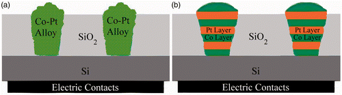
The Si substrates were first exposed by high-energy Ar ions to track them and in order to dig nano-scale wells, the substrates were then etched in HF acid. This process leads to produce holes with a few hundred nanometres deep and a few nanometres width in the SiO2 side of the substrates.
Electrical ohmic contact to each substrate was achieved through a GaIn back contact. It can simply be done by painting the back side of Si substrate by GaIn. An adhesive tape was used to mask-off whole of the substrate except for the area on which deposition was desired. In order to clean the substrate, the Si surface was first put in the following solution successively: (i) acetone with ultrasonic vibration for removing the dust and organic substance and (ii) a mixture solution of H2SO4 and H2O2 for getting rid of the grease and impurities. The Si substrate was then rinsed in deionised water, dried by N2 gas flow and then immediately transferred to the electrodeposition cell. shows a schematic of a porous Si substrate filled with the magnetic (Co) atoms distributed in a non-magnetic (Pt) matrix. Schematic representation of a porous Si substrate filled with Co/Pt multilayer nanowire is shown in .
Figure 1. (Colour online) Schematic diagram of ion etched tracks inside the Si substrate filled by: (a) Co–Pt alloys and (b) multilayer nanowires.
2.2. Nanowire growth
Our nanowires were grown from sulphate electrolyte in a three-electrode cell, containing Co+2 and Pt+4 ions, for growing Co–Pt alloys and Co/Pt nanowire multilayers. The composition of the electrolytes is given as follows:
Cobalt sulphate,CoSO4, 7H2O: 1 mol; | |||||
Hydrogen hexachloro platinic (IV) hexahydrate; H2(PtCl6), 6H2O: 1 mmol; | |||||
Boric acidH3BO3: 0.5 mol. | |||||
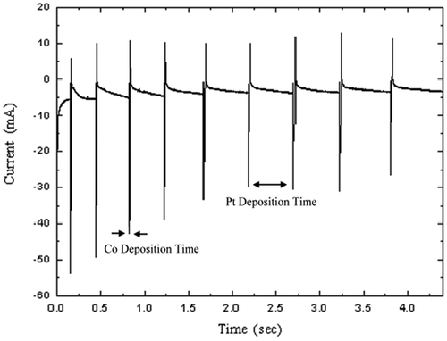
The electrolyte pH was kept constant at 1.5. We used a procedure similar to that described in our previous paper Citation14,Citation15. When a low negative potential is applied to the substrate, only Pt (the more noble of the metals in the electrolyte) will be deposited, while at higher negative potential Co will be deposited to form a ferromagnetic layer. Pt is co-deposited with Co as an impurity in the layer, but Pt concentration in the deposit is kept relatively low by having a low Pt+4 concentration in the electrolyte. Our multilayered nanowire samples were grown by alternating the substrate potential between −0.3 and −3.5 V relative to a saturated calomel reference electrode approximately 2 cm from the substrate. The computer-controlled potentiostat reads the Co and Pt deposition current signals and sends the data to the computer, which is able to plot a graph of the current as a function of time. A current-time profile of an electrodeposited Co/Pt multilayer film is shown in .
Figure 2. Current-time profile for growing of Co/Pt multilayer.
After electrodeposition the samples were removed from electrolyte, washed with distilled water and then dried with N2 gas flow.
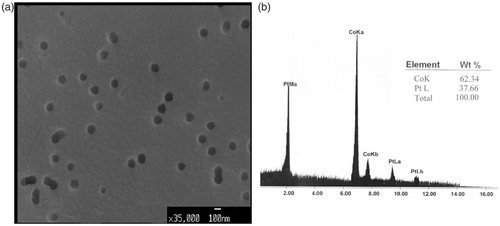
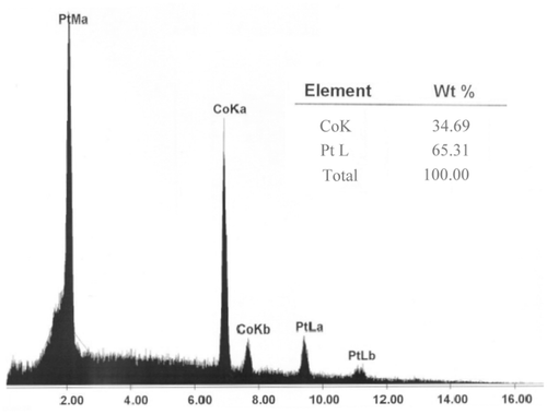
While the holes are filling with Co–Pt/Pt multilayers, the current decreases (its absolute value increases) dramatically. The current then decreases linearly when the holes are filled completely, and some mushroom-shaped islands are formed on the top of each hole. One must be careful and stop the experiment in this stage, otherwise the islands start to grow in three dimensions, join together and make a thin film on the top side of the SiO2 substrate. However, in the case of electric and GMR measurements, having a conductive surface on the both sides of the substrate is an advantage and desirable. An SEM image of a porous Si substrate filled with [Co(5 nm)/Pt(3 nm)] nanowires is shown in . The energy dispersive X-ray microanalysis (EDAX) of the same sample is presented in . The ratio of Co to Pt content in the nanowires is expected to be about 1.67. However, according to , the Co and Pt contents in the Co/Pt multilayer nanowires are estimated to be about 62.34% and 37.66%, respectively. Thus, the ratio of Co to Pt content in the nanowires is about 1.65. In order to make the Co and Pt peaks more obvious, the Si peak is omitted.
Figure 3. (a) SEM image of a substrate surface after filling the pores with Co–Pt nanowires. (b) EDAX spectrum of the sample.
2.3. Magnetic and magnetoresistive measurements
A vibrating sample magnetometer (VSM) was used to study the magnetic properties of electrodeposited superlattices and plot graphs of the magnetic moment as a function of applied magnetic field. Two types of sample holder are available, one in which the sample is mounted horizontally and vibrated vertically so that in-plane moment measurements are made, and one in which the sample is mounted vertically either parallel or perpendicular to the magnetic field and vibrated vertically so that both in-plane and perpendicular measurements can be carried out. All of the VSM measurements were done at room temperature. shows hysteresis loops for Co–Pt alloys and multilayer nanowire samples, respectively. The nominal thickness of Co and Pt layers are chosen to be less than an atomic layer (0.2 nm) so that a Co–Pt alloy is formed instead of forming a well-defined Co/Pt multilayer. The multilayer nanowire sample consists of hundreds of bilayers of [Co(5 nm)/Pt(3 nm)].
Figure 4. Hysteresis loop of: (a) Co–Pt alloy and (b) [Co(5 nm)/Pt(3 nm)] multilayer. Magnetic field is applied parallel to the sample surface.
![Figure 4. Hysteresis loop of: (a) Co–Pt alloy and (b) [Co(5 nm)/Pt(3 nm)] multilayer. Magnetic field is applied parallel to the sample surface.](/cms/asset/95881b7e-8b51-4b69-87c5-2de12a8f4e8f/tjen_a_654273_o_f0004g.gif)
In order to investigate the variation of nanowire resistivity as a function of applied magnetic field and study the magnetoresistance effect, the Co–Pt alloys and multilayer nanowires resistivities were measured as follow: A constant DC current passes through the nanowire (in their length direction) and the potential difference between two sides of the sample was measured. The ratio of voltage to current gives a quantity which is directly proportional to the nanowire resistivity. The Co/Pt sample-filled templates were then located in a magnetic field supplied by a DC electromagnet. Magnetoresistance is defined as a fractional change in the electrical resistance of a material when subjected to a magnetic field Citation16
If the applied field is not large enough to saturate the magnetisation, the resistance at maximum applied field, R Hmax, is used instead of R s. We define nanowire resistance as V/I. The experimental set up for MR measurements is drawn schematically in .
Figure 5. The schematic of experimental set up for MR measurements.
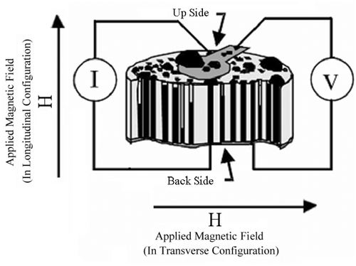
If the applied magnetic field is parallel to the electric current then the obtained MR is known as longitudinal magnetoresistance (LMR), while in the case that the magnetic field is perpendicular to the current, transverse magnetoresistance (TMR) will be obtained.
It was about 160 years ago that William Thomson discovered that the resistivity of nickel and iron changes when they are magnetised. In ferromagnetic materials there is a decrease in the TMR and an increase in the LMR, hence it is known as AMR.
AMR has been observed in thin films as well as in bulk materials. The magnitude of the AMR in thin films depends on the thickness, grain size and film surface conditions and usually a few percent and rarely reaches 5% at room temperature.
In the case that both the TMR and LMR decrease with increasing magnetic field (in contrast to AMR), the phenomena is known as GMR. In most cases the magnitude of the TMR is larger than the longitudinal one, due to an anisotropic component in addition to the GMR. The magnitude of GMR is usually much larger than the AMR value. We define the values of GMR and AMR as follows Citation17,Citation18:
The percentage changes in electric resistance as a function of applied magnetic field (GMR) for a multilayer nanowire consisting of one thousand of bilayers [Co(5 nm)/Pt(3 nm)] in both transverse and longitudinal configurations are shown in , respectively. Since the layering was perpendicular to the long-axis of the wires, it was possible to measure the current-perpendicular-to-plane GMR (CPP-GMR). The magnitude of CPP-GMR we measured is noticeably bigger than the CIP-GMR for the similar systems Citation14.
Figure 6. Transverse (a) and longitudinal (b) magnetoresistance for a [Co(5 nm)/Pt(3 nm)] multilayer nanowire.
![Figure 6. Transverse (a) and longitudinal (b) magnetoresistance for a [Co(5 nm)/Pt(3 nm)] multilayer nanowire.](/cms/asset/0bb83caa-fec8-4c87-87fe-c343854c14cd/tjen_a_654273_o_f0006g.gif)
The magnitude of GMR noticeably depends on the non-magnetic spacer layer and it can be as large at 55% Citation19 at room temperature, the fact that the phenomenon is named as ‘giant’. It has been shown that in certain growth condition, GMR value oscillates as a function of non-magnetic spacer layer Citation20. In most cases, no GMR oscillation with spacer layer thickness could be observed in electrodeposited multilayers in contrast to multilayers produced by physical methods. This may be taken as a strong indication that no alternating antiferromagnetic-ferromagnetic coupling exists in the electrodeposited multilayers. The magnetoresistance curves of electrodeposited multilayer films usually exhibit a splitting around H = 0, especially for thick spacer layers. This is indicative of a weak antiferromagnetic coupling or the absence of a coupling between the magnetisations of neighbouring magnetic layers.
Magnetoresistance measurements for alloy nanowire samples indicate AMR rather than GMR behaviour.
The magnetoresistance curves for a Co–Pt alloy nanowire in both transverse and longitudinal configurations are shown in , respectively. The nominal thickness of both Co and Pt layers has been chosen to be 0.2 nm. As it has been explained in Section 1, a relatively uniform Co–Pt alloy nanowire rather than a multilayer nanowire will be deposited. The Co and Pt contents in the sample are measured using EDX instrument and the result is presented in . The magnitude of AMR for this sample is calculated by subtracting the values of transverse and longitudinal components of MR and as the figures show, the value of 0.71% [0.32–(−0.39)] is obtained. This AMR value is higher than that obtained by Jen et al. for Co–Pt bulk materials Citation21. We found that the MR value in the ‘CPP’ (CPP-MR) configuration – like what is observed in the nanowire systems – is much higher than the value of MR in the ‘CIP’ (CIP-MR) configuration which is usually measured in magnetic/non-magnetic multilayer thin films Citation22,Citation23.
Figure 7. Transverse (a) and longitudinal (b) magnetoresistance for a Co–Pt alloy nanowire.
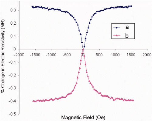
Figure 8. EDAX spectrum for a Co–Pt alloy nanowire.
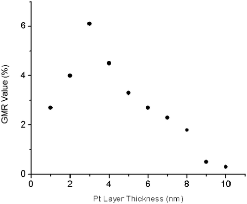
In order to study the effect of the space layer thickness on the GMR value, we grew a series of Co/Pt multilayered nanowires with similar Co thickness of 5 nm but varying the Pt thickness from 1 to 10 nm. The result is presented in . Although the GMR has a maximum value at 6% for a sample with Pt thickness of 3 nm, no oscillatory behaviour was observed in the magnitude of GMR as a function of Pt layer thickness.
Figure 9. GMR as a function of Pt layer thickness for a series of nanowires with similar Co thickness of 5 nm.
3. Summary and conclusion
We successfully electrodeposited Co/Pt multilayer nanowires and alloys into the nano-holes in porous Si templates. Hysteresis loop of the nanowire samples show a very small coercivity and saturation field promising their potential application as the sensitive magnetic sensors in low magnetic field. The maximum CPP-GMR of up to 6% was achieved when the multilayer nanowires are subjected to a magnetic field of 1750 Oe. No oscillatory behaviour was observed in the magnitude of GMR as a function of Pt layer thickness. The Co/Pt alloy nanowires exhibit AMR rather than GMR.
References
- Baibich , M N , Broto , J M , Fert , A , Nguyen Van Dau , F , Petroff , F , Etienne , P , Creuzet , G , Friedrich , A and Chazelas , J . 1988 . Giant magnetoresistance of (001)Fe/(001)Cr magnetic superlattices . Phys. Rev. Lett. , 61 : 2472 – 2475 .
- Bakonyi , I , Tóth , J , Goualou , L , Becsei , T , Tóth-Kádár , E , Schwarzacher , W and Nabiyouni , G . 2002 . Giant magnetoresistance of electrodeposited Ni81Cu19/Cu multilayers . J. Electrochem. Soc. , 149 : 195 – 200 .
- Yamada , A , Houga , T and Ueda , Y . 2002 . Magnetism and magnetoresistance of Co/Cu multilayer films produced by pulse control electrodeposition method . J. Magn. Magn. Mater. , 239 : 272 – 275 .
- Bakonyi , I , Tóth Kádár , E , Cziráki , Á , Tóth , J , Kiss , L F , Ulhaq-Bouillet , C , Pierron-Bohnes , V , Dinia , A , Arnold , B , Wetzig , K , Santiago , P and Yacamán , M J . 2002 . Preparation, structure, magnetic, and magnetotransport properties of electrodeposited Co(Ru)/Ru multilayers . J. Electrochem. Soc. , 149 : C469 – C473 .
- Rizal , C LS , Yamada , A , Hori , Y , Ishida , S , Matsuda , M and Ueda , Y . 2004 . Magnetic properties and magnetoresistance effect in Co/Au, Ag nano-structure films produced by pulse electrodeposition . Phys. Stat. Sol. (c) , 1 : 1756 – 1759 .
- Péter , L , Kupay , Z , Pádár , J , Cziráki , Á , Kerner , Zs and Bakonyi , I . 2004 . Electrodeposition of Co-Cu-Zn/Cu multilayers: Influence of anomalous codeposition on the formation of ternary multilayers . Electrochim. Acta , 49 : 3613 – 3621 .
- Nie , Y , Yang , X , Zhang , P and Sang , H . 2010 . Magnetization and coercivity in Co/Pt multilayers with constant total Co layer thickness . Trans. Nonferrous Met. Soc. China , 20 : 819 – 824 .
- An , Y , Duan , L , Liu , T , Wu , Z and Liu , J . 2011 . Structural and magnetic properties of Pt in Co/Pt multilayers . Appl. Surf. Sci. , 257 : 7427 – 7431 .
- Zhang , F , Wen , F S , Li , L , Wang , N , Lu , Y F , Liu , Z Y , Xu , B , Yu , D L , He , J L and Tian , Y J . 2011 . Investigations on the interlayer coupling in Co/Pt multilayers with perpendicular anisotropy via the extraordinary Hall effect . Thin Solid Films , 519 : 1980 – 1984 .
- Nabiyouni , G and Schwarzacher , W . 1996 . Dependence of GMR on crystal orientation in electrodeposited Co–Ni–Cu/Cu superlattices . J. Magn. Magn. Mater. , 156 : 355 – 356 .
- Alper , M , Attenborough , K , Hart , R , Lane , S J , Lashmore , D S , Younes , C and Schwarzacher , W . 1993 . Giant magnetoresistance in electrodeposited superlattices . Appl. Phys. Lett. , 63 : 2144 – 2146 .
- Nabiyouni , G . Giant magnetoresistance in electrodeposited multilayers, Ph.D. thesis, University of Bristol, UK, 1997
- Nabiyouni , G . 2009 . Design and fabrication of nanomagnetic sensors based on electrodeposited GMR materials . Metrol. Meas. Syst. , 3 : 519 – 229 .
- Nabiyouni , G . 2008 . Giant magnetoresiscance in spintronic Co/Pt nanowire structures . Metrol. Meas. Syst. , 15 : 135 – 143 .
- Naderi , N , Nabiyouni , G and Kazeminezhad , I . 2010 . Growth and electron microscopy study of electrodeposited magnetic Ni nanowires . Int. J. Nanomanuf. , 5 : 163 – 168 .
- Schwarzacher , W and Lashmore , D S . 1996 . Giant magnetoresistance in electrodeposited films . IEEE Trans. Magn. , 32 : 3133 – 3153 .
- O’Handley , R C . 2000 . Modern Magnetic Materials – Principles and Application , New York : Wiley .
- Mc Guire , T R and Potter , R L . 1975 . Anisotropic magnetoresistance in ferromagnetic 3D alloys . IEEE. Trans. Magn. , 11 : 1018 – 1038 .
- Bird , K and Schlesinger , M . 1995 . Giant magnetoresistance in electrodeposited Ni/Cu and Co/Cu multilayers . J. Electrochem. Soc. , 142 ( 4 ) : L65 – L66 .
- Bakonyi , I and Péter , L . 2009 . Electrodeposited multilayer films with giant magnetoresistance (GMR): Progress and problems . Prog. Mater. Sci. , 55 : 107 – 245 .
- Jen , S U , Chen , T P and Chao , B L . 1993 . Saturation moment, specific heat, and transport properties of disordered Co–Pt alloys . Phys. Rev. B , 48 : 789 – 794 .
- Blondel , A , Meier , J , Doudin , B , Ansermet , J-Ph , Attenborough , K , Evans , P , Hart , R , Nabiyouni , G and Schwarzacher , W . 1995 . Wire-shaped magnetic multilayers for ‘current perpendicular to plane’ magnetoresistance measurements . J. Magnet. Magnet. Mater. , 148 : 317 – 318 .
- Fesharaki , MJafari and Nabiyouni , G . A comparison between CPP-GMR in multilayer nanowires and CIP-GMR in multilayer thin films in electrochemically growth Ni-Cu/Cu Systems, J. Mater. Sci. Eng. B 1 (2011), pp. 597–602