
Abstract
Nanocrystalline nickel was produced by pulse reverse microelectroforming. The pulse microelectroforming was also performed for the comparative purposes. The surface morphology and microstructure of electroformed nickel layers were investigated by scanning electron microscopy and X-ray diffractometry. The microhardness of nickel layers was measured with a Vickers microhardness tester. The friction and wear experiments for nickel layers were performed on a friction and wear tester. The results indicate that the nickel layers prepared by pulse reverse microelectroforming exhibit higher density and their grain sizes in the nanometer range. The nickel layers with fine grains, high microhardness and better wear resistance are obtained at positive current density of 20 A/dm2 and negative current density of 2 A/dm2. The microhardness and wear resistance of nickel layers are improved as the positive and negative current densities are increased.
1. Introduction
The development of micro electronic and mechanical system (MEMS) brings to the demand on microcomponents produced with different materials. Microelectroforming has applied to micro-nano-metal structure manufacture, and becomes an important technology of nonsilicon-based fabrication Citation1–4. LIGA is a leading technology for producing high aspect ratio metal microcomponents. A key step during the LIGA process is the electroforming of a metal or metal alloy Citation5,Citation6. The principal advantages of microelectroforming are high-dimensional precision and precise reproduction of surface detail.
Microstructure and mechanical properties are important factors to the quality of electroformed metal microcomponents. The characteristics of polycrystalline metals are intimately related to their grain sizes and relative density, according to fine grain strengthening theory. The influence of grain size on strength or hardness obeys Hall–Petch relationship in the nanometer range; the significant inverse relation was found between hardness and grain size Citation7. Thus, preparation of fine grains and high-density electroformed metal may improve its mechanical properties. Many researchers have found that using pulse current (PC), adding additives and jet electroforming could refine grains of electroformed metals or alloys attained the nanometer range, and improve the mechanical properties Citation8–10. However, additives give rise to difficulties to sustain the composition of electroforming solution. The internal stress of electroformed layers increases; it leads to a surface with cracks or crevices. The shapes of solution spots that are sprayed by a nozzle onto a cathode are difficult to control and compensate in jet electroforming. At present, pulse microelectroforming shows a number of interesting aspects Citation11. It can be used to improve the current distribution and to alter the prevailing mass transport conditions. Pulse microelectroforming can also be used to control the microstructure and composition of electrodeposits Citation12. Electroformed layers of different grain sizes can be achieved, even in the nanometer range if sufficiently high current densities are applied. These nanostructured electroformed metals have recently attracted great attention due to their mechanical response improvement.
In pulse reverse microelectroforming, the current is cathodic pulses followed by anodic pulses, namely pulse reverse current (PRC). PRC has the same effect of replenishing the diffusion layer like PC. PRC reduces the use of additives Citation13 and avoids the drawbacks of additives while the superimposed pulsation keeps control of the crystal structure Citation14,Citation15. Pulse reverse microelectroforming produced ultra-thin and void-free nickel films at 1.2 A/dm2, 90% duty cycle and 400 kHz Citation16. Their excellent precision, durability and surface smoothness make them suitable for high-resolution applications.
In this study, a kind of distinctive current waveform in pulse reverse microelectroforming was put forward to get beneficial morphological and microstructural nanocrystalline nickel. The better mechanical responses of nickel layers are found. The effects of current density on surface morphology, microstructure and average gain size were analysed. Microhardness and wear resistance of nickel layers were studied and these properties were compared with those of nickel layers electroformed with PC.
2. Experimental procedure
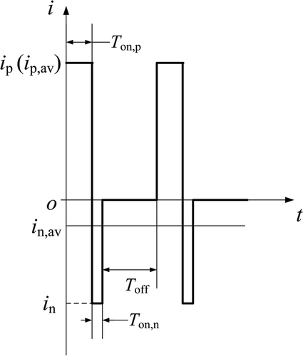
The optimised composition of electroforming solution used in this study was [Ni(NH2SO3)2 · 4H2O] (550 g/L), [NiCl2 · 6H2O] (10 g/L), [H3BO3] (35 g/L) and sodium dodecyl sulphate (SDS, 0.15 g/L) Citation17. The temperature of the solution was 50 ± 0.5°C. The bath pH was adjusted to 3.8–4.5 by adding dilute sulphuric acid. PRC waveform is shown in . The pulse reverse microelectroforming parameters were defined as: positive and negative peak current density (i p, i n), positive and negative average current density (i p,av, i n,av), positive and negative turn-on time (T on,p, T on,n), turn-off time (T off). The values used in the experiment were: the negative average current density was 10% of the positive average current density in pulse reverse microelectroforming; the positive turn-on time (T on,p) and negative turn-on time (T on,n) were 0.3 and 0.1 ms, respectively; the turn-off time (T off) was 0.9 ms; the frequency (f) was 770 Hz; the duty cycle of negative current was 0.1.
Figure 1. Schematic diagram of PRC.
The experimental equipment mainly included a pulse-modulated power and a microelectroforming system. A two-electrode electrolytic cell was applied. The substrate for nickel electroforming was stainless steel (10 × 10 mm2), which was polished followed by weak pickling in 3% H2SO4 solution. The anode was a pure nickel, which helped to maintain the nickel ion concentration in electroforming solution. The nickel layers were rinsed in deionised water and dried immediately after electroforming. The thickness of the electroforming layers was about 30 µm.
The surface morphology of the bath side of the electroformed nickel layers was tested with a scanning electron microscope (SEM JEOL JSM-6360LV) at 20 kV. The microstructures and grain sizes of the electrodeposits were investigated on a transmission electron microscope (TEM PHILIPS EM420). A X-ray diffractometer (XRD SHIMADZU XRD-6000) with a Cu tube was used to characterise the grain sizes and textures of the electrodeposits. The wavelength of Cu-Kα radiation is 0.154056 nm. Each diffraction peak profile was obtained at a slow scan rate of 2°/min. The microhardness was measured using a Vickers microhardness tester (FUTURE-TECH FM-700) with 20 g applied load and a dwell time of 15 s; the results presented in this article are values averaged over more than five indents. The friction and wear properties were performed with a friction and wear tester (CETR UMT-2).
3. Results and discussion
3.1. Microstructure
3.1.1. Influence of negative current on morphology
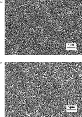
In pulse reverse microelectroforming, as negative current density is changed, other current parameters and process conditions are held constant. While the positive current density is 15 A/dm2, shows the SEM micrographs at 4.5 and 7.5 A/dm2 negative current. The density of nickel layers decreased with increasing negative current density at a constant positive current density. During the negative current, electroformed layers change their potential and become anode, and the overpotential of electroformed layers changes from negative to positive. Under the positive overpotential, the nickel atoms deposited on the surface of electroformed layer turn into nickel ions again, and return back to the electroforming solution. The positive overpotential increases with increasing negative current density. The rate which nickel ions return back to electroforming solution from the surface of electroforming layers increase in a period of pulse reverse microelectroforming. Then the deposition rate of nickel ions on the electroformed layer decreases. The current efficiency of pulse reverse microelectroforming is low. This leads to rougher surface morphology.
Figure 2. Micrographs of nickel layers with different negative current density (SEM) (a) i p,av = 15 A/dm2, i n,av = 4.5 A/dm2 and (b) i p,av = 15 A/dm2, i n,av = 7.5 A/dm2.
3.1.2. Influence of positive turn-on time on morphology
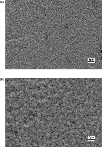
In pulse reverse microelectroforming, as positive turn-on time is changed, other current parameters and process conditions are held constant. While positive current density is 15 A/dm2, the SEM micrographs of nickel layers at 0.5 and 0.7 ms positive turn-on time are shown in . The morphology of nickel layers is influenced by the positive turn-on time. The density of nickel layers decreases with increasing positive turn-on time. The time of deposition to the surface of nickel layers becomes longer and the number of nickel ions turned into atoms increases in pulse reverse microelectroforming, while positive turn-on time is adjusted to last longer. The concentration of nickel ions in the solution near the nickel layer is decreased. This causes concentration polarisation between the nickel layer surface and bulk solution. Thus, the density of the nickel layer decreases.
Figure 3. Micrographs of nickel layers with different positive current turn-on time (a) i p,av = 15 A/dm2, T on,p = 0.5 ms and (b) i p,av = 15 A/dm2, T on,p = 0.7 ms.
3.1.3. Grain size and distribution
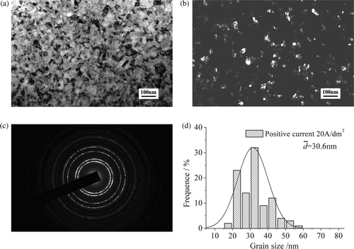
Nickel layers were prepared with varying positive and negative current density in pulse reverse microelectroforming. The TEM micrographs of nickel layers are shown in . are bright-field and dark-field images of nickel layers at positive current density of 20 A/dm2 and negative current density of 2 A/dm2, respectively. shows the electron diffraction image. The four rings express (111), (200), (220) and (311) textures of nanocrystalline nickel layer from inside to outside. As seen in , the direction distribution of grains in the nickel layer is enhanced for continuous diffraction rings. The grain sizes of nickel layers attain the nanometer range.
Figure 4. TEM micrographs of nickel layers with PRC (i p,av = 20 A/dm2, i n,av = 2 A/dm2) (a) bright-field image, (b) dark-field image, (c) electron diffraction image and (d) grain size distribution.
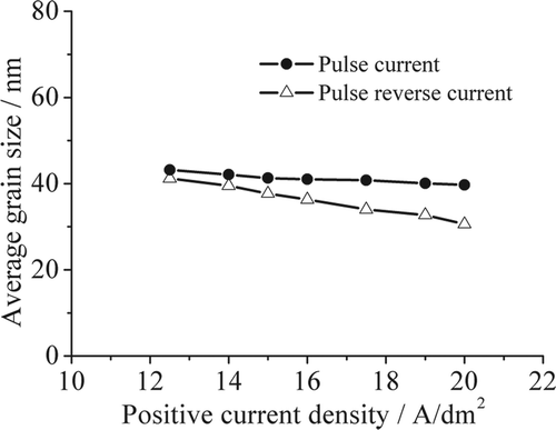
shows the variation of gain size with current density for pulse reverse microelectroforming. The grain sizes of nickel layers decrease with increasing current density. The grain sizes of nickel layers prepared by pulse reverse microelectroforming are smaller than those of nickel layers prepared by pulse microelectroforming, and the PRC decreases the grain sizes faster than the PC does at equal positive current density. The average grain size of the nickel layer decreases to 30.6 nm at the positive current density of 20 A/dm2 and negative current density of 2 A/dm2, under PRC conditions.
Figure 5. Average grain size as a function of current density.
In pulse reverse microelectroforming, the electric double layer discharges once positive current is turned off. Meanwhile the negative current density is turned on. The discharge time that the positive current decays from initial value to zero is rapidly shortened Citation18. The grain growth on the deposit surface is impeded effectively during the discharge time. The effect of negative current on decreasing grain size is more significant with increasing current density. The electroformed layer becomes anode during the negative current turn-on time. The dissolution of the layer occurs. Some nickel atoms extruding from the surface of the electroformed layer are redissolved; the nickel atoms on the grains, which adsorption is low, may also be dissolved back to the bulk solution. As a result, the crystal grains of the electroformed layer are refined.
Peak profiles of XRD pattern could broaden while the grain size of electroformed layer decreases. They manifestly widen once grain size decreases to the magnitude of nanometers Citation19. The average grain size d is evaluated from the full-width at half-maximum (FWHM) β according to Scherrer formula as follows
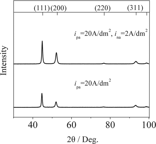
X-ray diffraction patterns () were obtained for the electroformed layers prepared by pulse reverse and pulse microelectroforming at the positive current density of 20 A/dm2. The preferred orientation is in the (111) and (200) double fibre texture. To pulse reverse electroformed layer, the intensity values of (111) and (200) peaks are enhanced compared to the pulse electroformed layer at an equal positive current density. The FWHM of the pulse reverse electroformed layer is broader than that of pulse electroformed layer. The average grain size of pulse reverse electroformed layer is smaller than that of pulse electroformed layer according to Scherrer formula. The result is consistent with TEM dark-field measurement.
Figure 6. XRD patterns of electroformed layers with PRC and PC.
3.2. Mechanical properties
3.2.1. Microhardness
The nickel layers were obtained by pulse reverse microelectroforming under different positive and negative average current density conditions. The negative average current density remains 10% of the positive average current density. While positive and negative current densities are changed, T on,p, T on,n and T off are held constant. The microhardness of the pulse deposits was also measured in order to compare them with that of the pulse reverse deposits. shows the microhardness as a function of current density in pulse reverse and pulse microelectroforming, respectively. Microhardness noticeably increases with increasing positive and negative current densities in pulse reverse microelectroforming. The microhardness of the pulse reverse deposits is higher than that of the pulse deposits at the equal positive current density. The microhardness value of the pulse reverse deposits is equal to 564 HV at a positive current density of 20 A/dm2 and a negative current density of 2 A/dm2.
Figure 7. Microhardness as a function of current density.
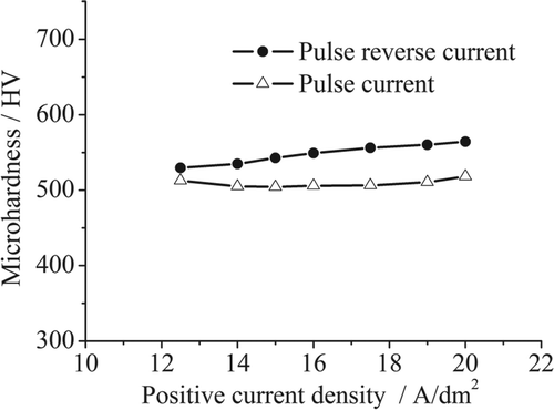
The negative current impedes the grain growth on the deposition surface during the decay of positive current in pulse reverse microelectroforming. The average grain size of pulse reverse deposits becomes smaller than that of pulse deposits electroformed at an equal positive current. The improved microhardness of the pulse reverse deposits is due to their finer nanostructures. According to the strengthening mechanism, the increase in microhardness can be attributed to the increased density of grain boundary in refined nanocrystalline nickel, which helps to block the dislocation motion, thus enhancing the resistance to plastic deformation.
3.2.2. Friction and wear property
The wear resistance experiment of electroformed layer was conducted on the friction and wear tester. A GCr15 steel ball with radius of about 2.5 mm was used. The ball-on-disc wear experiment was performed on the surface of electroformed layer, with the friction parameters being a fixed load of 0.4 N, sliding velocity of 0.7 m/s and reciprocating motion distance of 5 mm. The experiment was conducted at a room temperature without lubrication. The sliding time was 30 min.
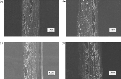
shows the SEM micrographs of the worn morphology of electroformed layers. depicts the pulse reverse deposits, and depicts the pulse deposits. The worn widths of the pulse reverse and pulse deposits increase with increasing positive PC density; the wear resistance is decreased. The wear resistance of pulse reverse deposits is better than that of pulse deposits electroformed at an equal positive current density.
Figure 8. Worn morphology of nickel layers with PRC and PC (SEM) (a) ip,av = 15 A/dm2, in,av = 1.5 A/dm2, (b) ip,av = 20 A/dm2, in,av = 2 A/dm2, (c) ip,av = 15 A/dm2 and (d) ip,av = 20 A/dm2.
The overpotential is increased with increasing current density. The adhesion among grains is lower because the electroforming speed is faster. This decreases the wear resistance of both pulse reverse deposits and pulse deposits. In addition, the grain sizes of pulse reverse deposits decrease faster than those of pulse deposits while the positive current density increases; the microhardness of pulse reverse deposits is increased. The fine grain sizes and higher microhardness of nickel layers could improve their friction and wear property. On the other hand, the dissolving process happens on the surface of electroformed layers during negative current in pulse reverse microelectroforming. The lower adhesion grains are dissolved back to the solution. Meanwhile, the adhesion of new grains electroformed on the surface of nickel layer is enhanced because of a surface activation effect during the negative current turn-on time. Thus, the wear resistance of pulse reverse deposits is prior to that of pulse deposits electroformed at an equal positive current.
The plastic deformation happens on the surface of electroformed layer in the friction process. There are some parallel wear scratches in friction channels formed by micro cutting. The abrasive dusts exert while the steel ball moves against the surface of electroformed layer. The parallel wear scratches appear once abrasive dusts entry the friction channels.
The wear volume loss of electroformed layer yields Citation20
The rate of wear volume loss is
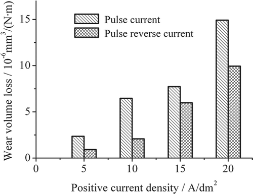
shows the rates of wear volume loss of pulse reverse and pulse microelectroforming. The rate of wear volume losses increase with increasing positive current density. The rate of wear volume loss of pulse reverse deposits is lower than that of pulse deposits electroformed at an equal positive current.
Figure 9. Rates of wear volume loss of electroformed layers.
4. Conclusions
In pulse reverse microelectroforming, the discharge time of double electric layer between deposit surface and solution is shortened. So, the grain growth is suppressed during the decay of positive current time. The electroformed layer becomes an anode during negative turn-on time. Some nickel atoms with low adsorption may be dissolved back to the bulk solution. As a result, nanocrystalline nickel is got.
The electroformed nickel with small grains and high density could be prepared by pulse reverse microelectroforming. The microhardness and the wear resistance of pulse reverse deposits are better in comparison with those of pulse deposits. This kind of pulse reverse microelectroforming could improve the quality of electroformed microstructure.
This study raises the possibility of tailoring nanocrystalline nickel with good mechanical properties for metal microcomponents by selecting the appropriate pulse reverse micro-electroforming conditions.
Acknowledgements
The authors would like to thank for the support of the National Natural Science Foundation of P.R. of China (No. 51075057, No.50675025 and No. 51105060).
References
- Tsai , M C and Hsu , L Y . 2007 . Winding design and fabrication of a miniature axial-flux motor by micro-electroforming . Mag. IEEE Trans. , 43 : 3223 – 3228 .
- Ertan , A , Tewari , S N and Talu , O . 2008 . Electrodeposition of nickel nanowires and nanotubes using various templates . J. Exp. Nanosci. , 3 : 287 – 295 .
- Ma , R , Sask , K N , Shi , C , Brash , J L and Zhitomirsky , I . 2011 . Electrodeposition of polypyrrole-heparin and polypyrrole-hydroxyapatite films . Mater. Lett. , 65 : 681 – 684 .
- Bouwhuis , B A , McCrea , J L , Palumbo , G and Hibbard , G D . 2009 . Mechanical properties of hybrid nanocrystalline metal foams . Acta Mater. , 57 : 4046 – 4053 .
- Morales , A M , Domeier , L A and Gonzalesa , M . 2003 . Microstructure and mechanical properties of nickel microparts electroformed in replicated LIGA molds . Proc. SPIE , 4797 : 440 – 447 .
- McGeough , J A , Leu , M C , Rajurka , K P , De Silva , A KM and Liu , Q . 2001 . Electroforming process and application to micro/macro manufacturing . CIRP Ann. ManTech. , 50 : 499 – 514 .
- Ibanez , A and Fatas , E . 2005 . Mechanical and structural properties of electrodeposited copper and their relation with the electrodeposition parameters . Surf. Coat. Tech. , 191 : 7 – 16 .
- Meyers , M A , Mishra , A and Benson , D J . 2006 . Mechanical properties of nanocrystalline materials . Prog. Mater. Sci. , 51 : 427 – 556 .
- Lim , J H , Park , E C , Joo , J and Jung , S B . 2009 . Effect of additives on microstructure and mechanical properties of nickel plate/mask fabricated by electroforming process . J. Electrochem. Soc. , 156 : 108 – 112 .
- Tian , Z J , Wang , D S and Wang , G F . 2010 . Microstructure and properties of nanocrystalline nickel coatings prepared by pulse jet electrodeposition . Trans. Nonferrous Met. Soc. China , 20 : 1037 – 1042 .
- Rybakova , N , Souto , M and Andriyko , Y . 2009 . Morphology and mechanical properties of TiB2 coatings deposited from chloride-fluoride melts by pulse electroplating . J. Electrochem. Soc. , 156 : 131 – 137 .
- Landolt , D and Marlot , A . 2003 . Microstructure and composition of pulse-plated metals and alloys . Surf. Coat. Tech. , 169–170 : 8 – 13 .
- Awad , Y , Lavallee , E , Beauvais , J , Drouin , D , Mun , L K , Yang , P , Cloutier , M and Turcotte , D . 2007 . Nickel pulse reversal plating for image reversal of ultrathin electron beam resist . Thin Solid Films , 515 : 3040 – 3045 .
- Yin , K M . 2003 . Mathematical model of galvanostatic pulse with reverse plating in the presence of a surface blocking agent . J. Electochem. Soc. , 150 : C435 – C439 .
- Leisner , P , Fredenberg , M and Belov , I . 2010 . Pulse and pulse reverse plating of copper from acid sulphate solutions . Trans. Inst. Met. Finish. , 88 : 243 – 247 .
- Tang , P T . 2007 . Pulse reversal plating of nickel alloys . Trans. Inst. Met. Finish. , 85 : 51 – 56 .
- Du , L Q , Jia , S F , Nie , W R and Wang , Q J . 2011 . Fabrication of fuze microelectromechanical system safety device . Chin. J. Mech. Eng. , 24 : 836 – 841 .
- Shao , L G , Du , L Q and Wang , L D . 2010 . Development of nanocrystalline nickel by pulse reverse microelectroforming . Micro Nano Lett. , 5 : 165 – 170 .
- Jensen , H , Pedersen , J H , Jørgensen , J E , Skov Pedersen , J , Joensen , K D , Iversen , S B and Søgaard , E G . 2006 . Determination of size distributions in nanosized powders by TEM, XRD, and SAXS . J. Exp. Nanosci. , 1 : 355 – 373 .
- Li , J , Wu , Y Y , Wang , D L and Hu , X G . 2000 . The microstructure and wear resistance characteristics of electroformed nickel and partially stabilized zirconia composite coatings . J. Mater. Sci. , 35 : 1751 – 1758 .