Abstract
In this article, we report our recent results on the synthesis of nano-ink and drop-casted films of CuInGaS2 (CIGS), which acts as the absorber material for CIGS-based solar cells. The morphological and optical property changes of CIGS films have been compared to those of nano-CuInS2 (CIS) films deposited on glass substrates. It is found that the microstructure and morphology of these films depend strongly on the presence of Ga. High-resolution transmission electron microscopy reveals that CIGS nanoparticles are 4–5 times larger than CIS nanoparticles. The roughness of CIGS films could be reduced on preheating the drop-casted films prior to sulphurisation. The absorption onset for CIGS is lower than that of CIS due to Ga substitution in place of In. Raman spectra showed a noticeable contribution from Cu–Au mode in CIGS films. Larger nanoparticles in CIGS are attributed to faster growth kinetics due to higher Cu:In ratio than in CIS.
Keywords:
1. Introduction
It is now clear in the scientific society that silicon-based photovoltaic materials are expensive with poor optical properties, and its coverage of the solar spectrum is limited. Hence, the dominance of bulk silicon solar cells in the market is changing, though slowly. Polysilicon prices are ever rising, and this is leading to serious supply constraints. These short falls in silicon technology have led to the growth of considerable interest in thin-film solar cells. In bulk silicon cells, module area is tiled with silicon wafers, whereas in thin-film cells, large substrates are coated as single units. The cost per square metre of cell area is low, and thin-film cells can be fabricated on flexible substrates giving us more options of cell installation. Growth and fabrication of CuInS2 (CIS) and CuInGaS2 (CIGS) is one such thin-film technology. These compounds include a mixture of quaternary and ternary alloys, with indium and gallium substituting for each other, and sulphur is sometimes used instead of or in addition to selenium. The electrical properties of CIGS materials depend on the exact composition with band gap ranging from 1.0 to 3.5 eV. With this flexible band gap, CIGS compounds provide us a different spectrum from that of normal sunlight and can cover a wider fraction of the optical spectrum. There are many low-cost techniques such as spray pyrolysis, paste coating, doctor blade method and spin coating to deposit thin films of CIS. This is one of the most important factors, which plays a key role in deciding the industrial applications of photovoltaic materials. A compact thin film with smooth surface is essential for the fabrication of high-efficiency cells. These materials attract attention due to their size and shape-dependent properties also Citation1–3. During the preparation stages, CIGS is vulnerable to easy oxidation process, and hence, the preparation of nano-CIGS is a big challenge as the starting components when driven to the nano-form change their physical properties. In this work, we have synthesised CIS and CIGS nano-inks followed by thin-film fabrication using a simple and feasible non-vacuum approach for the preparation of a dense CIS thin film with smooth surface and observed changes in morphology with Ga addition. The structure, microstructure and morphology of as-grown films are determined using X-ray diffraction (XRD), scanning electron microscopy (SEM) and energy dispersive X-ray spectroscopy (EDS).
2. Synthesis of nano-ink and films
The nanocrystals of CuIn0.8Ga0.2S2 and CuInS2 were synthesised using stoichiometric weights of chlorides of respective elements. A solution of these chlorides in oleylamine was prepared and heated at 130°C in a three-necked flask while being continuously purged with Ar to prevent any oxidation. A solution of sulphur in oleylamine is injected into this hot solution and heated at 230°C for 30 min. After cooling the mixture down to 60°C, the particles are dispersed in toluene, followed by ethanol to flocculate the particles. The nanoparticles are centrifuged for 20 min at 10,000 rpm and the precipitate is collected. This precipitate is re-dispersed in toluene to form a nano-ink solution. The nano-ink of CIGS and CIS is first drop-casted and then slit-casted on glass substrates. These films are then preheated at 220°CC followed by sulphurisation at 500°C for 1 h in a tubular furnace in the presence of high-pure N2. Resulting absorber layers were black in colour similar to that of nano-ink.
3. Results and discussion
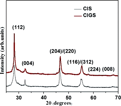
The crystal structure of these films was determined by XRD using Cu-Kα radiation of 1.5418 Å. shows XRD patterns of CIS and CIGS layers. An intense peak at 2θ = 27.9° oriented along (112) direction and other prominent peaks observed at 46.5° and 55.0° indicate the chalcopyrite structure of CIS. The peak pattern is in good agreement with the Joint Committee on Powder Diffraction Standards reference diagrams for the corresponding bulk phases.
Figure 1. XRD patterns of CIS and CIGS films grown at 500°C corresponding to the chalcopyrite structure of CIS.
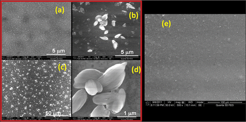
Surface morphology of the absorber layers of CIS using high-resolution SEM (HRSEM) images reveals a uniform coating of CIS nano-ink on glass (). However, the CIGS layer consisted of a thin film along with several petal-like structures forming clusters at various places all over the film (). These structures are elongated in shape and definitely greater in size than the CIS particles constituting the CIS films. So, the film surface morphology seems to be rough for CIGS films. This morphology is an obstacle to make a flawless junction of the CuInGaS2 film with buffer layer. The preparation of the CuInGaS2 film with smoother morphology is essential for the fabrication of high-efficiency cells Citation4. Therefore, further optimisation of growth parameter was carried out to improve the surface quality of the CuInGaS2 layers grown by the sulphurisation technique. The drop-cast films were preheated in ambient air at different temperatures before final sulphurisation temperature of 500°C. This additional factor seemed to change the morphology for good and it was found that the films preheated at 220°C had a comparatively lower roughness than the films that were not preheated before sulphurisation (). It can be seen that the roughness of the film improves. Further studies for optimisation such as thickness variation and annealing time are being carried out to further decrease the roughness.
Figure 2. HRSEM images of (a) CIS and (b)–(d) CIGS nanostructured film and (e) HRSEM image of 220°C preheated CIGS film.
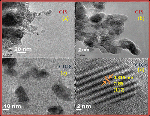
To know the exact particle size, high-resolution transmission electron microscope (HRTEM) images of the nanoparticles forming the film were recorded. A small portion of the film was collected and ultrasonicated in acetone for HRTEM sample preparation. One or two drops of this solution were dropped on carbon-coated grids and dried overnight for analysis by HRTEM. reveals a narrow size distribution of 4–5 nm for CIS nanoparticles, whereas shows a comparatively broader distribution (10–20 nm) of particle size for CIGS nanostructured film. The shape of the investigated nano grains is mostly spherical in CIS films, whereas CIGS films display elongated particles.
Figure 3. HRTEM images of (a)–(b) CIS, and (c)–(d) CIGS nanoparticles.
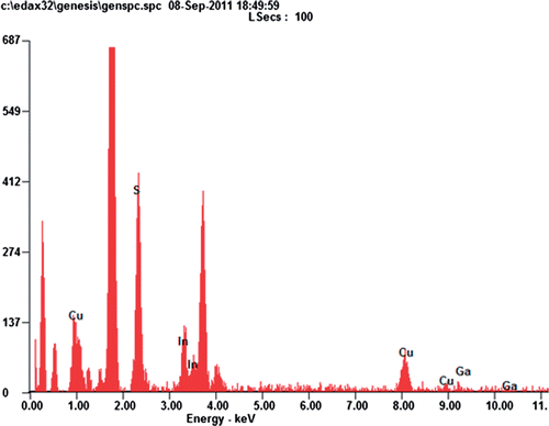
Quantisation from the EDS spectra of CIS films shows that the Cu:In ratio ∼1:1. This leads to a slower reaction Citation5 as well as growth rate leading to the formation of uniform nanoparticles of diameter ∼5 nm. For CIGS films, because Ga replaces In, Cu:In ratio > 1:1 (). This composition ratio leads to a comparatively faster reaction rate resulting in the growth of some larger particles, which appear as clusters all over the film. Preheating leads to nucleation on the substrate surface even before sulphurisation. This buffer growth helps us to grow smoother films.
Figure 4. EDS spectra of CIGS film.
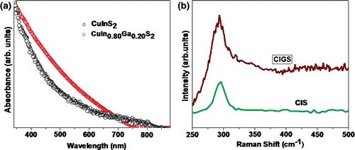
Absorbance study () was carried out to determine the onset of absorption. For CIS films, the absorption edge is ∼790 nm, and for CIGS, it is ∼750 nm. This gives an approximate band gap of 1.57 and 1.65 eV for CIS and CIGS, respectively. This value is larger than the bulk value of 1.5 eV. For CIS, the enhanced value can be accounted for by the presence of quantised nanocrystals with diameter ∼5 nm, which is less than the exciton radius Citation6 of 8 nm. The shift in the absorption spectra of CIGS film is a simple pointer of Ga substitution in the CIS matrix. shows the Raman spectra of these films with a broad peak around 295 cm−1. On de-convoluting this peak, we could find a small contribution (305 cm−1) from Cu–Au polymorph in the case of CIGS films. This polymorph is obtained by permuting all Cu atoms with Indium atoms in every two consecutive planes leaving the next two consecutive planes unpermuted and corresponds to the defect phase (anti-phase defect).
Figure 5. (a) Absorption spectra of CIS and CIGS films grown at 500°C and (b) Raman spectra of CIS and CIGS nanostructured films grown at 500°C.
4. Conclusion
We have prepared CuInGaS2 nano-ink by injection method and fabricated corresponding thin films by drop-casting followed by sulphurisation. The surface morphology of the CIGS films can be improved by preheating the films before sulphurisation. A compact CIGS film with relatively smoother surface could be obtained with a preheating temperature of 220°C. The roughness of CIGS films could be reduced on preheating the drop/slit-casted films prior to sulphurisation. The absorption onset for CIGS is lower than that of CIS due to Ga substitution in place of In. Raman spectra show a noticeable contribution from the Cu–Au mode in CIGS films. There is a definite change in morphology of CIS films with Ga addition. Larger size of nanoparticles in CIGS is attributed to faster growth kinetics due to higher Cu:In ratio than that in CIS films.
Acknowledgements
We would like to acknowledge BHEL, R & D, Hyderabad for providing the financial support for this work under the grant RD/1112/PHY/001/BHEL/MSRA and Department of Science and Technology for helping us set up Nanofunctional Materials and Technology Centre with various experimental facilities used in this work.
References
- Alivisatos , A P . 1996 . Perspectives on the physical chemistry of semiconductor nanocrystals . J. Phys. Chem. , 100 : 13226 – 13239 . doi: 10.1021/jp9535506
- Murray , C B , Kagan , C R and Bawendi , M G . 2000 . Synthesis and characterization of monodisperse nanocrystals and close-packed nanocrystal assemblies . Annu. Rev. Mater. Sci. , 30 : 545 – 610 . doi: 10.1146/annurev.matsci.30.1.545
- Xie , R , Rutherford , M and Peng , X . 2009 . Formation of high-quality I-III-VI semiconductor nanocrystals by tuning relative reactivity of cationic precursors . J. Am. Chem. Soc. , 131 : 5691 – 5697 . doi: 10.1021/ja9005767
- Nakamura , S and Yamamoto , A . 1997 . Preparation of CuInS2 films with sufficient sulfur content and excellent morphology by one-step electrodeposition . Sol. Energy Mater. Sol. Cells , 49 : 415 – 421 . doi: 10.1016/S0927-0248(97)00122-0
- Czekelius , C , Hilgendorff , M , Spanhel , L , Bedja , I , Lench , M , Muller , G , Bloeck , U , Su , D and Giersig , M . 1999 . A simple colloidal route to nanocrystalline ZnO/CuInS2 bilayers . Adv. Mater. , 11 : 643 – 646 . doi: 10.1002/(SICI)1521-4095(199906)11:8<643::AID-ADMA643>3.0.CO;2-I
- Marta , K , Holger , B , Jurgen , P and Joanna , K-O . 2010 . A simple colloidal route to nanocrystalline ZnO/CuInS2 bilayers . J. Am. Chem. Soc. , 132 : 15976 – 15986 . doi: 10.1021/ja103828f