
Abstract
We performed impedance spectroscopy studies on intercalated multilayer structures of type-layered inorganic semiconductor (gallium selenide and indium selenide)/organic semiconductors (N,N′-dimethyl-3,4,9,10-perylenetetracarboxylic diimide), which revealed the appearance of low-frequency inductive response as a result of intercalation of organic semiconductors (OS) into inorganic semiconducting layers. A current–voltage characteristic has the shape of Coulomb steps with a step 0.32 V that are blurred due to superimposition of electric field and illumination. An applied electric field and illumination during the introduction of OS leads to the formation of electrets and photoelectret states that modify polarisation and photoprocesses in accordance with the conductivity type of nonorganic matrix.
1. Introduction
Formation of heterostructured nonorganic/nonorganic, nonorganic/organic and bio/nonorganic nanocomposite materials recently attracts increased attention from the point of view of obtaining the structures having a wide spectrum of novel properties Citation1,Citation2. However, the well-known techniques of preparation of these structures such as vacuum deposition, photolithography, and Langmuir–Blodgett technique have certain disadvantages due to a limited choice of different heteroingredients as well as due to problems arising in the synthesis of a ‘host-guest’ architecture. However, in the latter systems, it is possible to attain not only a controlled change of the initial atomic-molecular structure and force fields of the host-materials as well as synthesis of chemical substances in their intracrystalline field, but also to form certain structures at atomic-molecular level and complex functional blocks. This can be done using intercalation, i.e. by introducing guest components into crystal-structured regions affected by van der Waals forces of host-materials. The intercalation technologies are capable for formation of certain complicated atomic-molecular complexes by using a certain sequence of chemical reactions and at the same time providing a reliable anticoagulation matrix isolation of nanosystems Citation3.
Currently, this technology is under development with some progress achieved recently Citation4–6. In Citation7, intercalated multilayer structures of the type of a layered inorganic semiconductor indium selenide (InSe)/conducting polymer poly(3,4-ethylenedioxythiophene) : poly(styrenesulfonate) (PEDOT : PSS) were studied, PEDOT : PSS – organic conductor with high conductivity serves as a guest organic component. This article proposed a principally new technological approach – namely, the imposition of external physical fields and their coupling in the formation of inorganic/organic nanohybrids based on organic photosensitive semiconductor DiMe-PTCDI and layered semiconductors of gallium selenide (GaSe) and InSe.
2. Conceptual postulates and experimental techniques
The layered semiconductors of GaSe and InSe were chosen as basic objects (host-materials) in our experiments. The GaSe and InSe single crystals grown by the Bridgman–Stockbarger technique had a clearly defined layered structure with p- and n-type of conductivity, respectively. The band gap width (according to optical data) is 2.02 eV for GaSe and 1.22 eV for InSe single crystals. It is well known Citation8,Citation9 that they are characterised by the availability of the so-called guest positions oriented perpendicular to the crystallographic axis-c of the regions with weak action of van der Waals forces. The introduction of extraneous ions, atoms or molecules into definite intracrystalline spaces is known as intercalation phenomenon Citation10. The peculiarities of crystalline structure of these materials do not require a precise mechanical and chemical treatment of the surface and cause an increased inertness to the adsorption of foreign atoms or molecules. The absence of broken bonds upon their surfaces ensures a very low speed of surface recombination. Furthermore, they are characterised by high photosensitivity within the visible spectral region.
On the other hand, organic semiconductors (OS), which possess interesting physical properties, become widely used for different applications Citation11. Thus, a multilayered configuration of such nanostructure is capable for revelation of new phenomena as well as their applications.
Since the molecules of the N,N′-dimethyl-3,4,9,10-perylenetetracarboxylic diimide (DiMe-PTCDI) Citation12 are not directly introduced into GaSe or InSe, the following three-step scheme of crystal engineering () was utilised in order to form the intercalate nanostructures. At first, the natrium nitrite is introduced into the initial matrix by a direct exposition of semiconductor monocrystal melt at 300°C for 5–10 min. As a result of n-step ordering Citation13,Citation14, the distance between the corresponding layers significantly increases ().
Figure 1. The stages of formation of hybrid multilayered GaSe<DiMe-PTCDI> and InSe<DiMe-PTCDI> structures. The inset represents the chemical structure of DiMe-PTCDI.
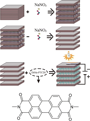
The next step was the deintercalation of natrium nitrite from the crystal by its extraction during five 24-h periods and subsequent drying at temperature of 110°C and at lowered pressure. Deintercalated matrices became suitable for introducing the OS due to the weakened van der Waals bonds and the modified intracrystalline force fields. The third step consisted in the intercalation of OS into an expanded crystal lattice via direct deeping of the obtained deintercalated matrix in solution of DiMe-PTCDI in acetone at room temperature for 48 h. Then one group of samples with introduced DiMe-PTCDI were dried at room temperature (the so-called normal conditions), while the second and third group were dried at room temperature too, but with an electric field (voltage 1.5 V) applying along the crystallographic axis-c and with or without simultaneous illumination by visible light, respectively.
The X-ray diffraction (XRD) data were collected by a computer-controlled DRON-3 powder diffractometer using filtered Co-Kα radiation. Qualitative analysis was carried out with a mass spectral analyser IEU-100 (Balzers).
The impedance measurements in the direction of crystallographic axis-c have been carried out within the frequency range 10−2–105 Hz using the measurement complex ‘AUTOLAB’ (ECO CHEMIE) completed with FRA-2 and GRES software. Frequency dependencies of the complex impedance Z were analysed using a graphoanalytical method in the packaged software environment ZView2.3 (Scribner Associates). Approximation errors did not exceed 4%. All the expanded samples prior to the introduction of DiMe-PTCDI had a linear current–voltage characteristic in the voltage range from −3 V to +3 V.
3. Results and discussion
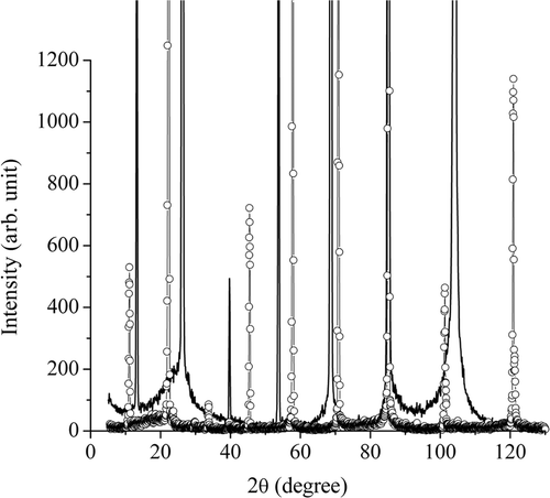
The results of XRD investigations of GaSe single crystals before and after introduction of DiMe-PTCDI samples are shown in . First of all, it should be noted that after the intercalation, the reflexes intensity decreased (in about four times at 2θ = 25.9°) except the angular of 2θ = 55°, where it has doubled upon intercalation. Second, one has to account that after intercalation of DiMe-PTCDI, the number of intense reflections increases in the range of diffraction angles of 2θ = 5°–120°. Herewith, the low angular reflexes (2θ = 11.1° and 22°) shifted to small angle region in comparison to the original matrix reflections (2θ = 13.3° and 25.9°, respectively), and high angular reflexes (2θ = 70.8° and 85°) shifted to high angle region. Thus, it is observed not only increasing of the identity parameter along the crystallographic axis-c, but also the appearance of additional diffraction maxima that indicate a dramatical change of the structure due to intercalation of GaSe by DiMe-PTCDI. Comparison of additional spectrum with standards radiographs datebase JCPDS (Issue 1–22) are not allowed to include additional lines or systems to one of the phases Ga–Se–Fe–COH, contained in the database. However, data qualitative analysis revealed the presence of C, N and O elements (unfortunately, this technique is not capable for hydrogen identification) in intercalated samples. Due to the double expansion of GaSe samples after the introduction of DiMe-PTCDI, the position of additional spectrum diffraction maxima, and well-known fact that the formation of intercalated molecular ‘guests’ is the mechanism of N-barrier structure Citation7,Citation10,Citation13–15. Estimation shows that the fabricated nanohybrid structure should be attributed to the periodic configuration of the third stage. It means that van der Waals regions where the DiMe-PTCDI molecules are localised have expanded approximately seven times. Moreover, it should be noted that introduction of DiMe-PTCDI in every third interlayer space leads to increase of the interlayer distance in regions without the organic guest. The data of gravimetric measurements showed that the volume of embedded DiMe-PTCDI (in terms of density of DiMe-PTCDI) is 37 ± 3 vol.% with respect to the initial GaSe.
Figure 2. X-ray diffraction pattern of GaSe before (solid line) and after (circle) introduction of DiMe-PTCDI.
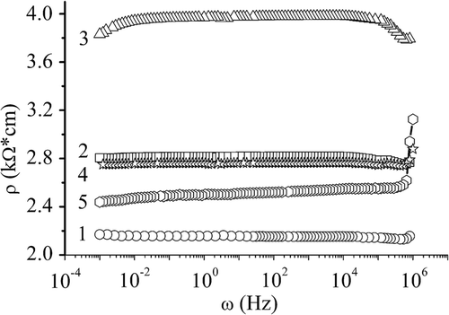
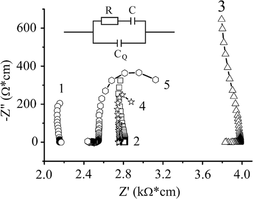
presents frequency dependencies of the real component of specific impedance measured perpendicular to the planes of layers (ρ(ω)). One can see that the formation of molecular interlayers of the OS in an expanded matrix GaSe leads to a 10-fold increase of ρ(ω). Most probably, it is caused by the localisation of carries in quantum wells formed by semiconductor nonorganic nanointerlayers as well as by the decline of mobility due to barriers formed by the OS. Formation of OS within the expanded crystal matrix under an applied permanent electric field of 11.5 V cm−1 leads to saturation ρ(ω) (curve 3, ). On the other hand, simultaneous illumination of the sample by light during the formation of OS in the electric field similarly to measurements in the light wave field (curve 4, ) practically diminish ρ(ω) change. Furthermore, an essential narrowing of the frequency interval of downfalling high-frequency branches at the superimposition of electric field and illumination testifies the growth of contribution of delocalised carries to the electrical conduction at the background of the carriers skipping the localised states Citation16. An evidence for such a mechanism is clearly seen in (curve 2), where there is a frequency interval of the dependence ρ(ω) ∼ at frequencies above 100 Hz, which actually proves the skipping conductance according to Geballe–Pollak theory Citation17. The abovementioned can also be confirmed by the Nyquist diagrams () plotted as a dependence of the imaginary part of complex impedance on its real part. Their arc-wise character in the first quadrant, whose general replacement scheme (equivalent circuit) represents a parallel connection of resistor and capacitor, indeed indicates a complete capacitive response of localised states, and consequently confirms the hopping conductance or delocalisation of carriers into the tails of state density or into the regions of delocalised state. Herein, a distinct visualisation of frequency dispersion of low-frequency branch (a two-arc character of the curve 2 in the 1st quadrant) represent an essential contribution of the additional barrier formed by two semiconductor phases of different conductivity type into the kinetics of current flow. In this case, if the charge carriers will be held in quantum wells during the period equal to half-period of sine signal, we should expect the appearance of inductive response which is referred to as the phenomenon of negative capacitance. This phenomenon is known in the literature, though its mechanism has not been yet unambiguously explained Citation18,Citation19. Generally, an inductive behaviour is observed even in the case when the charge is introduced into the layers of small and subsmall sizes that are in the range of a few nanometers Citation20.
Figure 3. Frequency dependences of a real component of specific impedance perpendicular to the layers of expanded matrix GaSe prior to – (1) and after the formation of molecular interlayers of the OS at normal conditions – (2) and at superimposition of electric field – (3), (4) – curve 3, measured at illumination.
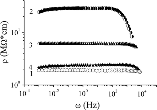
Figure 4. Nyquist diagrams constructed for an expanded matrix GaSe along crystallographic axis C prior to – (1) and after the formation of molecular interlayers of OS at normal conditions – (2), as well as at the action of electric field – (3).
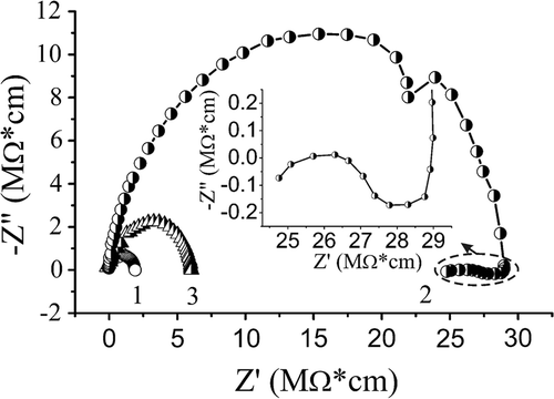
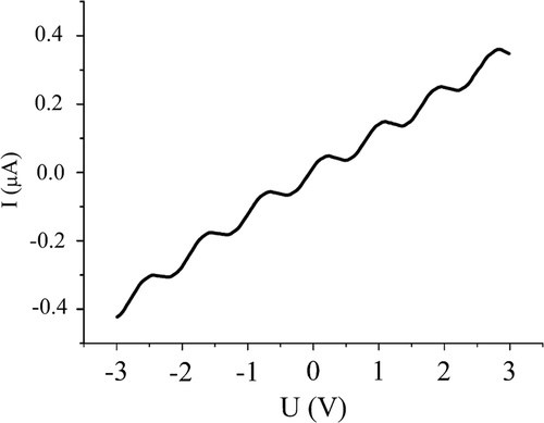
Actually, in our case, the inductive branch is well-visualised in low-frequency region (marked area upon the curve 2 in ). At such current flow mechanism, there may occur inner electric fields (electret polarisation which was actually expected to be formed by superimposition of permanent electric field at formation of the OS) which may cause delocalisation of carriers at superimposition of a nanostructure due to the trapping of the Fermi level by the hopping of delocalised states. Indeed, curve 3 in and support such a possibility. At the same time, illumination of this structure by light in the spectral region of the fundamental absorption can cause an increase of carrier concentration due to nonequilibrium carriers, and consequently the further decrease of ρ(ω) (curve 4 in ). The same effect is observed while using additional illumination, apart from the electric field, during the process of OS formation (measurements in the dark). The latter may be treated as the formation of photoelectret state at nano-level. Thus, we may represent the formed nanostructure GaSe <OS> as N-barrier structure in which we may observe a single-electron tunnelling at certain conditions. This is confirmed by a thin current–voltage structure () where we can clearly visualise the Coulomb steps with a step 0.32 V for a nanostructure formed at normal conditions. As it was expected, the illumination during the formation blurs the Coulomb steps.
Figure 5. Thin structure of current–voltage characteristics of the expanded GaSe matrix after the formation of molecular interlayers of OS at normal conditions.
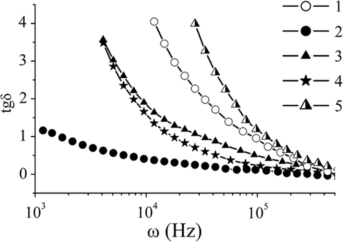
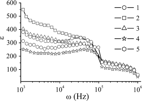
To shed light on the observed phenomena, we have measured frequency dependencies of dielectric permittivity ϵ(ω) along the crystallographic axis-c for the frequency region in which the dielectric loss tangent () is generally less than 1 (). It should be mentioned that not only the increase of ϵ(ω) but also its anomalous frequency dispersion (at ω > 1000 Hz the growth of ϵ(ω) at ω increasing) may be caused by the occurrence of additional polarisation at a hopping charge transfer Citation21. Thus, it may be assumed that the high-frequency oscillations in ϵ(ω) observed in reflect a mini-zone character of the bands of localised states formed by means of a modelling potential of nano-interlayers of the OS. Whether or not, an indisputable positive practical aspect for the technology of radiofrequency capacitors (namely, combination of high value of dielectric permittivity and low value of dielectric loss tangent in manganese range) is evident.
Figure 6. Frequency dependences of the dielectric loss tangent, perpendicular to the layers of the expanded matrix GaSe prior to – (1) and after the formation of molecular interlayers of OS at normal conditions – (2), as well as at superimposition of electric field – (3), at mutual illumination – (5), (4) – curve 3, measured at illumination.
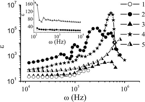
Figure 7. Frequency dependences of dielectric permittivity perpendicular to the layers of expanded GaSe matrix prior to – (1) and after the formation of molecular interlayers of OS at normal condition – (2), as well as at superimposition of electric field – (3), with the mutual illumination – (5), (4) – curve 3, measured at illumination. The inset shows a low-frequency region.
Dielectric permittivity has interesting behaviour at low frequency as shown in the inset of . One can see that ϵ(ω) increases essentially for a nanostructure formed in the electric field and simultaneous application of the light wave field. This signifies the formation of photoelectret polarisation Citation22.
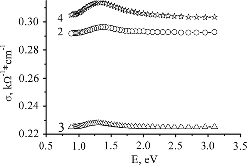
The introduction of OS into equidistantly extended semiconductor matrix with electron type of conductivity (InSe) also causes the increase of ρ(ω) but essentially smaller in magnitude (, curve 2), which was expected to happen accounting the similarity of the type of conductivity for both ingredients of nanostructure. However, contrary to p-GaSe, in this case the application of electric field at the formation of an OS in interlayer spacing of the matrix leads to a significant increase of specific resistance (, curve 3). Similarly to GaSe<OS>, additional illumination at the formation of nanostructure InSe<OS> decreases the mentioned growth. This decrease is enhanced if it is illuminated during measurements (, curve 5).
Figure 8. Frequency dependences of the real component of specific impedance perpendicular to the layers of expanded InSe matrix prior to – (1) and after the formation of molecular interlayers of OS at normal conditions – (2) as well as at superimposition of electric field – (3), at mutual illumination – (4). (5) – curve 4 measured at illumination.
shows the Nyquist diagram where the curves for both expanded matrix InSe (curve 1) and after introduction of molecules of OS into the matrix (curve 2) are practically parallel to the axis of the imaginary part of complex impedance. In general, the impedance model of such behaviour consists of a resistor and capacitor connected in series. This means that in case of violation of the conditions of resonance tunnelling, a capacitive blocking of a direct electron current along C is possible. However, the most interesting situation is observed at the formation of nanostructure in the electric field both with and without simultaneous illumination. In this case, high frequency horizontal branches appear in Nyquist diagrams (curves 3–5) whose nature is most probably linked with quantum capacitance () caused by both discretisation of electric spectrum of nanointerlayers InSe and by finite tunnelling time Citation23. This presume the following equivalent electric circuit (inset to ), where a sequential RC-link represents a classical barrier capacitance, while
represents the quantum one. Indeed, the computer parameter identification of this model yielded a good fit to the observed dependence.
Illumination of nanostructure InSe<OS> by visible light causes the generation of nonequilibrium carriers having energy sufficient for over barrier passage of the modified potential of van der Waals regions. As a result, their capacitance will be shunted by the conductivity of nonequilibrium carriers, and Nyquist diagram will transform to an arc-wise shape, which is precisely observed in the experiment (, curve 5).
Figure 9. Nyquist diagram constructed for an expanded InSe matrix along crystallographic axis-c prior to – (1) and after the formation of molecular interlayers of OS at normal conditions – (2), as well as at superimposition of electric field – (3), at mutual illumination – (4). (5) – curve 4 measured at illumination.
The above-proposed model also presumes a simultaneous change of screening impedance by a space charge of the available periodic barriers in the exterior electromagnetic field which may lead to Citation24 Maxwell–Wagner segmental polarisation. The latter causes the increase of a real component of permittivity which is observed in . Both, at the formation and at measurement, the illumination decrease the dielectric permittivity in a low-frequency region even in comparison with the initial expanded matrix, which is most probably related to a lower contribution of space charge component of polarisation due to a high value of electronic quasi-Fermi level.
Figure 10. Frequency dependences of dielectric permittivity perpendicular to the layers of expanded matrix InSe prior – (1) and after the formation of molecular interlayers of OS at normal condition – (2), as well as at superimposition of electric field – (3), at mutual superimposition of illumination – (4). (5) – curve 3 measured at illumination.
presents the dependences of photoresponse of InSe<OS> nanostructure in photoresistive mode. While the maximum decreases after the superimposition of electric field in the process of formation, the simultaneous illumination with the light wave field causes its increase. Herein, we observe the shift of the maximum into long-wave region by 0.1 eV for the first case (, curve 2) and by 0.03 eV for the second case (, curve 3). In this case, the long-wave shift
indicates the narrowing of the band gap due to an electron polarisation. Then, it is clear that illumination in the process of formation of the OS in the electric field causes an increase of the maximum
, and vice versa, leads to an observable decrease of the maximum of photo-electromotive force when measuring the photoresponse in photovoltaic mode.
Figure 11. Dependences of photoresponse of InSe<OS> nanostructure formed at normal conditions – (1), as well as at superimposition of electric field – (2), at mutual superimposition of illumination – (3).
4. Conclusions
Introduction of the OS (DiMe-PTCDI) into р-GaSe and n-InSe causes an increase of the specific resistance along the crystallographic axis-c as well as its frequency dispersion. A good visualisation of low-frequency inductive response in GaSe<OS> makes it possible to present the synthesised nanostructures as N-barrier structures, where a stepwise energy relief of quantum wells is caused by bending of energy levels at interphase boundaries. Most probably, the processes of capturing, holding and releasing the current carriers from quantum wells are responsible for an inductive response in GaSe<OS>. At the passage of direct electric current through GaSe<OS> perpendicular to nanointerlayers, a thin structure of current–voltage characteristic is in the shape of Coulomb steps with a step 0.32 V that are blurred due to simultaneous application of electric field and illumination. Applied electric field and simultaneous illumination during introduction of the OS in the expanded van der Waals regions of nonorganic semiconductor lead to the formation of electrets and photoelectret states that modify polarisation and photoprocesses in accordance with the conductivity type of nonorganic matrix. An essential contribution of quantum capacitance shows itself in InSe<OS> nanostructure formed in an electric field. The obtained nanostructure and techniques of their formation open a new approach to the technology of super high-capacitive radiofrequency capacitors as well as nanostructured elements of delay lines.
References
- Choy , JH , Kwon , SJ and Park , GS . 1998 . High-Tc superconductors in the two-dimensional limit: [(Py-CnH2n+1)2HgI4]-Bi2Sr2Cam−1CumOy (m = 1 and 2) . Science , 280 : 1589 – 1592 .
- Choy , JH , Kwak , SY , Park , JS , Jeong , YJ and Portier , J . 1999 . Intercalative nanohybrids of nucleoside monophosphates and DNA in layered metal hydroxide . J. Am. Chem. Soc. , 121 : 1399 – 1400 .
- Gusev , AI . 1998 . The effects of the nanocrystalline state in solids . Usp. Fiz. Nauk , 168 : 55 – 83 . (Physics-Uspekhi, in Russian)
- Grygorchak , II , Seredyuk , BO , Tovstyuk , KD and Bakhmatyuk , BP . 2002 . “ High-frequency capacitor nanostructure formation by intercalation ” . In New Trends in Intercalation Compounds for Energy Storage , Edited by: Julien , C , Pereira-Ramos , JP and Momchilov , A . 543 – 545 . Paris : Kluwer Academic Publisher .
- Voitovych , SA , Grygorchak , II and Aksimentyeva , OI . 2008 . Lateral semiconductive and polymer conductive nanolayered structures: Preparation, properties, and application . Mol. Cryst. Liq. Cryst. , 497 : 55 – 64 .
- Choy , JH , Paek , SM , Oh , JM and Jang , ES . 2002 . Intercalative route to heterostructured nanohybrids . Curr. Appl. Phys. , 2 : 489 – 495 .
- Ivashchyshyn , F . 2012 . I. Grygorchak, P. Stakhira, V. Cherpak, and M. Micov, Nonorganic semiconductor – Conductive polymer intercalate nanohybrids: Fabrication, properties, application, Curr. Appl. Phys. , 12 : 160 – 165 .
- Kuhn , A , Chevy , A and Chevalier , R . 1975 . Crystal structure and interatomic distance in GaSe . Phys. Status Sol. (b) , 31 : 469 – 473 .
- Chevy , A , Kuhn , A and Martin , M-S . 1977 . Large InSe monocrystals grown from a non-stoichiometric melt . J. Cryst. Growth. , 38 : 118 – 122 .
- Friend , RH and Yoffe , AD . 1987 . Electronic properties of intercalation complexes of the transition metal dichalcogenides . Adv. Phys. , 36 : 1 – 94 .
- Brütting , W . 2005 . Physics of Organic Semiconductors , Weinheim : Wiley .
- Stakhira , PY , Cherpak , VV and Yu. Volynyuk , D . 2009 . Properties of heterojunction based on pentacene and perylene derivatives . Semiconductors , 43 : 192 – 196 .
- Safran , SA . 1987 . “ Stage ordering in intercalation compounds ” . In Solid State Physics: Advances in Research and Applications , Edited by: Seitz , F , Turnbull , D and Ehrenreich , H . Vol. 40 , 183 – 246 . New York : Academic Press .
- Grigorchak , II , Netyaga , VV and Kovalyuk , ZD . 1997 . On some physical properties of InSe and GaSe semiconducting crystals intercalated by ferroelectrics . J. Phys.: Condens. Matter , 9 : L191 – L195 .
- Lee , YS . 2008 . Self Assembly and Nanotechnology , 344 Canada : John Wiley & Sons, Inc. Publication .
- Olekhnovich , NM , Moroz , II , Pushkarev , AV , Radyush , YuV , Salak , AN , Vyshatko , NP and Ferreira , VM . 2008 . Temperature impedance spectroscopy of (1 − x)Na1/2Bi1/2TiO3-xLaMg1/2Ti1/2O3 solid solutions . Phys. Solid State , 50 : 490 – 495 .
- Pollak , M and Geballe , TH . 1961 . Low frequency conductivity due to hopping processes in silicon . Phys. Rev. , 122 : 1742 – 1753 .
- Bisquert , J , Randriamahazaka , H and Garcia-Belmonte , G . 2005 . Inductive behaviour by charge-transfer and relaxation in solid-state electrochemistry . Electrochim. Acta , 51 : 627 – 640 .
- Penin , NA . 1996 . Negative capacitance in semiconductor structures . Semiconductors , 30 : 340 – 343 .
- Mora-Seró , I , Bisquert , J , Fabregat-Santiago , F and Garcia-Belmonte , G . 2006 . Implications of the negative capacitance observed at forward bias in nanocomposite and polycrystalline solar cells . Nano Lett. , 6 : 640 – 650 .
- Žukowski , PV , Partyka , J , Wegierek , P , Shostak , Yu , Sidorenko , Yu and Rodzik , A . 2000 . Dielectric properties of Cd1−xFexSe compounds . Semiconductors , 34 : 1124 – 1127 .
- Sesler , G . 1983 . Electrets , Moscow : Mir . (in Russian)
- Bonch-Bruevich , VL and Kalashnikov , SG . 1977 . Semiconductors Physics , Moscow : Nauka . (in Russian)
- Okutan , M , Basaran , E , Bakan , HI and Yakuphanoglu , F . 2005 . AC conductivity and dielectric properties of Co-doped TiO2 . Phys. B: Condens. Matter. , 364 : 300 – 305 .