
Abstract
This work describes the properties of gold nanoparticles (AuNPs) thin film on silicon (Si) substrates. The AuNPs can be divided into two major shapes: gold nanospheres (AuNSs) and gold nanorods (AuNRs). Two sizes of AuNSs (15 nm and 30 nm) and three aspect ratios of AuNRs (3.12, 3.39 and 3.60) were synthesised using the seeding-growth method. The AuNPs produced were deposited on Si substrates by using a spin-coating method followed by heat treatment at 200 °C. The number of AuNPs coatings varied as one, three and five coating depositions, respectively. From the field emission scanning electron microscopy, the AuNPs were uniformly distributed on the Si substrate surface. The AuNPs distribution increased with increasing number of AuNPs coating. Various deposited AuNPs with different shapes and sizes were analysed using current–voltage (I–V) measurement in light–dark conditions. The results showed that the resistance of samples became lower under light condition as the number of AuNPs coatings increased on the Si substrate due to the large amount of AuNPs particles, which had better properties in absorbing and scattering the light intensity. Among these samples, five-coating depositions of 15 nm AuNSs and 3.12 aspect ratio of AuNRs thin films gave the best sensitivity in light–dark condition. The higher sensitivity implied the better sensing and recovery properties since it can amplify a small signal from the same light source power/intensity.
1. Introduction
Gold nanoparticles (AuNPs) are a popular choice of nanomaterial for many researchers to work with because of their facile methods of synthesis, high degree of control over shape and size and long-term stability in a wide range of solvents and pH conditions.[Citation1] Moreover, AuNPs properties can be tuned by changing their size, which affect various properties such as light absorption, photoluminescence, magnetisation and electrical conductivity properties of the system that could benefit future nanodevices.[Citation1–3] The AuNPs thin film exhibits good memory effect and retention properties in electronic devices.[Citation4] Besides that, the AuNPs thin film plays a role in the sensing field.[Citation5] However, limited studies have been carried out on the effect of shape and size of AuNPs thin film on Si substrates without any ligand.
In this work, two sizes of gold nanospheres (AuNSs) and three aspect ratios of gold nanorods (AuNRs) were synthesised using the seeding-growth method. The produced AuNPs were spin coated on Si substrates. The nature of AuNPs thin film on Si substrates without any ligand was investigated. A field emission scanning electron microscope (FESEM) was used to observe the morphology of AuNPs thin film on Si. Using I–V measurements, the effect of size and shape of AuNPs on thin film properties was studied by varying the number of coatings.
2. Methodology
Two sizes of AuNSs (15 and 30 nm) and three aspect ratios of AuNRs (3.12, 3.39 and 3.60) were prepared using the seeding-growth method.[Citation1,Citation3,Citation6,7] The distribution of AuNPs diameters was determined by using transmission electron microscope (TEM, Philip CM 12) and approximately 100 nanoparticles were counted and measured for size distribution using the ImageJ software. For preparation of 15 nm AuNSs solution, HAuCl4 (125 mL, 254 μM) was heated to boiling temperature with continuous stirring at 350 rpm. Sodium citrate (2.5 mL, 40 mM) was rapidly added into the boiled solution and continuously stirred. The solution was boiled for another 10 minutes. The colour of the solution changed from faint blue to red wine throughout this process. The red wine colour solution was cooled down to room temperature by continuous stirring at 350 rpm for 15 minutes. Then, the solution was transferred into another beaker and left to cool to room temperature.
For the preparation of 30 nm AuNSs, an amount of 15 nm AuNSs was used as a seed solution. A 10 mL seed solution was added into 90 mL deionised water. The solution was stirred at 320 rpm for 2 minutes. Hydroxylamine hydrochloride, NH2OH.HCl (1 mL, 0.2 M) was added into the solution and continuously stirred for 5 minutes. Then, gold (III) chloride (0.5 mL, 25.4 mM) was added drop wise into the prepared solution. The stirring speed was set to 350 rpm and continuously stirred for another 5 minutes to complete the reaction. The colour of Au solution changed to dark red wine.
Three different aspect ratios of AuNRs (3.12, 3.39 and 3.60) were synthesised by using the seeding-growth method. To tune the aspect ratio of AuNRs, three different hexadecyltrimethylammonium bromide (CTAB) concentrations were used (0.1 M, 0.5 M and 1.0 M). The seeding-growth method of AuNRs was started by preparation of the seed solution. Firstly, the CTAB (5 mL) solution was mixed with HAuCl4 (5 mL, 0.0005 M). Then, ice-cold sodium borohydride (600 μL, 0.01 M) was added into the stirred solution for 2 minutes. Finally, a brownish yellow solution was formed. The sample was then kept at 25 °C.
Secondly, the growth solution was prepared by adding CTAB (5 mL) into AgNO3 solution (150 μL, 0.004 M). Then, HAuCl4 (5 mL, 0.001 M) and ascorbic acid (AA) (70 μL, 0.0788 M) were added into this solution. AA is a mild reducing agent that changed the growth solution from yellow to colourless. Finally, 50 mL of the seed solution was added into the growth solution. The solution colour gradually changed within 10–20 minutes. This solution was stored at 25 °C overnight without stirring. After that, the AuNRs solution was centrifuged at 14,000 rpm for 45 minutes and re-dispersed in deionised water. Centrifugation was repeated for three times in water in order to remove excess CTAB from the solution.
The prepared AuNPs was spin coated on Radio Corporation of America cleaned Si substrates at a spinning rate of 2000 rpm for 2 minutes (Laurell Technologies Corp.: WS-400B-6TFM/LITE/OND). A 20 μL AuNPs solution was used for each deposition with 10 minutes holding time. After the AuNPs thin film was deposited using the spin coater, the samples were placed in an oven to undergo heat treatment at 200 °C for 1 hour. The heat treatment process is important to ensure a good adhesion of the thin film on the Si substrates. Next, silver paste was screen printed on the samples and left to dry at room temperature.
In this work, the effect of AuNPs thin film with different shape and size on thin film properties was investigated. The number of spin coatings of AuNSs and AuNRs on Si substrates was varied in one coating, three coatings and five coatings. The morphology of the thin films was investigated by using FESEM. The degree of coverage was calculated based on the number of AuNPs per area of sample from SEM images. The electronic properties of the samples were investigated using current–voltage (I–V) measurement in the dark–light conditions. The I–V measurements were carried out using Optronics Lab OL 770-LED spectroradiometer and the voltage was swept from −2 V to 2 V.
3. Results and discussion
The TEM images of AuNPs were analysed by using ImageJ software to confirm the shape and size of AuNSs and AuNRs. The TEM images of AuNSs seeds (15 nm) and grown AuNSs (30 nm) are shown in Figure . The histograms of particle size distribution of the AuNSs are shown in Figure and the distribution was obtained based on 100 particles. From the results, it can be seen that the monodispersed spherical shapes of 15 nm and 30 nm AuNSs were obtained in the as synthesised solutions.
Figure 1. TEM images of AuNSs. (a) 15 nm and (b) 30 nm.
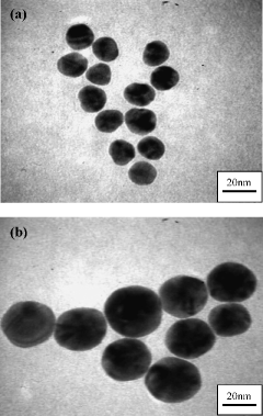
Figure 2. Histograms of distribution of particles size. (a) 15 nm AuNSs and (b) 30 nm AuNSs.
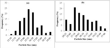
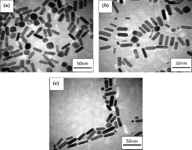
Figure shows the TEM images of AuNRs with various aspect ratios. The lengths and diameters of AuNRs were measured by using ImageJ software and summarised in Table . The increase of CTAB amount results in increasing the aspect ratio of AuNRs due to the preferential binding of surfactant CTAB on the {100} or the {110} faces, which leads to rods to be elongated along [110] direction.[Citation3]
Table 1. Average length, average diameter and aspect ratio of AuNRs measured from TEM images.
Figure 3. TEM micrographs of AuNRs. (a) 3.12 aspect ratio, (b) 3.39 aspect ratio and (c) 3.60 aspect ratio.
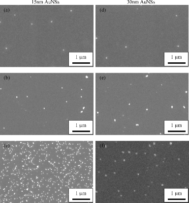
In this work, the AuNPs thin films were successfully deposited on Si substrates. The SEM micrographs in Figure show the 15 nm and 30 nm AuNSs thin film spin coated on the Si substrate with one coating, three coatings and five coatings, respectively. The degree of coverage on Si substrate with number of AuNSs coatings is shown in Table . The degree of coverage of AuNSs increased with increasing the number of coatings. Besides that, the size of the AuNSs affected the distribution on the Si substrate surface. By comparing the five coatings distribution of AuNSs in Figure (c) and (f), the 15 nm AuNSs thin film contained more particles compared to the 30 nm AuNSs thin film. The 15 nm AuNSs were finer than the 30 nm AuNSs particles. Hence, the same volume used during the spin-coating process caused a larger quantity of particles to be deposited on the substrate.
Table 2. Surface coverage density of various AuNSs coatings thin films.
Figure 4. SEM images. (a) 1 coating, (b) 3 coatings and (c) 5 coatings of 15 nm AuNSs, (d) 1 coating, (e) 3 coatings and (f) 5 coatings 30 nm AuNSs thin film on Si substrates.
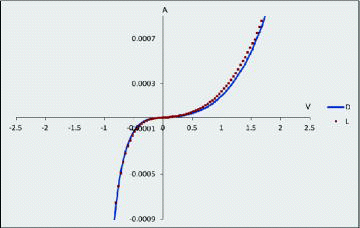
The schematic diagram of the structure of Si/AuNPs/Ag is shown in Figure . As a comparison, I–V analysis was carried out for the control sample (without AuNPs thin film layer) in the dark–light conditions as shown in Figure . The control sample shows Schottky curves with only a small change in the dark–light conditions (Figure ). The resistance of the control sample in visible light is 985.50 Ω and in dark is 1100.00 Ω with 0.10 sensitivity. The light source caused mobility of electrons to increase in the samples causing the samples to have low resistance.[Citation8] The schematic diagram in Figures and gave the idea on how electrons flow in the structure. Many applications of AuNPs are resulted from their magnificent interaction with light such as the optical–electronic properties.[Citation1] As the AuNPs have typical optical properties, they are sensitive to the changes of light–dark conditions.
Figure 5. Schematic diagram of structure Si/AuNPs/Ag.
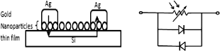
Figure 6. Schematic diagram of structure Si/Ag.
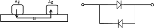
Figure 7. The current–voltage (I–V) curves of the control sample in light–dark conditions.
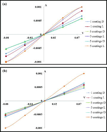
The prepared 15 nm and 30 nm AuNSs thin film samples (1 coating, 3 coatings and 5 coatings) were subjected to the I–V measurement in both light–dark conditions. The I–V curves show different resistance values. The resistance values were calculated using Ohm's law (V = I/R). The values were then used for calculation of the sensitivity between the light–dark conditions:
The ohmic curves were obtained with the AuNPs thin film embedded in the structure. Figure shows that the I–V curves were more steepened for the light condition compared to the dark condition of the samples. The light condition raised the current flow due to irradiation of light exciting a localised collective oscillation of free electrons on AuNPs. The change in oscillation frequency of the electrons for AuNPs then generated optical properties including absorption and scattering. Hence, the resistance was lower for the light condition compared to the dark condition. Besides that, in the light condition, increasing number of AuNPs thin film coatings leads to more steepened I–V curves as shown in Figure (a) and (b), due to the decreasing resistance of the samples. The number of AuNSs particles increased with increasing the coating deposition, that is in agreement with the SEM observation in Figure could cause more current flow due to the increasing mobility of electrons. In Figure (a), the curves for three coatings and five coatings in the dark condition for 15 nm AuNSs particle samples are overlapped. For 30 nm AuNSs samples in Figure (b), curves for three coatings in the light condition and five coatings in the dark condition are also overlapped. This observation is due to the too short measurement time for five coatings of 15 nm and 30 nm AuNSs samples in the dark condition. Measurements in the dark condition requires longer time than in the light condition in order to allow the system to relax.[Citation9]
Figure 8. The current–voltage (I–V) curves in light (L) and dark (D) conditions of various coatings of thin films on Si substrate: (a) 15 nm AuNSs solution and (b) 30 nm AuNSs solution.
The SEM micrographs of AuNRs thin film are shown in Figure . It can be seen that the uniform distribution of AuNRs was obtained on the Si substrate. The degree of coverage of AuNRs deposition on Si increased with increasing the thin film coatings number from 1, 3 and 5 coatings for 3.12, 3.39 and 3.60 aspect ratios AuNRs (Table ). This caused the density of AuNRs particles to become higher with increasing the coating number of AuNRs.
Table 3. Surface coverage density of various AuNRs coatings thin film.
Figure 9. SEM micrographs with various coatings of different aspect ratio AuNRs thin film on Si substrate. (a)–(c) 1, 3, 5 coatings of 3.12 aspect ratio AuNRs, (d)–(f) 1, 3, 5 coatings of 3.39 aspect ratio AuNRs and (g)–(i) 1, 3, 5 coatings of 3.60 aspect ratio AuNRs.
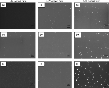
Figure shows the I–V curves of various coating number of different aspect ratios AuNRs thin film. It can be seen that the 3.12 aspect ratio AuNRs curve in the light condition is steeper compared to that in the dark condition, which shows the resistance of the sample in the light condition is lower. Similar results were observed for 3.39 and 3.60 aspect ratios AuNRs thin film. This low resistance occurs when more electrons flow as current in the samples. The light source caused mobility of electrons to increase in the samples and, as a result, the samples have low resistance.[Citation8] Besides that, the I–V curves became steeper with increasing coating number for 3.12, 3.39 and 3.60 aspect ratios AuNRs due to the presence of more particles deposited on the Si surface that could lower the resistance of the samples.
Figure 10. The current–voltage (I–V) curves in light (L) and dark (D) conditions of various coatings of different aspect ratios AuNRs thin films on Si substrates: (a) 3.12, (b) 3.39 and (c) 3.60 aspect ratios AuNRs.
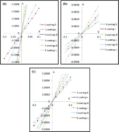
The values of sensitivity and resistance in the light–dark conditions of AuNPs thin film on Si substrate were calculated and tabulated in Table . By comparing the result through the size of AuNSs on Si substrate, it can be seen that the resistance of 15 nm AuNSs thin film was lower than 30 nm AuNSs thin film in the light–dark conditions. However, the sensitivity of light–dark value for 15 nm AuNSs thin film was higher than 30 nm AuNSs thin film due to the surface area of the particles. The surface area for 15 nm AuNSs was larger than that of 30 nm AuNSs. The optical absorption was enhanced due to the increase of surface area. The enhancement in optical absorption increased the conversion efficiency of light to electricity.[Citation10] For AuNRs thin film on Si, the resistance increased with increasing the aspect ratio from 3.12, 3.39 and 3.60. The result is in agreement with the SEM result in Figure as the AuNRs with 3.12 aspect ratio contain more AuNRs distribution on Si that leads to more current flow to lower the resistance. Hence, the curves in Figure (a) are steeper than those in Figure (b) and (c). Besides that, the sensitivity value of 3.12 aspect ratio AuNRs is higher than 3.39 and 3.60 aspect ratios (Table ). The result is in agreement with the degree of AuNRs coverage on Si substrate (Table ). The higher degree of AuNRs coverage leads to more current flow on the samples that lower the resistance.
Table 4. Resistance and sensitivity with varying coating layers of different size AuNSs and AuNRs thin film.
In this study, when the samples were exposed to visible light, the surface plasmon resonance of the nanoparticle thin films was enhanced. The conductance of the thin film increased when the surface plasmon in nanoparticle thin films was optically excited. The heat generation in AuNPs was strongly enhanced by the excitation of surface plasmon resonance. Similar result was observed by Govorov et al.[Citation11] The increase in heat generates mobile charge carriers, which in turn caused an increase in conductivity. Hence, the resistivity became lower when the AuNPs thin film is exposed to visible light.[Citation12]
For both AuNSs and AuNRs, the number of particles increased with increasing coating number. The larger number of AuNPs on Si substrate leads to more current flow in the samples because light irradiation excites a localised collective oscillation of free electrons on AuNPs. The change in oscillation frequency of the electrons for AuNPs then generated optical properties including absorption and scattering. Moreover, as the optical and thermal sensitivities were in fact closely related, AuNPs can be considered as nanometric heat sources and probes for local temperature variations via their optical behaviour.[Citation13] So, heat was generated when the samples were exposed to light irradiation. Then, the generated heat enhanced electron mobility and caused the increase of the current flow in the samples. Hence, the surface resistance of the samples decreased upon exposure to light irradiation.
The electrical properties of 15 nm AuNSs thin film are better than those of 30 nm AuNSs thin film because 15 nm AuNSs have larger surface area. Besides that, the 3.12 aspect ratio of AuNRs thin film exhibits better electrical properties than 3.39 and 3.60 aspect ratios of AuNR thin film. Uniform distribution of 3.12 aspect ratio AuNRs contributes to better sensitivity value compared to 3.39 and 3.60 aspect ratios AuNRs. Larger aspect ratio leads the AuNRs to lie flat or protrude like a needle on subsequent coating. However, excellent distribution of 5 coatings of 15 nm AuNSs thin film shows better electrical properties than 5-layer coating 3.12 aspect ratio AuNRs thin film, which is in agreement with the SEM observation (Figure ). The 5 coatings of 15 nm AuNSs thin film and better sensitivity of light–dark resistance in I–V measurements (Table ).
The sensitivity value in the light–dark condition also becomes higher as the coating deposition increases due to the presence of a large amount of AuNPs, which have better properties in absorbing and scattering the light. The higher sensitivity implies better sensing and recovery properties since it can amplify small signal from the same light source power/intensity. Hence, the effect of size and shape of AuNPs on Si electrical properties can be studied in sensor application for future work.
4. Conclusion
In this study, different sizes of AuNSs (15 nm and 30 nm) and various aspect ratios of AuNRs (3.12, 3.40 and 3.60) were successfully spin coated on one, three and five coating depositions on Si substrates. The SEM micrographs showed excellent distribution of AuNPs thin film on Si substrate. The 15 nm AuNSs and 3.12 aspect ratio AuNRs gave the highest sensitivity in the light–dark conditions.
Acknowledgements
The authors appreciate the technical support from School of Materials and Mineral Resources Engineering, Institute for Research in Molecular Medicine, School of Physics, Universiti Sains Malaysia. This research was funded by research university grant 1001/PSKBP/8630019, PGRS 1001/Pbahan/8630019). The first author received financial support from the Ministry of Higher Education under MyBrain Program.
References
- Jennings T, Strouse G. Past, present, and future of gold nanoparticles. Adv Exp Med Biol. 2007;620:34–47.
- Brown KR, Natan MJ. Hydroxylamine seeding of colloidal au nanoparticles in solution and on surfaces. Langmuir. 1998;14(4):726–728.
- Murphy Catherine J, Sau TK. Anisotropic metal nanoparticles: synthesis, assembly, and optical applications. Am Chem Soc. 2005;109(29):13857–13870.
- Leu C-C, Chen S-T, Liu F-K. Spin-coating-derived gold-nanoparticle memory. J Am Ceram Soc. 2010;93:3142–3147.
- Dominik E, Swen R, Alexander K, Annemarie P. Surface enhanced infrared absorption on Au nanoparticle films deposited on SiO2/Si for optical biosensing: detection of the antibody-antigen reaction. Surf Sci Lett. 2006;600(23):L305–L308.
- Daniel MC, Didier A. Gold nanoparticles: assembly, supramolecular chemistry, quantumsize-related properties, and applications toward biology, catalysis, and nanotechnology. Chem Rev. 2004;104:293–346.
- Nguyen NL, Le VV, Chu DK, Sai CN, Cao TN, Pham TH, Nguyen DT, Luu MQ. Synthesis and optical properties of colloidal gold nanoparticles. J Phys Conf Ser. 2009;187:012026.
- Reger, Daniel L, Goode, Scott L, Ball, David W. Chemistry: principles and practice, 3rd ed. Chemistry Department Books. Book 1; 2010.
- Raimondo C, Crivillers N, Reinders F, Sander F, Mayor M, Samorı P. Optically switchable organic field-effect transistors based on photoresponsive gold nanoparticles blended with poly(3-hexylthiophene). Proc Natl Acad Sci U.S.A. 2012;109(31):12375–12380.
- Zhao QZ, Ciobanu F. Enhancement of optical absorption and photocurrent of 6H-SiC by laser surface nanostructuring. Appl Phys Lett. 2007;91:121107.
- Govorov AO, Zhang W, Skeini T, Richardson H, Lee J, Kotov N. Gold nanoparticle ensembles as heaters and actuators: melting and collective plasmon resonances. Nanoscale Res Lett. 2006;1(1):84–90.
- Mangold MA, Weiss C. Surface plasmon enhanced photoconductance of gold nanoparticle arrays with incorporated alkane linkers. Appl Phys Lett. 2009;94:161104.
- Bruno P, Yannick G, Majid RH, Dominique P. Gold nanoparticles assemblies: thermal behaviour under optical excitation. Gold Bull. 2008;41(2):105–115.